These authors contributed equally \alsoaffiliationDepartment of Physics, An-Najah National University, Nablus, Palestine \altaffiliationThese authors contributed equally
Assessing carrier mobility, dopability, and defect tolerance in the chalcogenide perovskite BaZrS3
1 Abstract
The chalcogenide perovskite BaZrS3 has attracted much attention as a promising solar absorber for thin-film photovoltaics. Here, we use first-principles calculations to evaluate its carrier transport and defect properties. We find that BaZrS3 has a phonon-limited electron mobility of 37 cm2/Vs comparable to that in halide perovskites but lower hole mobility of 11 cm2/Vs. The defect computations indicate that BaZrS3 is intrinsically n-type due to shallow sulfur vacancies, but that strong compensation by sulfur vacancies will prevent attempts to make it p-type. We also establish that BaZrS3 is a defect-tolerant absorber with few low formation energy, deep intrinsic defects. Among the deep defects, sulfur interstitials are the strongest nonradiative recombination centers which in sulfur-rich conditions would limit the carrier lifetime to 10 ns. Our work highlights the material’s intrinsic limitations in carrier mobility and suggests suppressing the formation of sulfur interstitials to reach long carrier lifetime.
2 Introduction
Lead halide perovskites have revolutionized the field of photovoltaics (PV) by opening a promising path to earth-abundant, easily processable, and high-efficiency thin-film technologies.1, 2 The exceptional PV performance of halide perovskites is however shadowed by their poor stability.3 Structural analogy has motivated the search for alternative solar absorbers forming in the perovskite structure but in chemistries that could be more stable.4, 5, 6, 7, 8, 9, 10, 11, 12, 13 The chalcogenide perovskites ABX3 (A=Ca, Sr, Ba, B=Ti, Zr, and X=S, Se) have emerged in this context with their first suggestion as solar absorbers coming from first-principles studies4 followed by experimental synthesis and characterization especially of BaZrS3.14, 15, 16, 17, 18 BaZrS3 shows excellent stability in ambient conditions and exhibits a 1.8 eV direct band gap which can be tuned to 1.5 eV by alloying with BaTiS3 or BaZrSe3.14, 16, 17, 18, 19, 20, 21, 22, 23 Significant efforts have been dedicated to growing high-quality thin films of BaZrS3 and its alloys, using a range of techniques such as pulsed laser deposition,24, 25, 26 sputtering,20, 27, 28 molecular beam epitaxy,29, 30 and solution-based synthesis.31, 32, 33 Very recently, a proof-of-concept BaZrS3 solar cell has been reported, demonstrating an efficiency of 0.11%.34 Interestingly, BaZrS3 also stands out as a top candidate in a few high-throughput computational screening of thin-film solar absorbers.35, 36, 10, 37
In this letter, we use first-principles calculations to clarify the carrier transport and defect properties in BaZrS3. We compute the phonon-limited carrier mobility showing that BaZrS3 has intrinsically low hole mobility. We also perform state-of-the-art hybrid-functional defect calculations. We show that BaZrS3 is intrinsically n-type, and that p-type doping of BaZrS3 will be very difficult due to strong compensation by intrinsic donor defects. While BaZrS3 shows high defect tolerance with few low formation energy, deep defects, the sulfur interstitial (Si) is identified as the most worrisome nonradiative recombination center. Our results suggest pathways regarding growth condition optimization and device design towards high-performance BaZrS3 absorbers.
3 Results
3.1 Electronic band structure and carrier transport
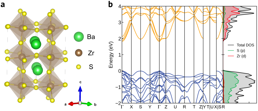
BaZrS3 forms in an orthorhombic Pnma perovskite structure (see Figure 1a). Our calculated band structure using the Heyd-Scuseria-Ernzerhof hybrid functional (HSE06)38 shows a direct band gap of 1.81 eV at the point (Figure 1b), in agreement with previous calculations and experiment.39, 4, 10, 16, 17, 18, 19, 20, 21, 22. Combining computed electronic and phonon properties, we find a phonon-limited carrier mobility of 11 cm2/Vs for holes and 37 cm2/Vs for electrons, with the carrier scattering mechanism dominated by polar optical phonons (see the supporting information for details). These values are upper bounds as realistic polycrystalline films will have additional scatterings from grain boundaries, impurities, and others. They are much lower than those calculated for conventional thin-film inorganic solar absorbers (such as CdTe40, 41 and Cu2ZnSnS442). The calculated hole mobility of BaZrS3 is also lower than for the halide perovskite CH3NH3PbI3 (11 vs 47 cm2/Vs), yet these two materials have comparable calculated electron mobility.43 Our results are consistent with experiments on BaZrS3 thin films which indicate low carrier mobilities (2 cm2/Vs for holes and 10–20 cm2/Vs for electrons).24, 44, 25, 45The measured low carrier mobility has been often attributed to small grain size or impurity scattering.24, 25 While these could be limiting factors in the experiments, our results highlight that BaZrS3 has intrinsically low phonon-limited carrier mobility, and that experimentally it is very unlikely to achieve mobilities higher than our computed values. We note that Ye et al. reported a very high sum mobility (100 cm2/Vs) in BaZrS3 films based on time-resolved photoluminescence (TRPL) measurements but the data suffer from reported very large uncertainty.46
The large difference between hole and electron mobilities directly comes from the electronic band structure (see Figure 1b). The lower conduction bands are much more dispersive than the upper valence bands. As a result, the effective mass is found to be small for electrons (0.3 ) and relatively large for holes (0.9 ). The fundamental difference in hole effective mass and mobility between BaZrS3 and CH3NH3PbI3 comes from the different electronic character in the valence band. While the halide perovskite mixes anion and cation orbitals leading to delocalized valence band,47 the sulfide shows a more ionic behavior with the valence band being mainly of anion character (see Figure 1b).
3.2 Intrinsic point defects and doping
We have calculated all the intrinsic point defects in BaZrS3 including the vacancies (, , ), interstitials (Bai, Zri, Si), and antisites (BaZr, ZrBa, BaS, SBa, ZrS, SZr). Our first-principles calculations are all performed using the HSE06 hybrid functional and large supercell (360 atoms) with proper charge correction and spin-polarization, which is different from previous first-principles calculations.16, 48 We provide in the supporting information the details of our methodology and a comparison to previous calculations. We note that some of the defects (e.g., Si) involve several configurations that are close in energy. In the following, we report only results for the lowest energy configurations, while those for metastable configurations can be found in Figure S2 of the supporting information.
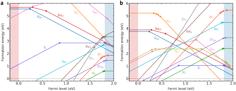
Figures 2 shows the formation energies of the intrinsic defects in BaZrS3 for both S-poor and S-rich conditions. The defect charge-state transition levels are plotted in Figure 3. We find that a series of shallow donor defects can form in BaZrS3. The is the dominant donor, giving rise to two donor levels (/0) and (2/) that are almost in resonance with the conduction band. Under S-poor conditions (Figure 2a), the has fairly low formation energy and thus exists in high concentration. On the other hand, the acceptor defects, mainly and BaZr, have high formation energies. These indicate that S-poor BaZrS3 will be heavily n-type doped by the donors. Under S-rich conditions (Figure 2b), the formation energy of is increased, while the formation energies of the acceptor defects are reduced. Under those conditions, the equilibrium Fermi level would be pinned close to the intersection of the formation energies of and (about 0.5 eV below the conduction band), indicative of a very weak n-type, almost intrinsic BaZrS3. Our results explain the experimental observation that as-grown BaZrS3 is intrinsically n-type with the electron concentration as high as 1019–1020 cm-3,24 and we attribute this doping to sulfur vacancies.
Figure 2 also indicates that it will be very difficult to achieve p-type BaZrS3. While , , and BaZr are shallow acceptors, they are strongly compensated by the donors. Even under the most favorable S-rich conditions, Fermi-level pinning energy for p-type doping49, 50 is 0.6 eV above the VBM, caused by the whose formation energy drops first to zero when the Fermi level is approaching the VBM (Figure 2b). In view of the high p-type pinning limit, any extrinsic shallow acceptors will be strongly compensated, thus preventing p-type doping. In the literature, p-type BaZrS3 has only been reported once with hole concentration of 10.27 We note that this was achieved in a sample which is extremely Ba-deficient (Ba/Zr ratio as low as 0.6), raising questions about possible secondary phases.
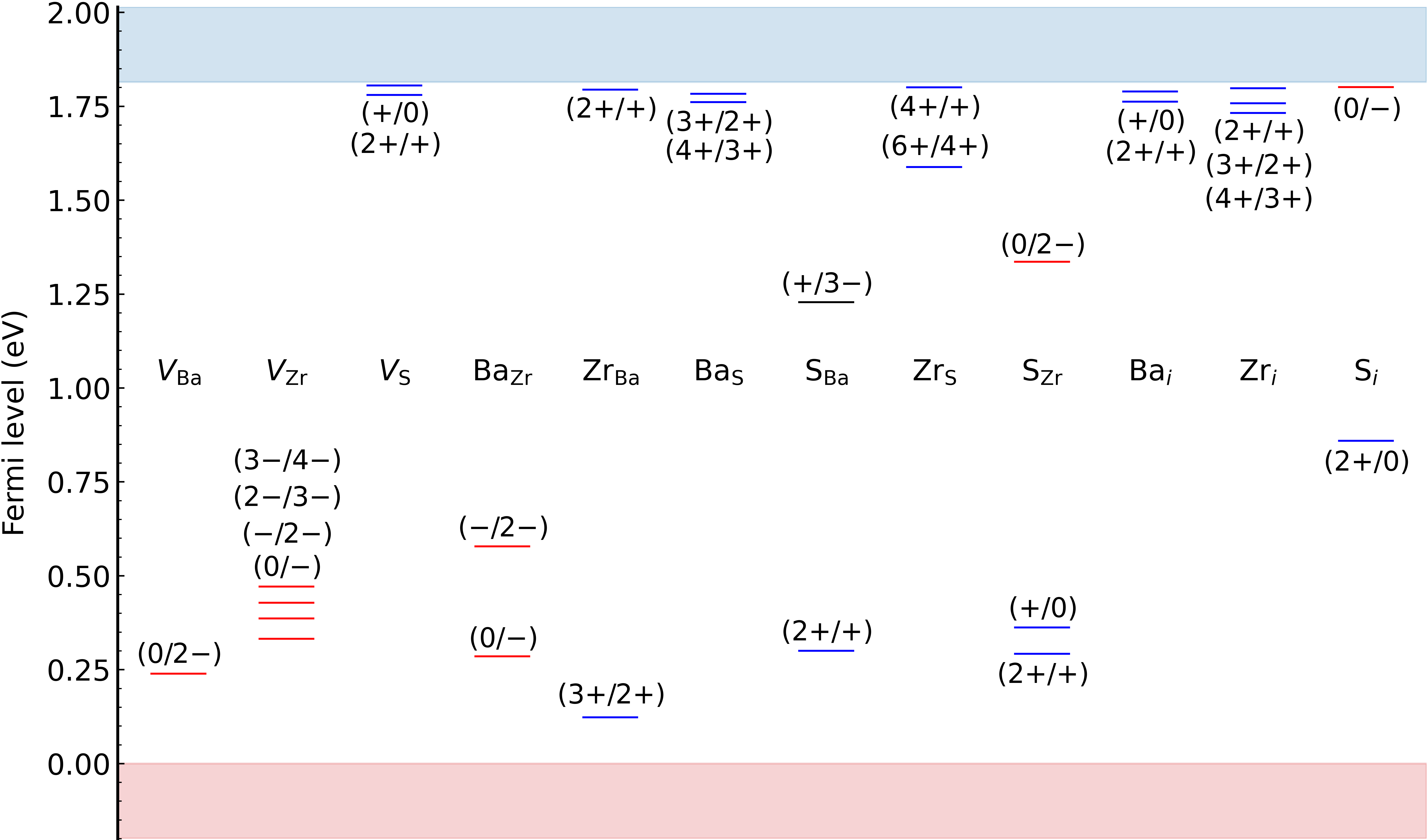
Next to doping, from Figures 2 and 3 we identify a few defects with deep transition levels, including (3/4), BaZr (/2), SBa (/3), SZr (0/2), and Si (0/2). Only Si has sufficiently low formation energy to exist in significant concentration (when in S-rich conditions; see Table S4 for the calculated defect concentrations). Since defect-assisted nonradiative recombination is one of the key processes that limit carrier lifetime and ultimately solar cell performance,51, 52, 53, 54, 55, 56, 57 it is necessary to assess whether the Si is an efficient nonradiative recombination center.
3.3 Nonradiative carrier capture by sulfur interstitials
We now compute the nonradiative capture coefficients of the Si. For nonradiative capture by the Si, the relevant charge-state transitions are (2/) and (/0), which are located at 0.35 and 1.37 eV above the VBM, respectively, as shown in Figure 4a. There are two capture processes associated with the (/0) level: for hole () capture and for electron () capture, where the superscript denotes the initial charge state.58, 59 Similarly, nonradiative recombination via the (2/) level involves two capture processes: and .
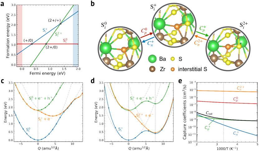
To illustrate the capture processes, Figure 4b shows the local atomic structures of the Si in the three charge states: 0, , and 2. The local structures of S and S are similar but differ from that of S. In the 0 and charge states, the interstitial S forms distorted tetrahedral bonds with two Ba, one Zr, and one S nearest neighbors. With the S S transition (i.e., capturing a hole, ), another lattice S atom moves towards the interstitial S. This lattice S atom and the interstitial S move further closer with the S S transition (i.e., capturing another hole, ). As a result, the S forms a S trimer.
The configuration coordinate diagrams (CCDs) for the Si (/0) and (/) transitions are shown in Figures 4c and 4d. Such diagrams map the potential energy surfaces (PESs) of a defect in two adjacent charge states for a given transition as a function of a generalized configuration coordinate (Q).60, 61, 62 We find that the Q displacement is larger for the (/) transition than for the (/0) transition, reflecting the structural differences discussed above. The CCDs indicate anharmonic atomic vibrations in the Si capture processes, which are pronounced for those associated with the (/) transition; see a comparison between the anharmonic and harmonic PESs in Figures 4c, 4d and S3. Anharmonicity in the CCDs was widely found for nonradiative carrier capture in halide perovskites and other low-symmetry semiconductors.63, 64, 59, 65, 66 The anharmonicity reduces the electron capture barrier of S but increases the electron capture barrier of S, compared to capture barriers in the harmonic approximation. Both S and S have a negligibly small hole capture barrier. From the capture barriers, the Si is expected to be an efficient nonradiative recombination center.
Figure 4e shows the calculated four capture coefficients versus temperature. The results suggest fast electron capture by S with of at room temperature and slow electron capture by S with of . The hole capture by S is fast with a room-temperature of , while it is slow for S with of . The latter is due to relatively small vibrational overlap between the PESs for the S S transition. In low-doped or intrinsic BaZrS3, by balancing electron and hole capture under steady-state conditions, the total capture coefficient () is given by58, 66
At room temperature, the is calculated to be . This is a moderate value, limited by the relatively slow hole and electron capture by S. It is slightly smaller than the value () for the dominant recombination centers (iodine interstitials, Ii) in computed in a similar theoretical framework.63, 59
3.4 Discussion
BaZrS3 shows higher electron mobility than hole mobility which would suggest using this material as a p-type absorber layer as it is the diffusion length of minority carriers that mainly controls the solar cell efficiency.67, 68 Our analysis however shows that it will be unlikely to make p-type BaZrS3. Using the intrinsically n-type doped BaZrS3 as an absorber layer will lead to smaller minority-carrier diffusion lengths limited by the lower hole mobility and also cause issues at the device level as discussed for other n-type absorbers 69, 70. We thus suggest it could be more viable to devise a p-i-n (or n-i-p) cell using BaZrS3 as the intrinsic layer (lightly n-type doped), as in halide perovskite solar cells.71 In such a p-i-n device, the carrier diffusion length is controlled by the ambipolar mobility () which is estimated to be 17 cm2/Vs using our calculated intrinsic electron and hole mobilities.72, 73, 74 Preparing intrinsic BaZrS3 requires to reduce dramatically the concentration of donors which can be achieved using S-rich growth conditions. However, S-rich conditions would enhance the formation of the nonradiative recombination centers, the Si. It might then be beneficial to reduce electron concentration by introducing an extrinsic shallow acceptor while keeping a low sulfur chemical potential.
We estimate now a realistic upper bound of the Si density in high-temperature synthesized BaZrS3 samples. Under S-rich conditions and assuming 1000 K growth of BaZrS3 and rapid quenching to room temperature, the Si density is estimated to be on the order of (see Table S4). This high Si density leads to a nonradiative recombination coefficient () on the order of at room temperature; here is defined as , where is the defect density.75, 76, 59 As a result, the nonradiative lifetime () is on the order of 10 ns for S-rich conditions. Moving to less S-rich conditions will reduce the Si density and increase the carrier lifetime. Our results are in reasonable quantitative agreement with the carrier lifetime on the order of 50 ns measured by TRPL on BaZrS3 single-crystal samples.46 In comparison, the Ii in has been found to lead to a much longer nonradiative lifetime, on the order of 100 ns,63, 59 based on the fact that the deep-level trap density in solution-processed samples is on the order of .77, 78, 79
Ye et al. estimated the solar cell figure of merit () of BaZrS3 based on experimental data and using , where is the optical absorption coefficient and the carrier diffusion length.46, 80, 72, 81, 82 They found a value of 2.1 using an absorption coefficient of 4940 cm-1, nonradiative lifetime of 50 ns, and mobility of 146.2 cm2/Vs.46 Our computational results do not disagree with the lifetime but raise strong doubts on the mobility value. Since our calculated mobility is an order of magnitude lower, we estimate the to be 0.33. Our results however indicate that if the Si concentration is lowered or the interstitials are passivated in some way, higher carrier lifetime could be reached which will boost the figure of merit.
In addition to intrinsic defects, we briefly mention that BaZrS3 is tolerant to oxygen impurities which could be present in high concentration in the samples prepared by sulfurization of BaZrO3 precursor.24, 83 We find that the oxygen-related point defects, including oxygen interstitial (Oi) and O substitution on the S site (OS), are electrically inactive, i.e., they are stable in the neutral charge state for almost the entire range of Fermi levels (see Figure S4 of the supporting information), in agreement with previous experimental and theoretical studies.83
4 Conclusions
We evaluated carrier transport and defect properties in the chalcogenide perovskite solar absorber BaZrS3. Our results show that BaZrS3 has a lower hole mobility than electron mobility (11 vs 37 cm2/Vs). The mobility in this sulfide perovskite is lower and more asymmetric (in terms of hole versus electron mobilities) than in lead halide perovskites. Our defect computations indicate an intrinsic tendency for n-type doping due to the shallow donor and that p-type doping is very unlikely to be achievable. We confirm that overall BaZrS3 is a defect-tolerant absorber with few deep defects that could act as nonradiative recombination centers. The Si is identified to be the most problematic deep center. Under S-rich conditions, the carrier capture by the Si will lead to a carrier lifetime on the order of 10 ns. Our work strongly suggests that suppressing the formation of Si is critical for BaZrS3 to be a high-performance absorber.
5 Supporting Information Available
Full description of the computational methods. Supplementary Tables S1–S5, Figures S1–S4, and Refs. S1–S29.
6 Notes
The authors declare no competing financial interest.
7 Acknowledgments
This work was supported by the U.S. Department of Energy, Office of Science, Basic Energy Sciences under award number DE-SC0023509. This research used resources of the National Energy Research Scientific Computing Center (NERSC), a DOE Office of Science User Facility supported by the Office of Science of the U.S. Department of Energy under contract no. DE-AC02-05CH11231 using NERSC award BES-ERCAP0023830. A.P. acknowledges support from a Department of Education GAANN fellowship.
References
- Kojima et al. 2009 Kojima, A.; Teshima, K.; Shirai, Y.; Miyasaka, T. Organometal halide perovskites as visible-light sensitizers for photovoltaic cells. Journal of the American Chemical Society 2009, 131, 6050–6051
- 2 Best Research-Cell Efficiency Chart. https://www.nrel.gov/pv/cell-efficiency.html, U.S. National Renewable Energy Laboratory
- Correa-Baena et al. 2017 Correa-Baena, J.-P.; Saliba, M.; Buonassisi, T.; Grätzel, M.; Abate, A.; Tress, W.; Hagfeldt, A. Promises and challenges of perovskite solar cells. Science 2017, 358, 739–744
- Sun et al. 2015 Sun, Y.-Y.; Agiorgousis, M. L.; Zhang, P.; Zhang, S. Chalcogenide perovskites for photovoltaics. Nano Letters 2015, 15, 581–585
- Körbel et al. 2016 Körbel, S.; Marques, M. A.; Botti, S. Stability and electronic properties of new inorganic perovskites from high-throughput ab initio calculations. Journal of Materials Chemistry C 2016, 4, 3157–3167
- Zhao et al. 2017 Zhao, X.-G.; Yang, J.-H.; Fu, Y.; Yang, D.; Xu, Q.; Yu, L.; Wei, S.-H.; Zhang, L. Design of lead-free inorganic halide perovskites for solar cells via cation-transmutation. Journal of the American Chemical Society 2017, 139, 2630–2638
- Kuhar et al. 2017 Kuhar, K.; Crovetto, A.; Pandey, M.; Thygesen, K. S.; Seger, B.; Vesborg, P. C.; Hansen, O.; Chorkendorff, I.; Jacobsen, K. W. Sulfide perovskites for solar energy conversion applications: computational screening and synthesis of the selected compound LaYS3. Energy & Environmental Science 2017, 10, 2579–2593
- Chakraborty et al. 2017 Chakraborty, S.; Xie, W.; Mathews, N.; Sherburne, M.; Ahuja, R.; Asta, M.; Mhaisalkar, S. G. Rational design: A high-throughput computational screening and experimental validation methodology for lead-free and emergent hybrid perovskites. ACS Energy Letters 2017, 2, 837–845
- Lu et al. 2018 Lu, S.; Zhou, Q.; Ouyang, Y.; Guo, Y.; Li, Q.; Wang, J. Accelerated discovery of stable lead-free hybrid organic-inorganic perovskites via machine learning. Nature Communications 2018, 9, 3405
- Huo et al. 2018 Huo, Z.; Wei, S.-H.; Yin, W.-J. High-throughput screening of chalcogenide single perovskites by first-principles calculations for photovoltaics. Journal of Physics D: Applied Physics 2018, 51, 474003
- Cai et al. 2019 Cai, Y.; Xie, W.; Teng, Y. T.; Harikesh, P. C.; Ghosh, B.; Huck, P.; Persson, K. A.; Mathews, N.; Mhaisalkar, S. G.; Sherburne, M., et al. High-throughput computational study of halide double perovskite inorganic compounds. Chemistry of Materials 2019, 31, 5392–5401
- Gebhardt et al. 2023 Gebhardt, J.; Gassmann, A.; Wei, W.; Weidenkaff, A.; Elsässer, C. Screening for sustainable and lead-free perovskite halide absorbers–A database collecting insight from electronic-structure calculations. Materials & Design 2023, 234, 112324
- Wu and Ganose 2023 Wu, R.; Ganose, A. M. Tilt-induced charge localisation in phosphide antiperovskite photovoltaics. Journal of Physics: Materials 2023, 7, 015009
- Sopiha et al. 2022 Sopiha, K. V.; Comparotto, C.; Márquez, J. A.; Scragg, J. J. Chalcogenide perovskites: tantalizing prospects, challenging materials. Advanced Optical Materials 2022, 10, 2101704
- Choi et al. 2022 Choi, J. W.; Shin, B.; Gorai, P.; Hoye, R. L. Z.; Palgrave, R. Emerging Earth-Abundant Solar Absorbers. ACS Energy Letters 2022, 7, 1553–1557
- Meng et al. 2016 Meng, W.; Saparov, B.; Hong, F.; Wang, J.; Mitzi, D. B.; Yan, Y. Alloying and defect control within chalcogenide perovskites for optimized photovoltaic application. Chemistry of Materials 2016, 28, 821–829
- Perera et al. 2016 Perera, S.; Hui, H.; Zhao, C.; Xue, H.; Sun, F.; Deng, C.; Gross, N.; Milleville, C.; Xu, X.; Watson, D. F., et al. Chalcogenide perovskites–an emerging class of ionic semiconductors. Nano Energy 2016, 22, 129–135
- Niu et al. 2017 Niu, S.; Huyan, H.; Liu, Y.; Yeung, M.; Ye, K.; Blankemeier, L.; Orvis, T.; Sarkar, D.; Singh, D. J.; Kapadia, R., et al. Bandgap control via structural and chemical tuning of transition metal perovskite chalcogenides. Advanced Materials 2017, 29, 1604733
- Wei et al. 2020 Wei, X.; Hui, H.; Perera, S.; Sheng, A.; Watson, D. F.; Sun, Y.-Y.; Jia, Q.; Zhang, S.; Zeng, H. Ti-alloying of BaZrS3 chalcogenide perovskite for photovoltaics. ACS Omega 2020, 5, 18579–18583
- Comparotto et al. 2020 Comparotto, C.; Davydova, A.; Ericson, T.; Riekehr, L.; Moro, M. V.; Kubart, T.; Scragg, J. Chalcogenide perovskite BaZrS3: thin film growth by sputtering and rapid thermal processing. ACS Applied Energy Materials 2020, 3, 2762–2770
- Sadeghi et al. 2023 Sadeghi, I.; Van Sambeek, J.; Simonian, T.; Xu, M.; Ye, K.; Cai, T.; Nicolosi, V.; LeBeau, J. M.; Jaramillo, R. Expanding the Perovskite Periodic Table to Include Chalcogenide Alloys with Tunable Band Gap Spanning 1.5–1.9 eV. Advanced Functional Materials 2023, 33, 2304575
- Ye et al. 2024 Ye, K.; Sadeghi, I.; Xu, M.; Van Sambeek, J.; Cai, T.; Dong, J.; Kothari, R.; LeBeau, J. M.; Jaramillo, R. A Processing Route to Chalcogenide Perovskites Alloys with Tunable Band Gap via Anion Exchange. arXiv preprint 2024, https://doi.org/10.48550/arXiv.2403.09016
- Kayastha et al. 2024 Kayastha, P.; Longo, G.; Whalley, L. D. A First-Principles Thermodynamic Model for the Ba–Zr–S System in Equilibrium with Sulfur Vapor. ACS Applied Energy Materials 2024, https://doi.org/10.1021/acsaem.3c03208
- Wei et al. 2020 Wei, X.; Hui, H.; Zhao, C.; Deng, C.; Han, M.; Yu, Z.; Sheng, A.; Roy, P.; Chen, A.; Lin, J., et al. Realization of BaZrS3 chalcogenide perovskite thin films for optoelectronics. Nano Energy 2020, 68, 104317
- Yu et al. 2021 Yu, Z.; Wei, X.; Zheng, Y.; Hui, H.; Bian, M.; Dhole, S.; Seo, J.-H.; Sun, Y.-Y.; Jia, Q.; Zhang, S.; Yang, S.; Zeng, H. Chalcogenide perovskite BaZrS3 thin-film electronic and optoelectronic devices by low temperature processing. Nano Energy 2021, 85, 105959
- Ramanandan et al. 2023 Ramanandan, S. P.; Giunto, A.; Stutz, E. Z.; Reynier, B.; Lefevre, I. T. F. M.; Rusu, M.; Schorr, S.; Unold, T.; Morral, A. F. I.; Márquez, J. A., et al. Understanding the growth mechanism of BaZrS3 chalcogenide perovskite thin films from sulfurized oxide precursors. Journal of Physics: Energy 2023, 5, 014013
- Han et al. 2023 Han, Y.; Xu, J.; Liang, Y.; Chen, X.; Jia, M.; Zhang, J.; Lian, L.; Liu, Y.; Li, X.; Shi, Z. P-type conductive BaZrS3 thin film and its band gap tunning via Ruddlesden-Popper Ba3Zr2S7 and titanium alloying. Chemical Engineering Journal 2023, 473, 145351
- Jamshaid et al. 2024 Jamshaid, S.; Cicconi, M. R.; Heiss, W.; Webber, K. G.; Wellmann, P. J. Synthesis and Characterization of BaZrS3 Thin Films via Stacked Layer Methodology: A Comparative Study of BaZrS3 on Zirconium Foil and Silicon Carbide Substrates. Advanced Engineering Materials 2024, https://doi.org/10.1002/adem.202302161
- Sadeghi et al. 2021 Sadeghi, I.; Ye, K.; Xu, M.; Li, Y.; LeBeau, J. M.; Jaramillo, R. Making BaZrS3 chalcogenide perovskite thin films by molecular beam epitaxy. Advanced Functional Materials 2021, 31, 2105563
- Surendran et al. 2021 Surendran, M.; Chen, H.; Zhao, B.; Thind, A. S.; Singh, S.; Orvis, T.; Zhao, H.; Han, J.-K.; Htoon, H.; Kawasaki, M., et al. Epitaxial thin films of a chalcogenide perovskite. Chemistry of Materials 2021, 33, 7457–7464
- Ravi et al. 2021 Ravi, V. K.; Yu, S. H.; Rajput, P. K.; Nayak, C.; Bhattacharyya, D.; Chung, D. S.; Nag, A. Colloidal BaZrS3 chalcogenide perovskite nanocrystals for thin film device fabrication. Nanoscale 2021, 13, 1616–1623
- Turnley et al. 2022 Turnley, J. W.; Vincent, K. C.; Pradhan, A. A.; Panicker, I.; Swope, R.; Uible, M. C.; Bart, S. C.; Agrawal, R. Solution deposition for chalcogenide perovskites: a low-temperature route to BaMS3 materials (M= Ti, Zr, Hf). Journal of the American Chemical Society 2022, 144, 18234–18239
- Pradhan et al. 2023 Pradhan, A. A.; Uible, M. C.; Agarwal, S.; Turnley, J. W.; Khandelwal, S.; Peterson, J. M.; Blach, D. D.; Swope, R. N.; Huang, L.; Bart, S. C., et al. Synthesis of BaZrS3 and BaHfS3 chalcogenide perovskite films using single-phase molecular precursors at moderate temperatures. Angewandte Chemie International Edition 2023, 62, e202301049
- Dallas et al. 2024 Dallas, P.; Gkini, K.; Kaltzoglou, A.; Givalou, L.; Konstantakou, M.; Orfanoudakis, S.; Boukos, N.; Sakellis, E.; Tsipas, P.; Kalafatis, A., et al. Exploring the potential of powder-to-film processing for proof-of-concept BaZrS3 perovskite solar cells. Materials Today Communications 2024, 39, 108608
- Yuan et al. 2024 Yuan, Z. et al. Discovery of the Zintl-phosphide BaCd2P2 as a long carrier lifetime and stable solar absorber. Joule 2024, https://doi.org/10.1016/j.joule.2024.02.017
- Kuhar et al. 2018 Kuhar, K.; Pandey, M.; Thygesen, K. S.; Jacobsen, K. W. High-throughput computational assessment of previously synthesized semiconductors for photovoltaic and photoelectrochemical devices. ACS Energy Letters 2018, 3, 436–446
- Fabini et al. 2019 Fabini, D. H.; Koerner, M.; Seshadri, R. Candidate inorganic photovoltaic materials from electronic structure-based optical absorption and charge transport proxies. Chemistry of Materials 2019, 31, 1561–1574
- Heyd et al. 2003 Heyd, J.; Scuseria, G. E.; Ernzerhof, M. Hybrid functionals based on a screened Coulomb potential. The Journal of Chemical Physics 2003, 118, 8207–8215
- Polfus et al. 2015 Polfus, J. M.; Norby, T.; Bredesen, R. Protons in Oxysulfides, Oxysulfates, and Sulfides: A First-Principles Study of La2O2S, La2O2SO4, SrZrS3, and BaZrS3. The Journal of Physical Chemistry C 2015, 119, 23875–23882
- Ganose et al. 2021 Ganose, A. M.; Park, J.; Faghaninia, A.; Woods-Robinson, R.; Persson, K. A.; Jain, A. Efficient calculation of carrier scattering rates from first principles. Nature communications 2021, 12, 2222
- Vukmirović 2021 Vukmirović, N. Calculations of electron mobility in II-VI semiconductors. Phys. Rev. B 2021, 104, 085203
- Monserrat et al. 2018 Monserrat, B.; Park, J.-S.; Kim, S.; Walsh, A. Role of electron-phonon coupling and thermal expansion on band gaps, carrier mobility, and interfacial offsets in kesterite thin-film solar cells. Applied Physics Letters 2018, 112, 193903
- Poncé et al. 2019 Poncé, S.; Schlipf, M.; Giustino, F. Origin of low carrier mobilities in halide perovskites. ACS Energy Letters 2019, 4, 456–463
- Márquez et al. 2021 Márquez, J. A.; Rusu, M.; Hempel, H.; Ahmet, I. Y.; Kölbach, M.; Simsek, I.; Choubrac, L.; Gurieva, G.; Gunder, R.; Schorr, S.; Unold, T. BaZrS3 Chalcogenide Perovskite Thin Films by H2S Sulfurization of Oxide Precursors. The Journal of Physical Chemistry Letters 2021, 12, 2148–2153
- Ravi et al. 2021 Ravi, V. K.; Yu, S. H.; Rajput, P. K.; Nayak, C.; Bhattacharyya, D.; Chung, D. S.; Nag, A. Colloidal BaZrS3 chalcogenide perovskite nanocrystals for thin film device fabrication. Nanoscale 2021, 13, 1616–1623
- Ye et al. 2022 Ye, K.; Zhao, B.; Diroll, B. T.; Ravichandran, J.; Jaramillo, R. Time-resolved photoluminescence studies of perovskite chalcogenides. Faraday Discussions 2022, 239, 146–159
- Yin et al. 2015 Yin, W.-J.; Yang, J.-H.; Kang, J.; Yan, Y.; Wei, S.-H. Halide perovskite materials for solar cells: a theoretical review. Journal of Materials Chemistry A 2015, 3, 8926–8942
- Wu et al. 2021 Wu, X.; Gao, W.; Chai, J.; Ming, C.; Chen, M.; Zeng, H.; Zhang, P.; Zhang, S.; Sun, Y.-Y. Defect tolerance in chalcogenide perovskite photovoltaic material BaZrS3. Science China Materials 2021, 64, 2976–2986
- Robertson and Clark 2011 Robertson, J.; Clark, S. Limits to doping in oxides. Physical Review B 2011, 83, 075205
- Walsh and Zunger 2017 Walsh, A.; Zunger, A. Instilling defect tolerance in new compounds. Nature Materials 2017, 16, 964–967
- Repins et al. 2013 Repins, I.; Moutinho, H.; Choi, S.; Kanevce, A.; Kuciauskas, D.; Dippo, P.; Beall, C.; Carapella, J.; DeHart, C.; Huang, B., et al. Indications of short minority-carrier lifetime in kesterite solar cells. Journal of Applied Physics 2013, 114, 084507
- Brandt et al. 2015 Brandt, R. E.; Stevanović, V.; Ginley, D. S.; Buonassisi, T. Identifying defect-tolerant semiconductors with high minority-carrier lifetimes: beyond hybrid lead halide perovskites. MRS Communications 2015, 5, 265–275
- Jaramillo et al. 2016 Jaramillo, R.; Sher, M.-J.; Ofori-Okai, B. K.; Steinmann, V.; Yang, C.; Hartman, K.; Nelson, K. A.; Lindenberg, A. M.; Gordon, R. G.; Buonassisi, T. Transient terahertz photoconductivity measurements of minority-carrier lifetime in tin sulfide thin films: Advanced metrology for an early stage photovoltaic material. Journal of Applied Physics 2016, 119, 035101
- Park et al. 2018 Park, J. S.; Kim, S.; Xie, Z.; Walsh, A. Point defect engineering in thin-film solar cells. Nature Reviews Materials 2018, 3, 194–210
- Guillemoles et al. 2019 Guillemoles, J.-F.; Kirchartz, T.; Cahen, D.; Rau, U. Guide for the perplexed to the Shockley–Queisser model for solar cells. Nature Photonics 2019, 13, 501–505
- Kim et al. 2020 Kim, S.; Márquez, J. A.; Unold, T.; Walsh, A. Upper limit to the photovoltaic efficiency of imperfect crystals from first principles. Energy & Environmental Science 2020, 13, 1481–1491
- Wang et al. 2024 Wang, X.; Kavanagh, S. R.; Scanlon, D. O.; Walsh, A. Upper efficiency limit of Sb2Se3 solar cells. arXiv preprint 2024, https://doi.org/10.48550/arXiv.2402.04434
- Alkauskas et al. 2016 Alkauskas, A.; Dreyer, C. E.; Lyons, J. L.; Van de Walle, C. G. Role of excited states in Shockley-Read-Hall recombination in wide-band-gap semiconductors. Physical Review B 2016, 93, 201304
- Zhang et al. 2022 Zhang, X.; Turiansky, M. E.; Shen, J.-X.; Van de Walle, C. G. Defect tolerance in halide perovskites: A first-principles perspective. Journal of Applied Physics 2022, 131, 090901
- Lang and Henry 1975 Lang, D.; Henry, C. Nonradiative recombination at deep levels in GaAs and GaP by lattice-relaxation multiphonon emission. Physical Review Letters 1975, 35, 1525
- Huang 1981 Huang, K. Lattice relaxation and multiphonon transitions. Contemporary Physics 1981, 22, 599–612
- Alkauskas et al. 2014 Alkauskas, A.; Yan, Q.; Van de Walle, C. G. First-principles theory of nonradiative carrier capture via multiphonon emission. Physical Review B 2014, 90, 075202
- Zhang et al. 2020 Zhang, X.; Turiansky, M. E.; Shen, J.-X.; Van de Walle, C. G. Iodine interstitials as a cause of nonradiative recombination in hybrid perovskites. Phys. Rev. B 2020, 101, 140101
- Whalley et al. 2021 Whalley, L. D.; Van Gerwen, P.; Frost, J. M.; Kim, S.; Hood, S. N.; Walsh, A. Giant Huang–Rhys factor for electron capture by the iodine intersitial in perovskite solar cells. Journal of the American Chemical Society 2021, 143, 9123–9128
- Kumagai et al. 2023 Kumagai, Y.; Kavanagh, S. R.; Suzuki, I.; Omata, T.; Walsh, A.; Scanlon, D. O.; Morito, H. Alkali Mono-Pnictides: A New Class of Photovoltaic Materials by Element Mutation. PRX Energy 2023, 2, 043002
- Huang et al. 2023 Huang, M.; Wang, S.; Chen, S. Metastability and anharmonicity enhance defect-assisted nonradiative recombination in low-symmetry semiconductors. arXiv preprint 2023, https://doi.org/10.48550/arXiv.2312.01733
- Gokmen et al. 2013 Gokmen, T.; Gunawan, O.; Mitzi, D. B. Minority carrier diffusion length extraction in Cu2ZnSn(Se,S)4 solar cells. Journal of Applied Physics 2013, 114, 114511
- Scarpulla et al. 2023 Scarpulla, M. A.; McCandless, B.; Phillips, A. B.; Yan, Y.; Heben, M. J.; Wolden, C.; Xiong, G.; Metzger, W. K.; Mao, D.; Krasikov, D., et al. CdTe-based thin film photovoltaics: Recent advances, current challenges and future prospects. Solar Energy Materials and Solar Cells 2023, 255, 112289
- Hill et al. 2023 Hill, T.; Grover, S.; Sites, J. Widegap CdSe Solar Cells with V mV. 2023 IEEE 50th Photovoltaic Specialists Conference (PVSC) 2023, 1–6
- Javaid et al. 2018 Javaid, K.; Yu, J.; Wu, W.; Wang, J.; Zhang, H.; Gao, J.; Zhuge, F.; Liang, L.; Cao, H. Thin film solar cell based on ZnSnN2/SnO heterojunction. physica status solidi (RRL)–Rapid Research Letters 2018, 12, 1700332
- Shao et al. 2023 Shao, J.-Y.; Li, D.; Shi, J.; Ma, C.; Wang, Y.; Liu, X.; Jiang, X.; Hao, M.; Zhang, L.; Liu, C., et al. Recent progress in perovskite solar cells: material science. Science China Chemistry 2023, 66, 10–64
- Akel et al. 2023 Akel, S.; Kulkarni, A.; Rau, U.; Kirchartz, T. Relevance of Long Diffusion Lengths for Efficient Halide Perovskite Solar Cells. PRX Energy 2023, 2, 013004
- Wang et al. 2021 Wang, M.; Wang, K.; Gao, Y.; Khan, J. I.; Yang, W.; De Wolf, S.; Laquai, F. Impact of photoluminescence reabsorption in metal-halide perovskite solar cells. Solar RRL 2021, 5, 2100029
- Shin et al. 2022 Shin, J.; Gamage, G. A.; Ding, Z.; Chen, K.; Tian, F.; Qian, X.; Zhou, J.; Lee, H.; Zhou, J.; Shi, L., et al. High ambipolar mobility in cubic boron arsenide. Science 2022, 377, 437–440
- Li et al. 2019 Li, J.; Yuan, Z.-K.; Chen, S.; Gong, X.-G.; Wei, S.-H. Effective and noneffective recombination center defects in Cu2ZnSnS4: Significant difference in carrier capture cross sections. Chemistry of Materials 2019, 31, 826–833
- Das et al. 2020 Das, B.; Aguilera, I.; Rau, U.; Kirchartz, T. What is a deep defect? Combining Shockley-Read-Hall statistics with multiphonon recombination theory. Physical Review Materials 2020, 4, 024602
- Baumann et al. 2015 Baumann, A.; Väth, S.; Rieder, P.; Heiber, M. C.; Tvingstedt, K.; Dyakonov, V. Identification of Trap States in Perovskite Solar Cells. The Journal of Physical Chemistry Letters 2015, 6, 2350–2354
- Heo et al. 2017 Heo, S.; Seo, G.; Lee, Y.; Lee, D.; Seol, M.; Lee, J.; Park, J.-B.; Kim, K.; Yun, D.-J.; Kim, Y. S., et al. Deep level trapped defect analysis in CH3NH3PbI3 perovskite solar cells by deep level transient spectroscopy. Energy & Environmental Science 2017, 10, 1128–1133
- Yang et al. 2017 Yang, W. S.; Park, B.-W.; Jung, E. H.; Jeon, N. J.; Kim, Y. C.; Lee, D. U.; Shin, S. S.; Seo, J.; Kim, E. K.; Noh, J. H., et al. Iodide management in formamidinium-lead-halide–based perovskite layers for efficient solar cells. Science 2017, 356, 1376–1379
- Hodes and Kamat 2015 Hodes, G.; Kamat, P. V. Understanding the Implication of Carrier Diffusion Length in Photovoltaic Cells. The Journal of Physical Chemistry Letters 2015, 6, 4090–4092
- Crovetto 2024 Crovetto, A. A figure-of-merit-based framework to evaluate photovoltaic materials. arXiv preprint 2024, https://doi.org/10.48550/arXiv.2404.14732
- Whalley et al. 2017 Whalley, L. D.; Frost, J. M.; Jung, Y.-K.; Walsh, A. Perspective: Theory and simulation of hybrid halide perovskites. The Journal of chemical physics 2017, 146, 220901
- Pandey et al. 2020 Pandey, J.; Ghoshal, D.; Dey, D.; Gupta, T.; Taraphder, A.; Koratkar, N.; Soni, A. Local ferroelectric polarization in antiferroelectric chalcogenide perovskite thin films. Phys. Rev. B 2020, 102, 205308