[1]\fnmYu \surZhou
[1]\orgdivInternational Center for Quantum-field Measurement Systems for Studies of the Universe and Particles (QUP), \orgnameHigh Energy Accelerator Research Organization (KEK), \orgaddress\street1-1 Oho, \cityTsukuba, \postcode3050801, \stateIbaraki, \countryJapan
2]\orgdivInstitute of Particle and Nuclear Studies (IPNS), \orgnameHigh Energy Accelerator Research Organization (KEK), \orgaddress\street1-1 Oho, \cityTsukuba, \postcode3050801, \stateIbaraki, \countryJapan
3] \orgnameThe Graduate University for Advanced Studies (SOKENDAI), \countryJapan
4] \orgnameNetherlands Institute for Space Research (SRON), \orgaddress\streetNiels Bohrweg 4, \cityLeiden, \postcode2333, \stateCA, \countryNetherlands
5]\orgdivInstitute of Space and Astronautical Science (ISAS), \orgnameJapan Aerospace Exploration Agency (JAXA), \orgaddress\street3-1-1 Yoshinodai, \citySagamihara, \postcode2520222, \stateKanagawa, \countryJapan
6]\orgdivKavli Institute for the Physics and Mathematics of the Universe (Kavli IPMU), \orgnameUniversity of Tokyo, \orgaddress\street5-1-5 Kashiwanoha, \cityKashiwa, \postcode2778583, \stateChiba, \countryJapan
7] \orgnameLawrence Berkeley National Laboratory (LBNL), \orgaddress\street1 Cyclotron Road, \cityBerkeley, \postcode94720, \stateCA, \countryUnited States of America
8]\orgdivPhysics Department, \orgnameUniversity of California, \orgaddress\cityBerkeley, \postcode94720, \stateCA, \countryUnited States of America
A Method of Measuring TES Complex ETF Response in Frequency-domain Multiplexed Readout by Single Sideband Power Modulation
Abstract
The digital frequency domain multiplexing (DfMux) technique is widely used for astrophysical instruments with large detector arrays. Detailed detector characterization is required for instrument calibration and systematics control. We conduct the TES complex electrothermal-feedback (ETF) response measurement with the DfMux readout system as follows. By injecting a single sideband signal, we induce modulation in TES power dissipation over a frequency range encompassing the detector response. The modulated current signal induced by TES heating effect is measured, allowing for the ETF response characterization of the detector. With the injection of an upper sideband, the TES readout current shows both an upper and a lower sideband. We model the upper and lower sideband complex ETF response and verify the model by fitting to experimental data. The model not only can fit for certain physical parameters of the detector, such as loop gain, temperature sensitivity, current sensitivity, and time constant, but also enables us to estimate the systematic effect introduced by the multiplexed readout. The method is therefore useful for in-situ detector calibration and for estimating systematic effects during astronomical telescope observations, such as those performed by the upcoming LiteBIRD satellite.
keywords:
TES, frequency-domain multiplexed readout, bolometer, superconducting electronics, complex impedance1 Introduction
The transition-edge sensor (TES) finds diverse applications in fields such as astronomy[1, 2, 3], nuclear and particle detection[4, 5, 6], and quantum information [7, 8]. Scaling the TES application to large detector arrays is highly desired, particularly in the development of astronomical observatories and cosmological experiments. Large TES arrays require multiplexed readout to achieve acceptable wiring counts and heat load in the system [9, 10, 11, 12]. Digital frequency-domain multiplexed (DfMux) readout is one of the techniques that has been extensively employed in ground-based Cosmic Microwave Background (CMB) experiments[13]. In CMB experiments which require ultra-low systematic errors [14], characterizing and establishing complete model of the TES response in-situ with the DfMux readout system is pivotal.
One widely used technique for TES characterization is the complex impedance measurement[15], which has been instrumental in measuring TES properties such as temperature sensitivity, current sensitivity[15, 16, 17, 18], heat capacity[19, 20], internal thermal conductance[21, 22, 17], and diagnosing noise performance[23, 24, 25]. When performing such a measurement, an AC perturbation voltage can be added to the DC-bias. In general, the resulting current variations are not in phase with the applied voltage perturbations due to the finite response time of the TES. The ratio of the perturbation voltage to the measured current variation is traditionally interpreted as the TES exhibiting complex impedance. However, the TES has no significant reactance. Instead, the source of the phase difference is the time-variation in the resistance of the TES due to electrothermal feedback (ETF) [26]. In DfMux readout, probing the ETF response of the TES by directly applying an AC voltage bias within the detector thermal bandwidth ( hundreds of Hz) is prohibited by the capacitance of the LC filter (with a resonance frequency centered around MHz). One solution to overcome this problem is to introduce amplitude modulation of the carrier as done in Taralli et al [27]. We propose another method of creating power modulation by injecting a single sideband (at frequency ) in addition to the carrier (at frequency ), and measuring the complex response in the sidebands. In this scenario, the TES ETF effect occurs at the power modulation frequency , whereas the resulting currents are measured at the upper and lower sideband frequencies . In addition to the TES ETF response, we also model the finite impedance of the DfMux electric circuit at the sideband frequencies. The two measured sidebands generated from a single injected sideband cannot be described by a single frequency-dependent complex impedance. Therefore, we adopt the term TES complex ETF response.
The paper is arranged as follows: Section 2 provides an overview of the experimental setup and device. Section 3 introduces the theoretical model of the complex ETF response for TES in DfMux readout under sideband power modulation. Measurement data and model fits are presented in section 4, with a discussion on possible systematic effects. The conclusion is given in Section 5. The application of this method providing a way to monitor the TES gain calibration for CMB observation is discussed in a companion paper [28].
2 Experimental Setup Overview
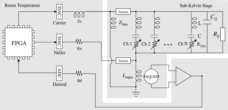
The circuit diagram of the TES array and the multiplexed readout is shown in Figure 1. The cold integrated fMux module (CIMM [29]), including the TES array with normal resistance and critical temperature (fabricated by commercial superconductor electronics fabrication facility (SeeQC [30])), a 40 channel LC resonator (fabricated at LBNL microsystem Laboratory [31]), a 112-junction series SQUID array amplifier (from STAR Cryoelectronics [32]), is mounted on a PC board with an A4K -metal magnetic shield inside an aluminum box, which is installed on the cold stage of a dilution refrigerator. The warm electronics is a DfMux version of the ICE readout electronics [33], with a field programmable gate array (FPGA) to synthesize the carrier and nuller, and to demodulate the signal from the SQUID. Digital Active Nulling (DAN [34]) is used to linearize the SQUID response and suppress the input impedance of the SQUID.
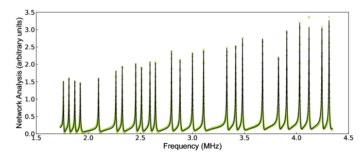
From the network analysis we find global parameters of the DfMux circuit, i.e. , , , , , and resonance frequencies for LC combs (, ). The inductance value for LC comb is designed to be and fixed as a known parameter in the analysis. Figure 2 shows the network analysis data and fit with circuit model. The DfMux circuit model for network analysis () is defined as , where
| (1) |
is the complex impedance of the DfMux circuit.
3 Theory on Sideband Complex ETF Response
The TES is held in transition with a voltage bias at carrier frequency , while an upper sideband is supplied at frequency . In practice, there is not a stiff voltage bias across the TES and rather its voltage bias can be analyzed as a Thévenin equivalent circuit which includes a phase shift caused by series impedance. However, here we assume perfect voltage bias given by , and a sideband which is a small fraction of the bias voltage are supplied to the TES, and apply a complex renormalization to the model transfer function in the end. We have chosen as we empirically found it to provide satisfactory signal-to-noise ratio while avoiding non-linearity. The sideband alternates between constructively and destructively interfering with the carrier, causing power modulation at frequency . The resistance responds to this power modulation with some time lag. This causes the demodulated sideband current and voltage to have a frequency-dependent relation in both amplitude and phase. This current-to-voltage transfer function is what we call the complex ETF response.
Assuming a small time-varying perturbation is produced in TES voltage, and the TES resistance changes by accordingly. The TES current , can be expanded and reduced to
| (2) |
Defining as the TES temperature sensitivity, and as the TES current sensitivity, the small change in TES resistance can be written as . Assuming that the TES joule power dissipation is in balance with the thermal heat flowing to the heat bath, we have the power-balance equation:
| (3) |
Expand equation (3) to first order and substitute , we get
| (4) |
where denotes for the thermal conductance between the TES and heat bath, and denotes for the heat capacity of the TES.
Given that the TES is biased by the carrier at frequency , the small change in resistance is only varied by the time-averaging power modulation as a result of the sideband interference. Combining equation (2) and (4) we can obtain
| (5) |
where , is the loop gain of the electrothermal feedback, is the electrical power dissipation on TES, and is the intrinsic time constant. Take the expression for carrier voltage bias and sideband into equation (5), we find it reduces to . Substituting into equation (2), we arrive at the expression for the current responses in the upper and lower sidebands, . The final form of TES complex ETF response including DfMux circuit transfer function is
| (6) |
/ for upper/lower sideband, respectively. refers to the complex impedance of the DfMux circuit as defined in equation (1). Note that in this case, R refers to the TES resistance of the channel of which sideband power modulation is applied, and TES resistances of other channels are set as the values they are under their own bias conditions (in our case they are set to zeros).
An additional phase calibration is necessary for the complex ETF response measurement, due to the fact that the current implementation of the DfMux system does not provide timestamp or reference associated with the zero-point of the phase in the carrier waveform. We perform this calibration by driving the TES to its normal state. A phase rotation is then divided from both the upper and lower sideband complex ETF responses. Be aware that there is no concept of phase-difference of the lower sideband current response relative to the upper sideband voltage bias since the lower and upper sideband are running on different frequencies, and . But since here the lower sideband is triggered simultaneously with the upper sideband, and the lower and upper sideband frequency are symmetric relative to the carrier, the initial phase of the lower sideband can be identified as the opposite to the reference phase in the upper sideband. In practice, we find that there is a small residual phase delay that is not accurately captured by this phase calibration method. However, this residual phase delay is captured by the complex normalization prefactor in the model.
4 Complex ETF Response Measurement and Data Fit
In complex ETF response measurement, we supply a bias voltage at carrier frequency centered at the LC resonance peak and a sideband , sweep the frequency from to , and measure the demodulated in-phase and quadrature current and . For phase calibration, we first drive the TES to the normal state with a large bias amplitude and fit for an initial phase from the time-ordered and data:
| (7) | |||
| (8) |
is the current amplitude measured at the carrier frequency when TES is in normal state, is the current amplitude measured for the sideband frequency when TES is normal state, and indicates the discrete time stamp. When TES is in transition, we observe both upper and lower sideband responses in the and data and a simultaneous fit is needed to determine their phase rotations:
| (9) | |||
| (10) |
is the current amplitude measured at the carrier frequency when TES is in superconducting transition state, and are the current amplitudes measured for upper and lower sidebands, respectively, when TES is in superconducting transition state. The upper and lower sideband complex response is defined as , and . Controlling the bath temperature to walk the TES through its superconducting transition, we measured the complex responses at for multiple depths in transition.
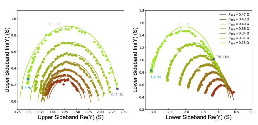
We fit the upper and lower sideband complex ETF responses datasets taken at various with model described in section 3 by minimizing the function, which is the square summation of measured upper and lower sideband TES complex ETF response minus the model divided by average noise level of the data. Figure 3 shows measured data and model fits for and in the complex plane.
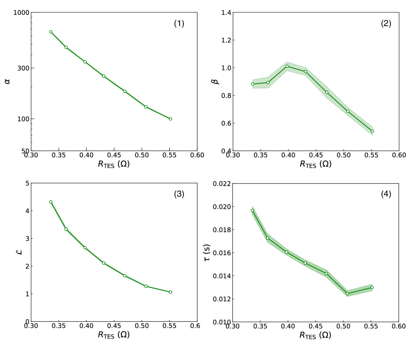
The , , and are variable for different TES resistances , while the DfMux circuit parameters, , , , and capacitance of the LC filter , are global parameters in the fitting procedure. In order to determine the statistical uncertainties, we use a bootstrap resampling method; the standard deviations are calculated from 100 datasets that were resampled with replacement. The best-fit parameters and the uncertainties estimated by bootstrapping are shown in Figure 4. When performing simultaneous fitting for the upper and lower sideband complex response data, we find a small phase correction is in need applying to and with opposite signs, i.e. . This uncertainty may be introduced via any common-mode error in determining and when fitting to the time-ordered data and . We also tried to incorporate a DAN transfer function prefactor of the form . This did not improve the fit significantly, indicating that this additional model complexity is not necessary for this work.
The best-fit equivalent circuit parameters for this TES are , , , . Those numbers are not exactly equal to what are derived from network analysis as shown at the end of section (2). This is because that the circuit parameters fit with network analysis is globally optimized for all channels, and the measurement was done with open-loop setup, where no digital active nulling feedback is enabled. On the contrary, during the complex ETF response measurement, the digital active nulling feedback is turned on so that the TES is effectively voltage biased, and the equivalent circuit parameters we extract from this measurement is dedicated for the specific channel being tested. Therefore, in terms of modelling the complex response of the TES under constant voltage bias condition, the equivalent circuit parameters estimated with this method should be more accurate and reliable than the network analysis.
Figure 4 shows the best-fit TES parameters as a function of depth in transition, including the loop gain , time constant , current sensitivity , and temperature sensitivity , which is calculated from . The thermal conductance was measured independently from the curves by fitting the at the same point where current sensitivity is negligible. The best fit results are nW/K, mK, and . With the time constant measured stably in the TES resistance range 0.350.55 from complex ETF response, we estimate the heat capacity of the bolometer is 1.21.6 pJ/K. The measured time constant, thermal conductance, and heat capacity are consistent with the designed values [35, 36]. The temperature in TES is calculated according to the thermal conductance function and . In our companion paper, we have also compared the loop gain, an effective indicator of , derived from the complex ETF response and that derived from the measurement, and confirmed that both methods yield consistent results at higher bias points where the constant voltage bias condition is still conserved [28]. The current sensitivity is quite small from this measurement, which is also consistent with the direct derivation of curves indicating that is not significantly larger than one or two for this type of TES.
The fit of simultaneous modeling the upper and lower sideband data is not perfect yet, due to the fact that full description of the circuit is very challenging, and further researches are still needed to solve the remaining issues in the fitting. Even though, we argue that the current result should still be able to provide a less biased measure of detector properties compared to single sideband fitting. In fact, we found that our current model can achieve better phenomenological fit to either upper sideband data or lower sideband data alone, without fitting to the other sideband. Comparing the differences in fit parameters considering either or both sidebands can give us an estimation of the systematic bias for this method. We found 0.1% difference in the LC filter capacitance, 10% difference in TES time constant, 10% difference in TES loop gain, and 6% difference in TES current sensitivity. Our method is therefore effective within in this confidence interval, and the fit parameters with both sidebands should give us the least systematically biased estimation. Moreover, the model enables us to further study relevant systematic errors of the detector calibration. For example, assuming the carrier frequency misaligned with the resonance peak frequency by 10 ppm, i.e. 20 Hz deviation from 2 MHz, can lead to 1% error in the loop gain and temperature sensitivity measurement, 4% error in the current sensitivity measurement, and 2% error in the time constant measurement. Such errors can be detrimental to experiments aiming for unprecedented precision, like the proposed LiteBIRD satellite mission.
5 Conclusion
We propose a novel method for modeling and characterizing the TES properties with the frequency-domain multiplexed readout using single sideband power modulation. The experiment confirms that TES complex ETF response in lower and upper sideband can be determined from the in-phase and quadrature current. A theoretical model includes both TES complex ETF response and DfMux circuit transfer function is derived under asymmetric sideband power modulation condition. The verification of this model is still in a beginning phase. First trials practicing the fit to sideband complex responses suggests the method could yield good estimation of the TES loop gain, time constant, temperature sensitivity, current sensitivity, and circuit parameters of the multiplexed readout circuit. Future efforts such as comparing the independent measurements of detector and circuit properties with the parameters fitted from the united model is still needed to justify the proposed method. If demonstrated to be effective, the method is potentially very useful in modeling the complex response of TESs in frequency-domain multiplexed readout, evaluating cross-talk and current leakage between adjacent channels, investigating the impact from any mismatch of carrier and resonance frequency, which are essentially valuable for understanding the systematics of experiments like the upcoming LiteBIRD CMB satellite project.
References
- \bibcommenthead
- [1] Irwin, K. D. & Hilton, G. C. Transition-Edge Sensors, Vol. 99, 63 (Springer, 2005).
- [2] Benford, D. J. The SOFIA/SAFIRE Far-Infrared Spectrometer: Highlighting Submillimeter Astrophysics and Technology. Submillimeter Astrophysics and Technology: a Symposium Honoring Thomas G. Phillips 417, 137 (2009).
- [3] Kelley, R. L. et al. The X-Ray Microcalorimeter Spectrometer for the International X-Ray Observatory. The Thirteenth International Workshop on Low Temperature Detectors - LTD13 1185, 757–760 (2009).
- [4] Horansky, R. D. et al. Superconducting calorimetric alpha particle sensors for nuclear nonproliferation applications. Applied Physics Letters 93, 123504 (2008).
- [5] Horansky, R. D. et al. Analysis of Nuclear Material by Alpha Spectroscopy with a Transition-Edge Microcalorimeter. Journal of Low Temperature Physics 151, 1067–1073 (2008).
- [6] Bacrania, M. K. et al. Large-Area Microcalorimeter Detectors for Ultra-High-Resolution X-Ray and Gamma-Ray Spectroscopy. IEEE Transactions on Nuclear Science 56, 2299–2302 (2009).
- [7] Rosenberg, D. et al. Long-Distance Decoy-State Quantum Key Distribution in Optical Fiber. PhysRevLett 98, 010503 (2007).
- [8] Miller, A. J., Nam, S. W., Martinis, J. M. & Sergienko, A. V. Demonstration of a low-noise near-infrared photon counter with multiphoton discrimination. Applied Physics Letters 83, 791 (2003).
- [9] Vaccaro, D. et al. Frequency domain multiplexing readout for large arrays of transition-edge sensors. Nuclear Instruments and Methods in Physics Research A 1046, 167727 (2023).
- [10] Bender, A. N. et al. On-Sky Performance of the SPT-3G Frequency-Domain Multiplexed Readout. Journal of Low Temperature Physics 199, 182–191 (2020).
- [11] Asavanant, W. et al. Time-Domain-Multiplexed Measurement-Based Quantum Operations with 25-MHz Clock Frequency. Physical Review Applied 16, 034005 (2021).
- [12] Akamatsu, H. et al. Demonstration of MHz frequency domain multiplexing readout of 37 transition edge sensors for high-resolution x-ray imaging spectrometers. Applied Physics Letters 119, 182601 (2021).
- [13] Dobbs, M. et al. Multiplexed readout of CMB polarimeters. Journal of Physics Conference Series 155, 012004 (2009).
- [14] LiteBIRD Collaboration et al. Probing cosmic inflation with the LiteBIRD cosmic microwave background polarization survey. Progress of Theoretical and Experimental Physics 2023, 042F01 (2023).
- [15] Lindeman, M. A. et al. Impedance measurements and modeling of a transition-edge-sensor calorimeter. Review of Scientific Instruments 75, 1283–1289 (2004).
- [16] Lindeman, M. A. et al. Complex Impedance and Equivalent Bolometer Analysis of a Low Noise Bolometer for SAFARI. Journal of Low Temperature Physics 167, 96–101 (2012).
- [17] Zhou, Y. et al. Mapping TES Temperature Sensitivity and Current Sensitivity as a Function of Temperature, Current, and Magnetic Field with IV Curve and Complex Admittance Measurements. Journal of Low Temperature Physics 193, 321–327 (2018).
- [18] Zhou, Y. Towards Understanding the Temperature and Current Sensitivities of Transition-Edge Sensors. Journal of Physics Conference Series 1590, 012032 (2020).
- [19] Martino, J. et al. Complementary Measurement of Thermal Architecture of NbSi TES with Alpha Particle and Complex Impedance. Journal of Low Temperature Physics 176, 350–355 (2014).
- [20] Takei, Y. et al. Characterization of a High-Performance Ti/Au TES Microcalorimeter with a Central Cu Absorber. Journal of Low Temperature Physics 151, 161–166 (2008).
- [21] Goldie, D. J., Audley, M. D., Glowacka, D. M., Tsaneva, V. N. & Withington, S. Thermal models and noise in transition edge sensors. Journal of Applied Physics 105, 074512–074512–7 (2009).
- [22] Galeazzi, M. & McCammon, D. Microcalorimeter and bolometer model. Journal of Applied Physics 93, 4856–4869 (2003).
- [23] Kinnunen, K. M., Palosaari, M. R. J. & Maasilta, I. J. Normal metal-superconductor decoupling as a source of thermal fluctuation noise in transition-edge sensors. Journal of Applied Physics 112, 034515–034515–10 (2012).
- [24] Palosaari, M. R. J. et al. Analysis of Impedance and Noise Data of an X-Ray Transition-Edge Sensor Using Complex Thermal Models. Journal of Low Temperature Physics 167, 129–134 (2012).
- [25] Akamatsu, H. et al. Impedance measurement and excess-noise behavior of a Ti/Au bilayer TES calorimeter. The Thirteenth International Workshop on Low Temperature Detectors 1185, 195–198 (2009).
- [26] Irwin, K. D. An application of electrothermal feedback for high resolution cryogenic particle detection. Applied Physics Letters 66, 1998–2000 (1995).
- [27] Taralli, E. et al. Complex impedance of TESs under AC bias using FDM readout system. AIP Advances 9, 045324 (2019).
- [28] de Haan, T. et al. Monitoring TES Loop Gain in Frequency Multiplexed Readout. JLTP, in preparation (2023).
- [29] de Haan, T. et al. Recent Advances in Frequency-Multiplexed TES Readout: Vastly Reduced Parasitics and an Increase in Multiplexing Factor with Sub-Kelvin SQUIDs. Journal of Low Temperature Physics 199, 754–761 (2020).
- [30] Suzuki, A. et al. Commercially Fabricated Antenna-Coupled Transition Edge Sensor Bolometer Detectors for Next-Generation Cosmic Microwave Background Polarimetry Experiment. Journal of Low Temperature Physics 199, 1158–1166 (2020).
- [31] Rotermund, K. et al. Planar Lithographed Superconducting LC Resonators for Frequency-Domain Multiplexed Readout Systems. Journal of Low Temperature Physics 184, 486–491 (2016).
- [32] Boyd, S. T. P., Groh, J. C., Hall, J. A., Suzuki, A. & Cantor, R. Series SQUID Array Amplifiers Optimized for MHz Frequency-Domain Multiplexed Detector Readout. The 17th International Workshop on Low-Temperature Detectors (2017).
- [33] Bandura, K. et al. ICE: A Scalable, Low-Cost FPGA-Based Telescope Signal Processing and Networking System. Journal of Astronomical Instrumentation 5, 1641005 (2016).
- [34] de Haan, T., Smecher, G. & Dobbs, M. Improved performance of TES bolometers using digital feedback. Millimeter, Submillimeter, and Far-Infrared Detectors and Instrumentation for Astronomy VI 8452, 84520E (2012).
- [35] Westbrook, B. et al. The POLARBEAR-2 and Simons Array Focal Plane Fabrication Status. Journal of Low Temperature Physics 193, 758–770 (2018).
- [36] Suzuki, A. Multichroic Bolometric Detector Architecture for Cosmic Microwave Background Polarimetry Experiments. Ph.D. thesis, University of California, Berkeley (2013).