Atomically thin obstructed atomic insulators with robust edge modes and quantized spin Hall effect
Abstract
Symmetry-protected edge states serve as direct evidence of nontrivial electronic topology in atomically thin materials. Finding these states in experimentally realizable single-phase materials presents a substantial challenge for their use for both fundamental studies and developing functional nanoscale devices. Here, we show the presence of robust edge states in phosphorene and group-Va monolayers with puckered lattice structures. By carefully analyzing the symmetry of the atomic sites and edge modes properties, we demonstrate that these atomically thin two-dimensional (2D) materials realize recently introduced obstructed atomic insulator states with partially occupied edge modes. The obstructed edge modes attain a Rashba-type spin splitting with Rashba parameter () of 1.52 eV Å for arsenene. Under strain or doping effects, these obstructed insulators transition to a phase with substantial spin-Berry curvature, yielding a double quantum spin Hall state with a spin Hall conductivity of 4. The experimental availability of phosphorene and other group-Va materials featuring puckered lattice structures could enable verification of obstructed atomic states and enhanced spin-Berry curvature effects discussed in this study, offering the potential for applications in topological electronic and spintronic devices.
Introduction. Coupling of electron topology, spin, and orbital degrees of freedom is the foundation of topological quantum materials having desirable disorder-resistant states [1, 2, 3]. The nontrivial topological state is generally driven by a bulk band inversion at high symmetry points in the Brillouin zone (BZ) and thus, the information of electronic wavefunction symmetries at these high-symmetry points is enough to diagnose the topology of a material as proposed in theory of topological quantum chemistry or symmetry indicators [4, 5, 6, 7]. Especially, within topological quantum chemistry, the band representations (BRs) of occupied states of a material can be expressed as a linear combination of the elementary band representations (eBRs, also known as the basis of atomic limit) at high-symmetry points. When specific coefficients of this linear combination of eBRs are rational fractions, the material is a topological insulator or topological semimetal. Conversely, if these coefficients are non-negative integers, the material is a trivial insulator [7, 8, 9, 10]. The topologically trivial insulators can also support unconventional surface states if their electrons occupy atom-unoccupied Wyckoff positions such that the BRs cannot be induced only from atom-centered band representations (aBRs) [11, 12, 13]. Such insulators, dubbed as obstructed atomic insulators (OAIs), host electronic states with filling anomaly at surfaces cleaved at atom-unoccupied Wyckoff positions [13]. The OAIs have been predicted in three-dimensional (3D) materials and verified recently in SrIn2P2 and elemental silicon [14, 15]. The OAIs hold great promise for realizing exotic states such as higher-order topological states, unconventional superconductivity, and electrides with superior catalytic properties useful for quantum science and technological applications [16, 17, 18, 19, 20, 21, 22, 23, 24].
The atomically thin 2D materials provide an unprecedented framework for investigating topological quantum phenomena under carrier confinement that can be further manipulated by external strain, electric field, and/or doping effects [25, 26, 27, 28]. Among various families of 2D materials, phosphorene and group-Va materials with puckered honeycomb lattice are mechanically exfoliated to the monolayer limit [27, 28, 29, 30, 31, 32, 33]. They show a thickness-dependent bandgap which is further sensitive to external electric field and surface doping effects. Specifically, a topologically nontrivial Dirac semimetal state is realized in phosphorene via potassium surface doping or under a vertical electric field [34, 35, 36, 37]. The other group-Va monolayer layers as one moves down the periodic table (PAsSb) show a topological phase transition to a state with multiple unpinned Dirac cones and puzzling intertwining edge states [33, 38, 39]. Despite these studies, it is unclear if these 2D materials can support OAIs with conducting edge modes, and how the edge modes evolve across the periodic table in these materials.
In this paper, we report the theoretical prediction of the OAI state with spin-filtered edge modes in monolayers of group-Va materials with puckered honeycomb lattice. Through a systematic analysis of the bulk and edge energy spectra combined with symmetry analysis, we illustrate that phosphorene and group-Va monolayers exhibit half-filled obstructed states along both armchair and zigzag edges. The obstructed edge states (OESs) exhibit a finite Rashba-type spin-splitting with a Rashba coupling constant of eV Å for Arsenene. We discuss the evolution of OESs from P to As and Sb and show that due to a generic point band inversion in Sb, these states evolve to form gapless double quantum spin Hall states in Sb with quantized spin Hall conductivity of . Such topological phase transition can be captured by applying uniaxial strain in Arsenene. We further demonstrate that these materials respect spin U(1) quasi-symmetry which ascertains a quantized spin Hall conductivity and two pairs of spin-polarized counter-propagating topological edge states.
Crystal structure and OAI identification. We start discussing the puckered honeycomb structure of phosphorene, which is a single layer of bulk black phosphorus. Phosphorene consists of two stacked P zigzag chains such that each P atom forms three bonds with its nearest neighbor atoms (Fig. 1(a)). Such a bonding configuration drives a non-symmorphic space group (). It respects inversion , a vertical mirror plane perpendicular to the zigzag direction and two-fold rotations , , and glide mirror and symmetries. P atoms occupy Wyckoff position in the lattice that induces 4 (8) BRs of single (double) space group. There are two additional Wyckoff positions and in lattice that are not occupied by atoms. Considering 5 valence electrons of P and any group-Va element, the phosphorene lattice has 20 valence electrons. This satisfies a condition for filling-enforced OAI, , where , for space group P [11]. This implies that the decomposition of BR into eBRs should include BRs generated from atom-unoccupied Wyckoff positions.
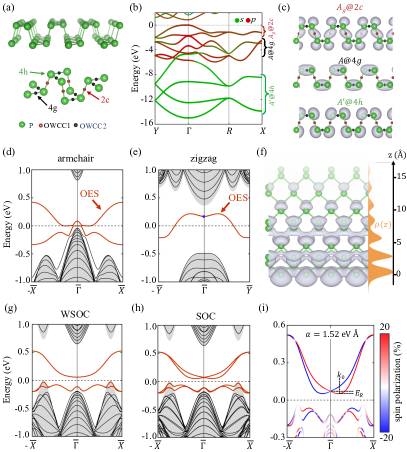
To identify the BRs of unoccupied Wyckoff positions, we present the band structure of phosphorene in Fig. 1(b) (see SMs for calculational details). The valence and conduction bands are well separated with an energy gap, dictating an insulator ground state. A mapping of irreducible representations (IRs) of occupied bands by considering the eBRs of single-space group reveals that bands belong to BRs induced from atom-occupied Wyckoff position (marked as in Fig. 1(b)). The remaining -type bands belong to BRs that are generated from atom-unoccupied Wyckoff positions and ( and ). This is more resolved in real-space charge localization of band representations in Fig. 1(c). Specifically, the electronic charge density distribution arising from BRs of and at point are localized on the empty Wyckoff positions and , respectively. In contrast, the charge density of states is centered at atom-occupied Wyckoff position . The bands with orbital character in phosphorene thus arise from unoccupied or obstructed atomic sites in the lattice.
We further evaluate the single-valued real space invariant (RSI) at Wyckoff positions , , and of space group to elucidate the OAI state [13]. The RSI index at each Wyckoff position is defined as , , and , where is the number of eBRs () induced from a Wyckoff position. We obtain , , and . The non-zero integer values of RSI at and confirm the OAI phase in phosphorene. A similar analysis holds for all other group-Va monolayers with a puckered lattice. The nontrivial RSI index indicates that these monolayers will support robust states over edges that cut through unoccupied Wyckoff positions.
In Figs. 1(d) and 1(e), we present the first-principles edge band structure of phosphorene terminated at (zigzag edge) and (armchair edge) sites without SOC. Both edges support the partially filled conducting states within the 2D bulk energy gap. Notably, the OESs do not connect the bulk valence and conduction bands and thus, are distinct from quantum spin Hall insulators where the helical edge states connect the bulk valence and conduction bands. Regardless, the OESs cross the Fermi level, exhibiting the filling anomaly [11, 12, 13]. Figure 1(f) illustrates the distribution of the electronic charge density associated with OESs at point for the zigzag edge and its variation as a function of slab thickness (). The electronic charge density is localized at the slab edge and decays exponentially into the bulk as expected for edge states. We further show the OESs of arsenene in Figs. 1(g)-1(i). Due to a slightly larger SOC, the OESs in Arsenene are spin-polarized with SOC. They show a Rashba-type spin splitting with maximum energy offset of eV at Å-1 with a Rashba constant eVÅ.
Hidden structural and topological phase transition. We now discuss the evolution of electronic structure from monolayer P to Sb and reveal a unique topological phase transition. In Figs. 2(a)-2(c), we present the orbital-resolved band structures of these monolayers in the vicinity of the Fermi level. Although the band structure stays insulating from P to Sb along the high-symmetry directions, there are subtle changes in it. The valence and conduction band extremum is shifted from the point in P to a generic momentum point in Sb. The bands consist of orbital at the point whereas they are comprised of orbitals along direction. These bands change dispersion from parabolic in P and As to almost linear and gapless in Sb. Figure 2(d) illustrates the energy dispersion of Sb in the full 2D BZ. Interestingly, the bands remain gapless across the line, forming four Dirac cones on the plane. These Dirac cones are located at generic momenta as resolved in the constant energy contours in Fig. 2(e). The SOC effects open a hybridization gap at the Dirac nodes, leading to an inverted band structure with band inversion at generic points (Fig. 2(f)).
In Fig. 2(g), we present the wannier charge centers (WCCs) spectrum of the occupied states of P and Sb. The WCCs spectrum shows adiabatically distinct characteristics, remaining gapful for P and gapless for Sb. Despite these features, the WCCs spectrum reveals trivial connectivity for both P and Sb, thereby dictating a trivial state. The topological trivial state is further verified through the parity analysis of occupied bands at high-symmetry points. The presence of a band inversion and the WCCs connectivity in Sb signals a nontrivial electronic state distinct from P. However, since the band inversion happens at generic points, it does not alter IRs of occupied bands at the high-symmetry points. Such a topological state is hidden from symmetry-indicator and TQC theories, and therefore, P, As, and Sb share the same topological characterization [38, 39].
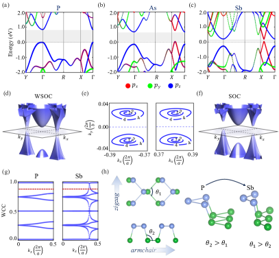
We emphasize that the emergence of electronic structure from P to Sb has a strong correlation with their puckered lattice geometry and signals a hidden structural transition. To facilitate this analysis, we define bond angles and in the puckered lattice as shown in Fig. 2(h). is an in-plane angle in the zigzag layer and is the out-of-plane angle along the armchair direction, describing the non-planner puckering of the lattice. and are and for P and and for Sb, respectively. This indicates that the in-plane bond angle is smaller than the non-planner bond angle () for P with less puckering. This bond angle order is reversed for Sb with with large puckering. The electronic phase transition happens when . Importantly, when , each atom shares an isotropic electronic environment similar to graphene, thereby forming two critical points on the line without SOC. When , each critical point splits into two Dirac points across the line as seen in Sb.
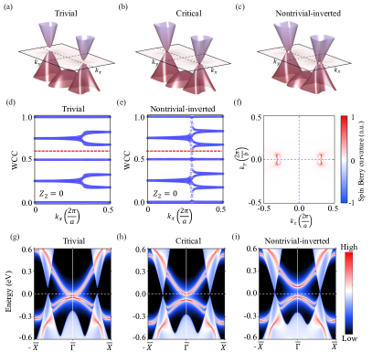
A similar topological phase transition can also happen in As under the application of uniaxial strain along the zigzag direction. In Figs. 3(a)-3(c), we present the calculated band structure of As at various values of strain. We change the lattice parameter along the zigzag direction (see SM for details). When , the valence and conduction bands have a parabolic energy dispersion with minimum along direction. With an increase in , the valence and conduction bands start approaching each other and cross at line for (Fig. 3(b)). With a further increase in , four Dirac cones appear at the generic points across the line. In Figs. 3(d)-3(e), we present WCCs spectrum of As for and with SOC. The WCCs spectrum resolves distinct characteristics with a trivial phase. However, a strong spin-Berry curvature is found near the gapped Dirac nodes for As with generic point band inversion (Fig. 3(f)).
To explore the emergence of OESs with strain, we present the calculated armchair edge spectrum in Figs. 3(g)-3(i) for , , and . The two pairs of OESs are seen within the bulk gap in the vicinity of the Fermi level for (Fig. 3(g)). These OESs evolve to form gapless Dirac-type states within the bulk band inversion at generic points, forming double quantum spin-Hall edge states.
Helical spin-texture and quantized spin Hall effect. The preceding discussion made it clear that although Sb or strained As are OAIs based on the analysis of IRs at high-symmetry points, they host a topologically distinct band structure than P or As. Their OESs form a gapless Dirac-type energy dispersion within the bulk gap. In Figs. 4(a)-4(b), we show the spin texture of these edge states for Sb and As with . The two pairs of oppositely spin-polarized edge states are evident along - direction. They have a dominant spin component and thus, preserve a spin U(1) quasi-symmetry (see SMs). Notably, owing to the presence of time-reversal symmetry and symmetry along the armchair edge, the edge states can support both and spin components. However, we find that here is negligible. Such spin-symmetry leads to gapless edge states and can support perfectly quantized spin Hall conductivity. In Fig. 4(c), we show a schematic representation of the gapless Dirac-type edge states as seen in Sb or strained As with .
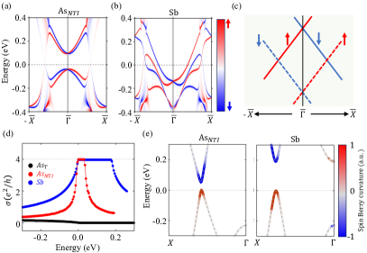
Figure 4(d) illustrates the calculated intrinsic spin Hall conductivity (SHC) as a function of the Fermi energy for As and Sb. The SHC is calculated using the Kubo formula [40, 41]. Here, is the -resolved spin Berry curvature and gives the band resolved spin Berry curvature in 2D BZ with area . represents the energy of Bloch state with occupation . The spin current operator is defined as , where is the spin operator and is the velocity operator. represents -polarized spin-current along direction generated by an electric field along direction. The SHC for the As is zero, whereas it has a quantized value of for Sb and strained As () in the bulk gap region. Such a large SHC arises due to strong spin-Berry curvature at the band inverted points in both Sb and AsNTI (Fig. 4(e)).
Generally, the SHC deviates from exact quantization due to nonconserved- Hamiltonians in materials [42, 43, 44, 45]. However, as shown in Ref. [38], the group-Va monolayers host a unique SOC Hamiltonian , where is momentum around Dirac node and and are Pauli matrices acting on orbital and spin space. This commutes with Sz, leading to a spin U(1) quasi-symmetry and perfect quantization of SHC as found here. Owing to the presence of SOC Hamiltonian preserving spin U(1) quasi-symmetry, the associated topological state can be described by a spin-Chern number of 2 [43, 44, 45, 46].
Summary. We demonstrate the presence of OAI state in phosphorene and related group-Va monolayers with a puckered lattice. The charge density of their occupied bands near the Fermi level is centered at atom-unoccupied Wyckoff positions. Such localization of charge centers leads to nontrivial RSI index and OESs on crystal edges that cut through the unoccupied Wyckoff positions. We show that OESs are spin-polarized for As having a Rashba-type spin splitting with Rashba parameter of 1.52 eV Å. We resolve a unique topological state with generic points band inversion in Sb and strained As and perfectly quantized SHC of . We argue that the perfect quantization of SHC arises because of a unique conserved SOC Hamiltonian. Our work demonstrates that phosphorene and other group-Va monolayers would provide an ideal basis for exploring OAIs and enhanced spin-Berry curvature effects with potential applications in topological spintronics.
Acknowledgements. We thank Bikash Patra for the useful discussions. This work is supported by the Department of Atomic Energy of the Government of India under Project No. 12-RD-TFR-5.10-0100 and benefited from the HPC resources of TIFR Mumbai.
References
- Hasan and Kane [2010] M. Z. Hasan and C. L. Kane, Colloquium: Topological insulators, Rev. Mod. Phys. 82, 3045 (2010).
- Tokura et al. [2017] Y. Tokura, M. Kawasaki, and N. Nagaosa, Emergent functions of quantum materials, Nat. Phys. 13, 1056 (2017).
- Singh et al. [2022] B. Singh, H. Lin, and A. Bansil, Topology and symmetry in quantum materials, Adv. Mater. 35, 2201058 (2022).
- Kruthoff et al. [2017] J. Kruthoff, J. de Boer, J. van Wezel, C. L. Kane, and R.-J. Slager, Topological classification of crystalline insulators through band structure combinatorics, Phys. Rev. X 7, 041069 (2017).
- Po et al. [2017] H. C. Po, A. Vishwanath, and H. Watanabe, Symmetry-based indicators of band topology in the 230 space groups, Nat. Commun. 8, 50 (2017).
- Song et al. [2018] Z. Song, T. Zhang, Z. Fang, and C. Fang, Quantitative mappings between symmetry and topology in solids, Nat. Commun. 9, 3530 (2018).
- Bradlyn et al. [2017] B. Bradlyn, L. Elcoro, J. Cano, M. G. Vergniory, Z. Wang, C. Felser, M. I. Aroyo, and B. A. Bernevig, Topological quantum chemistry, Nature 547, 298 (2017).
- Michel [2001] L. Michel, Elementary energy bands in crystals are connected, Phys. Rep. 341, 377 (2001).
- Cano et al. [2018a] J. Cano, B. Bradlyn, Z. Wang, L. Elcoro, M. G. Vergniory, C. Felser, M. I. Aroyo, and B. A. Bernevig, Building blocks of topological quantum chemistry: Elementary band representations, Phys. Rev. B 97, 035139 (2018a).
- Cano et al. [2018b] J. Cano, B. Bradlyn, Z. Wang, L. Elcoro, M. G. Vergniory, C. Felser, M. I. Aroyo, and B. A. Bernevig, Topology of disconnected elementary band representations, Phys. Rev. Lett. 120, 266401 (2018b).
- Xu et al. [2024] Y. Xu, L. Elcoro, Z.-D. Song, M. G. Vergniory, C. Felser, S. S. P. Parkin, N. Regnault, J. L. Mañes, and B. A. Bernevig, Filling-enforced obstructed atomic insulators, Phys. Rev. B 109, 165139 (2024).
- Gao et al. [2022] J. Gao, Y. Qian, H. Jia, Z. Guo, Z. Fang, M. Liu, H. Weng, and Z. Wang, Unconventional materials: the mismatch between electronic charge centers and atomic positions, Sci. Bull. 67, 598 (2022).
- Xu et al. [2021] Y. Xu, L. Elcoro, G. Li, Z.-D. Song, N. Regnault, Q. Yang, Y. Sun, S. Parkin, C. Felser, and B. A. Bernevig, Three-dimensional real space invariants, obstructed atomic insulators and a new principle for active catalytic sites, (2021), arXiv:2111.02433 .
- Liu et al. [2023] X.-R. Liu, H. Deng, Y. Liu, Z. Yin, C. Chen, Y.-P. Zhu, Y. Yang, Z. Jiang, Z. Liu, M. Ye, D. Shen, J.-X. Yin, K. Wang, Q. Liu, Y. Zhao, and C. Liu, Spectroscopic signature of obstructed surface states in SrIn2P2, Nat. Commun. 14, 2905 (2023).
- Chen et al. [2023] Y. Chen, Z. Liu, P. Deng, Y. Xu, H. Yang, D. Pei, C. Chen, S. He, D. Liu, S.-K. Mo, T. Kim, C. Cacho, H. Yao, Z. Song, X. Chen, Z. Wang, B. Yan, L. Yang, and B. Bernevig, Massive 1D Dirac line, solitons and reversible manipulation on the surface of a prototype obstructed atomic insulator, silicon 10.21203/rs.3.rs-2781859/v1 (2023).
- Ma et al. [2023] D.-S. Ma, K. Yu, X.-P. Li, X. Zhou, and R. Wang, Obstructed atomic insulators with robust corner modes, Phys. Rev. B 108, L100101 (2023).
- Benalcazar et al. [2019] W. A. Benalcazar, T. Li, and T. L. Hughes, Quantization of fractional corner charge in -symmetric higher-order topological crystalline insulators, Phys. Rev. B 99, 245151 (2019).
- Wang et al. [2022] L. Wang, Y. Jiang, J. Liu, S. Zhang, J. Li, P. Liu, Y. Sun, H. Weng, and X.-Q. Chen, Two-dimensional obstructed atomic insulators with fractional corner charge in the family, Phys. Rev. B 106, 155144 (2022).
- Sheng et al. [2023] H. Sheng, Y. Xie, Q. Wu, H. Weng, X. Dai, B. A. Bernevig, Z. Fang, and Z. Wang, Majorana corner modes in unconventional monolayers of family, (2023), arXiv:2308.12055 .
- Yang et al. [2023] Z. Yang, H. Sheng, Z. Guo, R. Zhang, Q. Wu, H. Weng, Z. Fang, and Z. Wang, Superconductivity in unconventional metals, (2023), arXiv:2306.08347 .
- Eck et al. [2022] P. Eck, C. Ortix, A. Consiglio, J. Erhardt, M. Bauernfeind, S. Moser, R. Claessen, D. Di Sante, and G. Sangiovanni, Real-space obstruction in quantum spin hall insulators, Phys. Rev. B 106, 195143 (2022).
- [22] G. Li, Y. Xu, Z. Song, Q. Yang, Y. Zhang, J. Liu, U. Gupta, V. Sub, Y. Sun, P. Sessi, S. S. P. Parkin, B. A. Bernevig, and C. Felser, Obstructed surface states as the descriptor for predicting catalytic active sites in inorganic crystalline materials, Adv. Mater. 34, 2201328.
- Nie et al. [2021] S. Nie, Y. Qian, J. Gao, Z. Fang, H. Weng, and Z. Wang, Application of topological quantum chemistry in electrides, Phys. Rev. B 103, 205133 (2021).
- Jiang et al. [2023] K. Jiang, Z. Qi, H. Weng, and J. Hu, Mottness in obstructed atomic insulators without mott transition, Phys. Rev. B 108, 195102 (2023).
- Novoselov et al. [2016] K. S. Novoselov, A. Mishchenko, A. Carvalho, and A. H. C. Neto, 2D materials and van der waals heterostructures, Science 353, aac9439 (2016).
- Sheng et al. [2021] F. Sheng, C. Hua, M. Cheng, J. Hu, X. Sun, Q. Tao, H. Lu, Y. Lu, M. Zhong, K. Watanabe, T. Taniguchi, Q. Xia, Z.-A. Xu, and Y. Zheng, Rashba valleys and quantum hall states in few-layer black arsenic, Nature 593, 56 (2021).
- Carvalho et al. [2016] A. Carvalho, M. Wang, X. Zhu, A. S. Rodin, H. Su, and A. H. Castro Neto, Phosphorene: from theory to applications, Nat Rev Mater 1, 1 (2016).
- Xia et al. [2019] F. Xia, H. Wang, J. C. M. Hwang, A. H. C. Neto, and L. Yang, Black phosphorus and its isoelectronic materials, Nat. Rev. Phys. 1, 306–317 (2019).
- Kim et al. [2015] J. Kim, S. S. Baik, S. H. Ryu, Y. Sohn, S. Park, B.-G. Park, J. Denlinger, Y. Yi, H. J. Choi, and K. S. Kim, Observation of tunable band gap and anisotropic dirac semimetal state in black phosphorus, Science 349, 723 (2015).
- Lu et al. [2021] Q. Lu, K. Y. Chen, M. Snyder, J. Cook, D. T. Nguyen, P. V. S. Reddy, T.-R. Chang, S. A. Yang, and G. Bian, Observation of symmetry-protected dirac states in nonsymmorphic -antimonene, Phys. Rev. B 104, L201105 (2021).
- Kowalczyk et al. [2020] P. J. Kowalczyk, S. A. Brown, T. Maerkl, Q. Lu, C.-K. Chiu, Y. Liu, S. A. Yang, X. Wang, I. Zasada, F. Genuzio, T. O. Menteş, A. Locatelli, T.-C. Chiang, and G. Bian, Realization of symmetry-enforced two-dimensional dirac fermions in nonsymmorphic -bismuthene, ACS Nano 14, 1888 (2020).
- Islam et al. [2021] R. Islam, B. Ghosh, C. Autieri, S. Chowdhury, A. Bansil, A. Agarwal, and B. Singh, Tunable spin polarization and electronic structure of bottom-up synthesized MoSi2N4 materials, Phys. Rev. B 104, L201112 (2021).
- Lu et al. [2022] Q. Lu, J. Cook, X. Zhang, K. Y. Chen, M. Snyder, D. T. Nguyen, P. V. S. Reddy, B. Qin, S. Zhan, L.-D. Zhao, P. J. Kowalczyk, S. A. Brown, T.-C. Chiang, S. A. Yang, T.-R. Chang, and G. Bian, Realization of unpinned two-dimensional dirac states in antimony atomic layers, Nat. Commun. 13, 4603 (2022).
- Ghosh et al. [2016] B. Ghosh, B. Singh, R. Prasad, and A. Agarwal, Electric-field tunable dirac semimetal state in phosphorene thin films, Phys. Rev. B 94, 205426 (2016).
- Baik et al. [2015] S. S. Baik, K. S. Kim, Y. Yi, and H. J. Choi, Emergence of two-dimensional massless dirac fermions, chiral pseudospins, and berry’s phase in potassium doped few-layer black phosphorus, Nano Lett. 15, 7788 (2015).
- Liu et al. [2015] Q. Liu, X. Zhang, L. B. Abdalla, A. Fazzio, and A. Zunger, Switching a normal insulator into a topological insulator via electric field with application to phosphorene, Nano Lett. 15, 1222 (2015).
- Xiang et al. [2015] Z. J. Xiang, G. J. Ye, C. Shang, B. Lei, N. Z. Wang, K. S. Yang, D. Y. Liu, F. B. Meng, X. G. Luo, L. J. Zou, Z. Sun, Y. Zhang, and X. H. Chen, Pressure-induced electronic transition in black phosphorus, Phys. Rev. Lett. 115, 186403 (2015).
- Lu et al. [2016] Y. Lu, D. Zhou, G. Chang, S. Guan, W. Chen, Y. Jiang, J. Jiang, X. sen Wang, S. A. Yang, Y. P. Feng, Y. Kawazoe, and H. Lin, Multiple unpinned dirac points in group-Va single-layers with phosphorene structure, Npj Comput. Mater. 2, 1 (2016).
- Wang et al. [2024] B. Wang, X. Zhou, Y.-C. Hung, Y.-C. Lin, H. Lin, and A. Bansil, High spin-chern-number insulator in -antimonene with a hidden topological phase, 2D Mater. 11, 025033 (2024).
- Sun et al. [2016] Y. Sun, Y. Zhang, C. Felser, and B. Yan, Strong intrinsic spin hall effect in the TaAs family of weyl semimetals, Phys. Rev. Lett. 117, 146403 (2016).
- Qiao et al. [2018] J. Qiao, J. Zhou, Z. Yuan, and W. Zhao, Calculation of intrinsic spin hall conductivity by wannier interpolation, Phys. Rev. B 98, 214402 (2018).
- Kane and Mele [2005] C. L. Kane and E. J. Mele, topological order and the quantum spin hall effect, Phys. Rev. Lett. 95, 146802 (2005).
- Sheng et al. [2006] D. N. Sheng, Z. Y. Weng, L. Sheng, and F. D. M. Haldane, Quantum spin-hall effect and topologically invariant chern numbers, Phys. Rev. Lett. 97, 036808 (2006).
- Prodan [2009] E. Prodan, Robustness of the spin-chern number, Phys. Rev. B 80, 125327 (2009).
- Sheng et al. [2005] L. Sheng, D. N. Sheng, C. S. Ting, and F. D. M. Haldane, Nondissipative spin hall effect via quantized edge transport, Phys. Rev. Lett. 95, 136602 (2005).
- Liu et al. [2024] L. Liu, Y. Liu, J. Li, H. Wu, and Q. Liu, Quantum spin hall effect protected by spin (1) quasi-symmetry, (2024), arXiv:2402.13974 .