Minimizing Kinetic Inductance in Tantalum-Based Superconducting Coplanar Waveguide Resonators for Alleviating Frequency Fluctuation Issues
Abstract
Advancements in the fabrication of superconducting quantum devices have highlighted tantalum as a promising material, owing to its low surface oxidation microwave loss at low temperatures. However, tantalum films exhibit significantly larger kinetic inductances compared to materials such as aluminum or niobium. Given the inevitable variations in film thickness, this increased kinetic inductance leads to considerable, uncontrolled frequency variances and shifts in components like superconducting coplanar waveguide resonators. Achieving high precision in resonator frequencies is crucial, particularly when multiple resonators share a common Purcell filter with limited bandwidth in superconducting quantum information processors. Here, we tackle this challenge from both fabrication and design perspectives, achieving a reduction in resonator frequency fluctuation by 100 fold. Concurrently, the internal quality factor of the superconducting coplanar waveguide resonator remains at high level. Our findings open up new avenues for the enhanced utilization of tantalum in large-scale superconducting chips.
I Introduction
Over the past two decades, significant advancements in device coherence times have propelled superconducting qubits to the forefront of quantum computing technology [1, 2]. The lifespan of planar transmon qubits, fabricated using tantalum (Ta), has been extended over 0.5ms [3, 4, 5]. Historically, research of superconducting materials has primarily focused on minimizing uncontrolled defect sites, which could potentially function as sources of two-level systems (TLS) [6, 7]. However, the kinetic inductance, another significant property of superconducting material, has received less attention in the context of superconducting quantum information processors.
In comparison to conventional superconducting materials like aluminum or niobium (Nb), Ta displays a higher kinetic inductance, depending on factors such as film thickness and temperature [8, 9]. The increased kinetic inductance, together with the thickness variation of magnetron-sputtered body-centered cubic or -Ta films, may lead to considerable uncontrolled superconducting coplanar waveguide (SCPW) resonator frequency fluctuations across the wafer [10, 11]. Such fluctuations present a significant challenge for large-scale circuit QED-based quantum information systems, as they can cause frequency crowding and cross-talk issues, particularly when multiple resonators share a limited-bandwidth common Purcell filter [12, 13].
Firstly, we will investigate the impact of kinetic inductance on the SCPW resonator frequency [14, 11]. In this study, a quarter-wavelength SCPW resonator is utilized, and its frequency is estimated as: , where denotes the SCPW length, and () represents the capacitance (inductance) per unit length. The magnetic field penetrates the superconductor to a depth governed by the penetration depth [15], as shown in Fig. 1(b). For an intuitive understanding, we can image that the supercurrent within this layer under the driving of a alternating filed will be accelerated and gain velocity and momentum. When the field is reversed, copper pairs in the supercurrent must first loose their momentum before changing direction. The current lags the field by 90∘ due to the kinetic energy stored within the copper pairs. That is inductance. Consequently, , where is the constant geometric component, corresponding to the magnetic energy outside the superconducting film, and is the variable kinetic component. Of course, there is also magnetic energy inside the superconducting film, but we find it will not change our optimization strategy, we will not consider it in this experimental study. Because there is an inevitable thickness variation when sputtering the Ta film depends on deposition system. Consequently, our main goal is to minimize , expecting a decrease in its variance and resonator frequency fluctuations with the same of the Ta film.
Next, we will clarify the elements influencing , and the methods to minimize it. As shown in Ref. [10], if is smaller than twice the magnetic penetration depth , the kinetic inductance can be approximated as:
| (1) |
where denotes the vacuum permeability, the SCPW’s center electrode width, the gap between the center and ground electrodes, as shown in Fig. 1(b), and a geometric factor. Although the assumption for this approximation may not always be valid in this study, the formula still provide an intuitive understanding of how reducing and optimizing the SCPW geometry can contribute to the minimization of .
To decrease , we can enhance the film thickness , as shown in studies on Nb and aluminum films [8, 16]. Also, increasing the substrate temperature during sputtering, which will lead to larger -Ta grain sizes [17, 9, 18], can also reduce . This is based on the idea that a larger grain size allows fewer disturbances in the superconducting current flow, behaving more like a bulk material, which usually has a smaller than a thin film. Besides fabrication optimization, can also be reduced by adjusting and from a design perspective. By applying these modifications, we achieve a more than 100-fold reduction in resonator frequency variation.
II Results
II.1 Device and Optimized Results
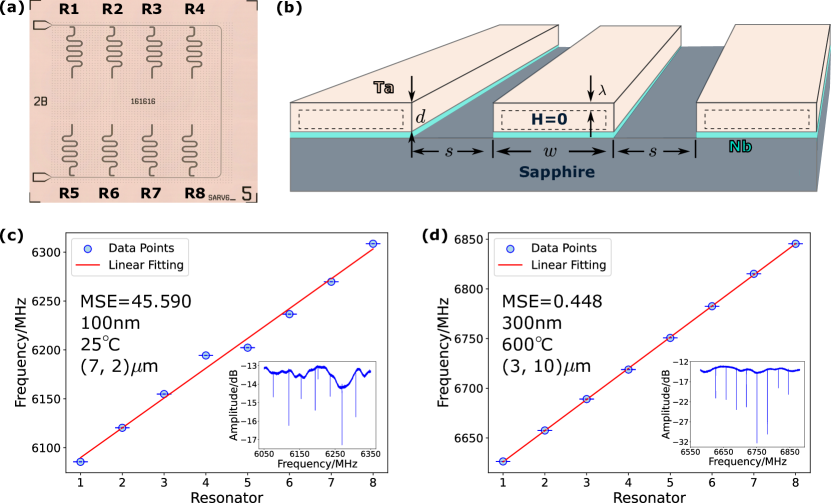
We begin by introducing the SCPW resonator design under investigation. As depicted in Fig. 1(a), eight resonators are coupled to a shared readout line. We add labels only in the figure for identification. The resonators’ frequencies are designed to follow a linear distribution, with an average frequency of 6.7 GHz and a 30 MHz frequency gap between each. The coupling quality factor of the resonators falls within the range of 0.5 to 1 million. All electromagnetic simulations are conducted with a frequency convergence precision of one percent, without considering the kinetic inductance. The relative permittivity of the sapphire substrate is set to 10.55 [19]. The internal quality factor and frequency of each resonator can be obtained by fitting their transmissive signal , measured from the readout line [20].
To quantify the resonator frequency variation, we opt for the mean square error (MSE) of the linear fit to the observed frequency distribution, rather than a traditional parameter like the standard deviation of a group of resonators with the same design frequency. MSE is defined as MSE=, where represents the number of data points, refers to the actual values, and denotes the predicted values. This approach is chosen due to the requirement for distinct frequencies among different resonators on the same readout line. As a result, we use MSE as an indicator of deviation from linearity, where a smaller value is desirable. Additionally, we compute the mean frequency shift relative to the design value 6.7 GHz to represent the relative amount of for various optimization parameters.
In Fig. 1(b), we show the cross section of the SCPW resonator. In our study, we also adjust the substrate temperature during sputtering to modify the grain size of the -Ta film. However, to ensure a high purity -Ta, previous studies [3, 4] have indicated that a high temperature for sapphire substrate is necessary. To address this challenge, we employ a 5 nm Nb buffer layer to get high purity phase of Ta for different temperatures [21], as illustrated in Fig. 1(b).
The pre-optimization results are displayed in Fig. 1(c). During this chip’s fabrication, we maintained the sapphire substrate temperature at room temperature, approximately 25∘C. The Ta film thickness was set to 100 nm, and the SCPW resonator structure had an of 7 m and a of 2 m. Blue points represent measured SCPW resonator frequencies, while error bars indicate one standard deviation of the fitting process of the transmissive coefficient . The subplot demonstrates the amplitude response of . From these measurements, we obtained an MSE of 45.590.
Fig. 1(d) presents SCPW resonator frequencies after optimization. We applied the following optimization methods: increasing the Ta film thickness to 300 nm, setting the sapphire substrate temperature to 600∘C during Ta film sputtering, and adjusting and to 3 m and 10 m for the SCPW resonator. All SCPW resonators are measured with the same condition with SCPW resonators in Fig. 1(c). These optimizations yielded an MSE of 0.448, signifying a more than 100-fold reduction in resonator frequency variation compared to the pre-optimization MSE. Additionally, utilizing these optimization methods, the discrepancy between the average measured frequencies of the resonators and the average frequencies of the designed resonators has been reduced from approximately -500 MHz to approximately +36 MHz. Despite the positive sign being attributed to the uncertainty of the sapphire permittivity during the SCPW resonator design process, this result signifies a fundamental reduction of .
II.2 Film Thickness Optimization
For the Ta film, the theoretical effective penetration depth can be represented as [8, 16]:
| (2) |
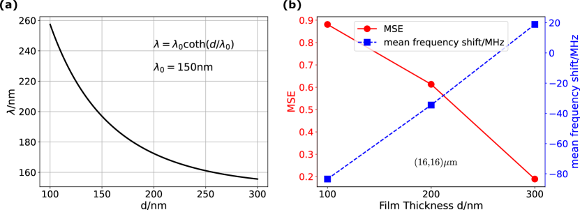
where =150nm is the penetration depth of bulk superconductor [22] and is the thickness of the film. The trend of the effective penetration depth changes in Ta films is illustrated in Fig. 2(a), where an increase in film thickness results in a decrease in effective penetration depth. As can be inferred from Eqn. 1, the increase in and the corresponding decrease in penetration depth contribute to a reduction in kinetic inductance. This is attributed to the fact that changes very slowly with . Consequently, kinetic inductance can be mitigated by increasing the film thickness.
Fig. 2(b) displays the MSE distribution for different samples with only film thickness as varying parameters. As the thickness of Ta films increases from 100 nm to 300 nm, the MSE decreases monotonically from about 0.9 to approximately 0.2, signifying a notable improvement in resonator frequency stability. Furthermore, we employ of SCPW resonators to examine the changes in kinetic inductance. Since , the change in from approximately -80 MHz to +20 MHz, relative to the designed frequency of 6.7 GHz, corresponds to a decreased as the Ta film thickness increases. The positive stems from the uncertainty in the permittivity of sapphire, which is set to 10.55 in the simulation and may be slightly higher than the actual value of the material used.
II.3 Sputtering Temperature Optimization
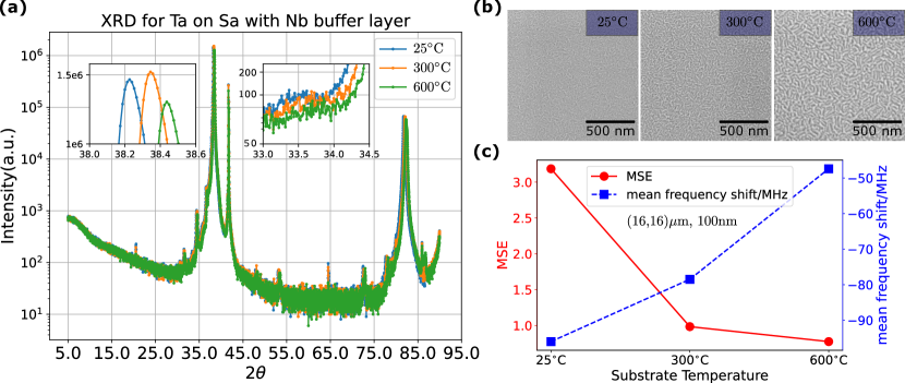
In addition to Ta film thickness, the substrate temperature during Ta sputtering is another crucial factor affecting and . In general, higher temperatures lead to larger grain sizes and consequently fewer grain boundaries [18], resulting in a structure that more closely resembles the bulk superconductor, characterized by a smaller . However, altering the temperature of the sapphire substrate changes the lattice matching conditions between sapphire and Ta, leading to different Ta film phases and other phases may have larger loss than [23, 24, 3, 4]. To maintain the purity of the -phase, we introduce a 5 nm Nb buffer layer to ensure good lattice matching across different temperatures [21]. As shown in Fig. 3(a), we employ X-ray diffraction (XRD) to analyze the purity of -Ta. In the upper right inset, the primary peak remains nearly constant at various temperatures. The slight differences in diffraction arise from minor distortions in the -Ta lattice [25]. In the upper middle inset, we also do not observe -Ta, which locates at 33.7∘. In Fig. 3(b), we utilize scanning electron microscopy (SEM) to confirm the grain size change with different substrate temperatures. It is evident that a higher temperature leads to larger grain sizes.
We fabricate the test chip using the same design, only varying the substrate temperature during sputtering. The low-temperature results are summarized in Fig. 3(c). As the temperature increases to 600∘C, MSE decreases by more than three times. Additionally, is reduced by approximately 50 MHz. These findings suggest that a higher temperature will both reduce and enhance the resonator frequency stability against film thickness variations.
II.4 Geometry Optimization
In prior studies, the width of the center electrode and the gap between the center electrode and the ground electrode were kept at 16m. However, such wide SCPW resonators may not fit into the limited space available on large-scale superconducting quantum processors. Therefore, it is essential to optimize a set of SCPW resonator dimensions () to achieve low kinetic inductance within a fixed space constraint, such as m.
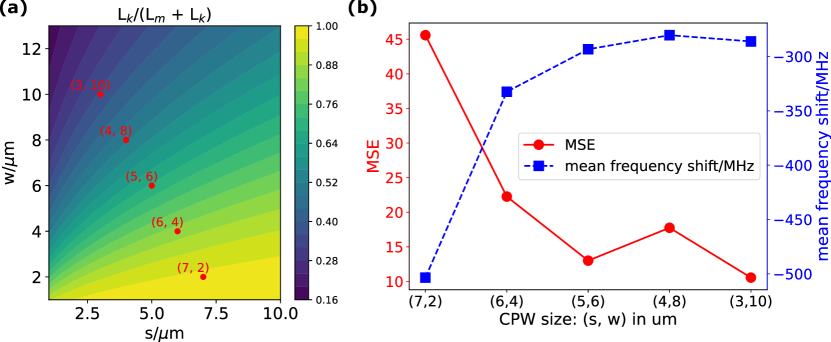
We calculate the kinetic inductance ratio to the total inductance using Eqn. 1 and in Ref. [10, 26, 11] with varying electrode width and the gap between the center electrode and ground electrode , as shown in Fig. 4(a). It is clear qualitatively that smaller and larger result in a smaller kinetic inductance ratio, which is preferred. We should keep in mind that the quantitative values in Fig. 4(a) may be inaccurate, because the formula we use is valid only when , but this may not hold true in our chip.
We maintain the total size of the SCPW resonator at 16 m and choose a series of () values. We ensure the mean resonator frequencies are always 6.7 GHz. The low-temperature results of MSE and are displayed in Fig. 4(b). As decreases from 7 m to 3 m, the MSE drops from about 45 to approximately 10, and the absolute decreases by 200 MHz. These findings indicate that a smaller gap and larger center width can effectively reduce and improve the resonator frequency stability against film thickness variations. Moreover, it is also suggested that when designing Purcell filters and resonators, it is preferable to maintain the same () values to minimize frequency mismatching caused by the difference in .
II.5 High Internal Quality Factor of the Optimized Resonator
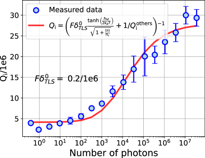
In superconducting quantum computing applications, we utilize a (16,16) m SCPW resonator with a 300 nm thickness, sputtered at 500∘C. The internal quality factor, , of this resonator has an empirical relationship with the qubit relaxation time () at 5 GHz. In our routine tests, we have observed that when the of this resonator (6.7 GHz) reaches , the highest of a single qubit fabricated with the same film can achieve s (5 GHz) in our lab. The of the SCPW resonator is measured at different microwave power levels, as shown in Fig. 5. Error bars represent ±1 standard deviation while fitting the of the resonator. The microwave flux photon number is calculated from the incident microwave power, the fitted coupling quality factor (about 0.7 million), the resonator frequency (6636 MHz), and the calculated impedance of the readout waveguide and the resonator [20]. At single photon power, the is approximately 2.5 million, which is similar to the best reported results on sapphire without a Nb buffer layer [27]. With this fabrication technique, according to the experience in our lab, we predict a best of qubit to be 250 s at 5 GHz. We fit the of the resonator measurements using the formula:
| (3) |
resulting in a filling factor-loss angle product , which is one of the lowest result for the 16 m gap [20], providing evidence for the suitability of our technology for high-coherence superconducting quantum chips.
III Discussion
Our study introduces a comprehensive method to minimize kinetic inductance in Ta-based SCPW resonators, effectively addressing frequency crowding issues. By carefully controlling Ta film thickness and substrate temperature during sputtering, and optimizing SCPW geometry, we achieved a significant reduction in uncontrolled frequency shifts and a 100-fold reduction in frequency variance characterized by MSE, crucial for the precision needed in multi-qubit systems. The high internal quality factor of 2.5 million at the single-photon power level, combined with the reduced kinetic inductance, highlights the potential of our approach for high-coherence, large-scale superconducting quantum chips.
These findings not only present a comprehensive strategy for optimizing Ta-based superconducting circuits but also provide insights into the impact of microstructure on superconducting properties, thereby laying the foundation for further enhancements in quantum device performance. By reversing the kinetic inductance reduction optimization methods detailed here, our work can be directly applied to nonlinear quantum devices that require large kinetic inductance, such as microwave kinetic inductance detectors [28] and kinetic inductance traveling wave parametric amplifiers [29].
IV Method
IV.1 Fabrication
To maintain high-purity -Ta under various sputtering conditions, especially at different temperatures, all Ta films are fabricated with an Nb buffer layer. First, a thin Nb buffer layer is deposited on a sapphire substrate using dc magnetron sputtering at room temperature. Second, Ta films with the desired thickness and temperature conditions are deposited using the same sputtering system. Next, we use ultraviolet exposure to define the resonators on the chip using a photoresist. After a brief development, an inductively coupled plasma (ICP) system is employed to remove unwanted Ta films. The wafer then undergoes ultrasonication with acetone and isopropanol for five minutes each. Additionally, the wafer is cleaned in a piranha solution to eliminate residual resist. Finally, the sample is diced into chips, and the protective resist is removed using a remover at 80∘C for over 12 hours.
IV.2 Low Temperature Measurement
All resonator measurements are conducted at approximately 13 mK in the mixing chamber (MXC) of a cryostat. The input attenuation for the chip includes 20 dB on the 3K layer, 3 dB on the still layer, 6 dB on the cold plate, and 40 dB on the MXC [30]. The output signal passes through two double junction isolators, a 40 dB gain High Electron Mobility Transistor (HEMT) at the 4K layer, and a final 40 dB gain room temperature amplifier. The measurements are performed using a Vector Network Analyzer (VNA) with a bandwidth precision of up to 1 Hz, and the bandwidth and repetitions are adjusted based on the criterion that the relative deviation of should be less than 20%. Two infrared (IR) filters are connected to both the input and output ports of the chip, which is packaged in a 4-port aluminum box and thermally attached to the mixing chamber.
The rescaled is fitted using the formula [31]: , where represents the complex coupled quality factor. The photon number reaching the resonator is calculated based on the power arriving at the chip and the external coupling quality factor , which is also determined from the fitting of experimental data [20]. To calculate the power reaching the chip, the input power from the VNA, in addition to the attenuators mentioned earlier, is reduced by an additional 10 dB to account for cable loss, which is independently calibrated.
References
- [1] De Leon, N. P. et al. Materials challenges and opportunities for quantum computing hardware. Science 372, eabb2823 (2021).
- [2] Murray, C. E. Material matters in superconducting qubits. Materials Science and Engineering: R: Reports 146, 100646 (2021).
- [3] Place, A. P. et al. New material platform for superconducting transmon qubits with coherence times exceeding 0.3 milliseconds. Nature communications 12, 1779 (2021).
- [4] Wang, C. et al. Towards practical quantum computers: Transmon qubit with a lifetime approaching 0.5 milliseconds. npj Quantum Information 8, 3 (2022).
- [5] Bal, M. et al. Systematic improvements in transmon qubit coherence enabled by niobium surface encapsulation. arXiv preprint arXiv:2304.13257 (2023).
- [6] Simmonds, R. W. et al. Decoherence in josephson phase qubits from junction resonators. Physical Review Letters 93, 077003 (2004).
- [7] Müller, C., Cole, J. H. & Lisenfeld, J. Towards understanding two-level-systems in amorphous solids: insights from quantum circuits. Reports on Progress in Physics 82, 124501 (2019).
- [8] Gubin, A., Il’in, K., Vitusevich, S., Siegel, M. & Klein, N. Dependence of magnetic penetration depth on the thickness of superconducting nb thin films. Physical Review B 72, 064503 (2005).
- [9] Yu, L. et al. Fabrication of niobium titanium nitride thin films with high superconducting transition temperatures and short penetration lengths. IEEE transactions on applied superconductivity 15, 44–48 (2005).
- [10] Watanabe, K., Yoshida, K. & Kohjiro, T. A. Kinetic inductance of superconducting coplanar waveguides. Japanese journal of applied physics 33, 5708 (1994).
- [11] Gao, J. The physics of superconducting microwave resonators (California Institute of Technology, 2008).
- [12] Blais, A., Grimsmo, A. L., Girvin, S. M. & Wallraff, A. Circuit quantum electrodynamics. Reviews of Modern Physics 93, 025005 (2021).
- [13] Li, Y., Wang, T., Hu, J., Li, D. & An, S. Optimizing resonator frequency stability in flip-chip architectures: A novel experimental design approach. arXiv preprint arXiv:2312.06405 (2023).
- [14] Doyle, S., Mauskopf, P., Naylon, J., Porch, A. & Duncombe, C. Lumped element kinetic inductance detectors. Journal of Low Temperature Physics 151, 530–536 (2008).
- [15] Kittel, C. & McEuen, P. Introduction to solid state physics (John Wiley & Sons, 2018).
- [16] López-Núñez, D. et al. Magnetic penetration depth of aluminum thin films. arXiv preprint arXiv:2311.14119 (2023).
- [17] Hylton, T. & Beasley, M. Effect of grain boundaries on magnetic field penetration in polycrystalline superconductors. Physical Review B 39, 9042 (1989).
- [18] Jones, S. G. et al. Grain size in low loss superconducting ta thin films on c axis sapphire. Journal of Applied Physics 134 (2023).
- [19] Krupka, J., Derzakowski, K., Tobar, M., Hartnett, J. & Geyer, R. G. Complex permittivity of some ultralow loss dielectric crystals at cryogenic temperatures. Measurement Science and Technology 10, 387 (1999).
- [20] McRae, C. R. H. et al. Materials loss measurements using superconducting microwave resonators. Review of Scientific Instruments 91 (2020).
- [21] Alegria, L. D. et al. Two-level systems in nucleated and non-nucleated epitaxial alpha-tantalum films. Applied Physics Letters 123 (2023).
- [22] Greytak, T. & Wernick, J. The penetration depth in several hard superconductors. Journal of Physics and Chemistry of Solids 25, 535–542 (1964).
- [23] Shiojiri, M., Shinkai, S., Sasaki, K., Yanagisawa, H. & Abe, Y. Preparation of low-resistivity -ta thin films on (001) si by conventional dc magnetron sputtering. Japanese journal of applied physics 42, 4499 (2003).
- [24] Wu, Y., Ding, Z., Xiong, K. & Feng, J. High-quality superconducting -ta film sputtered on the heated silicon substrate. Scientific Reports 13, 12810 (2023).
- [25] Colin, J. J., Abadias, G., Michel, A. & Jaouen, C. On the origin of the metastable -ta phase stabilization in tantalum sputtered thin films. Acta Materialia 126, 481–493 (2017).
- [26] Gao, J., Zmuidzinas, J., Mazin, B., Day, P. & Leduc, H. Experimental study of the kinetic inductance fraction of superconducting coplanar waveguide. Nuclear Instruments and Methods in Physics Research Section A: Accelerators, Spectrometers, Detectors and Associated Equipment 559, 585–587 (2006).
- [27] Crowley, K. D. et al. Disentangling losses in tantalum superconducting circuits. Physical Review X 13, 041005 (2023).
- [28] Day, P. K., LeDuc, H. G., Mazin, B. A., Vayonakis, A. & Zmuidzinas, J. A broadband superconducting detector suitable for use in large arrays. Nature 425, 817–821 (2003).
- [29] Klimovich, N. S. Traveling wave parametric amplifiers and other nonlinear kinetic inductance devices (California Institute of Technology, 2022).
- [30] Krinner, S. et al. Engineering cryogenic setups for 100-qubit scale superconducting circuit systems. EPJ Quantum Technology 6, 2 (2019).
- [31] Khalil, M. S., Stoutimore, M., Wellstood, F. & Osborn, K. An analysis method for asymmetric resonator transmission applied to superconducting devices. Journal of Applied Physics 111 (2012).
V Data and Code availability
All data needed to evaluate the conclusions in the paper are present in the paper or the supplementary materials. Codes used in the theoretical calculation are available from the corresponding author on reasonable request.
VI Author contributions
S.M.A. and D.F.L. planned the experiment and designed the chip. D.F.L., J.J.H., and Y.L. fabricated the device and performed room temperature measurements. D.F.L. and S.M.A. conducted low temperature measurements and analyzed the data. All authors contributed to the manuscript, which was composed by S.M.A. and D.F.L.
VII Competing Interests Statement.
The authors declare no competing interests.