Performance of Superconducting Resonators Suspended on SiN Membranes
Abstract
Correlated errors in superconducting circuits due to nonequilibrium quasiparticles are a notable concern in efforts to achieve fault tolerant quantum computing. The propagation of quasiparticles causing these correlated errors can potentially be mediated by phonons in the substrate. Therefore, methods that decouple devices from the substrate are possible solutions, such as isolating devices atop SiN membranes. In this work, we validate the compatibility of SiN membrane technology with high quality superconducting circuits, adding the technique to the community’s fabrication toolbox. We do so by fabricating superconducting coplanar waveguide resonators entirely atop a thin (110 nm) SiN layer, where the bulk Si originally supporting it has been etched away, achieving a suspended membrane where the shortest length to its thickness yields an aspect ratio of approximately . We compare these membrane resonators to on-substrate resonators on the same chip, finding similar internal quality factors at single photon levels. Furthermore, we confirm that these membranes do not adversely affect the resonator thermalization rate. With these important benchmarks validated, this technique can be extended to qubits.
The superconducting circuits architecture of quantum computing has made significant strides over the past decades, and much progress in coherence times has been credited to innovative fabrication developments [1, 2]. The field continues to advance towards fault tolerant computing with error correction [3, 4], and quantum advantage has been experimentally demonstrated [5, 6]. However, correlated qubit errors induced by quasiparticles remain a concern, as they cannot be addressed by standard error correction protocols [7, 8, 9]. These correlated errors may originate from high-energy impact events that generate quasiparticles, which spread throughout the chip possibly mediated by phonons in the bulk substrate [10, 11, 12]. Although quasiparticle tunneling no longer limits most qubit coherence times [13, 14, 15], unlike as some earlier work encountered [16, 17], quasiparticle-induced correlated errors must still be addressed with the ongoing pursuit toward error correction, while recognizing that quasiparticles may eventually become a limiting error source again. While efforts have been made to mitigate the impact of quasiparticles by reducing the energy of propagating phonons, using quasiparticle traps, and gap engineering of the qubit’s junction [18, 19, 20, 21, 22, 23], we explore an alternative approach.
Thin silicon nitride (SiN) membranes have found use in many different applications. Such membranes can be high-Q mechanical resonators [24, 25]. However, more relevant for this application of interest, they can partially isolate a device atop the membrane from the rest of the substrate. This isolation can achieve different goals - it can increase a device’s sensitivity to events of interest occurring at the membrane [26, 27], while it can also limit interaction with events occurring in the bulk substrate over which it spans [28, 29]. These membranes have demonstrated promise in reducing correlated events in microwave kinetic inductance detector (MKID) arrays composed of coplanar waveguide (CPW) resonators [30, 31, 32], where a portion of the CPW was suspended [29]. In these MKID arrays, quasiparticle impacts are detected by resonator frequency shifts, bearing similarities to superconducting circuit readout schemes [33, 34]. Thus, with such promising results and parallels between the systems, it is natural to probe the compatibility of SiN membranes and superconducting circuits.
In this work, we adapt this technique of suspending devices on thin SiN membranes to superconducting circuits. In contrast to works that have suspended Josephson junctions above the Si substrate by etching from the topside [35, 36], we suspend a device on a SiN layer and remove all bulk Si beneath it. Superconducting circuits require a low-loss environment to achieve high coherence times, so verifying that SiN membranes can yield such an environment is a crucial first step in their implementation. We accomplish this using CPW resonators, as their internal quality factor () probes the material quality [37, 38]. Ultimately, we find sufficient quality factors to justify applying this technique to qubits in an effort that could limit quasiparticle-induced correlated errors.
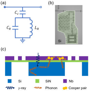
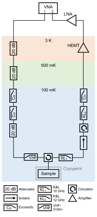
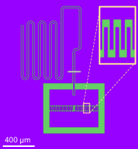
The CPW’s were patterned on 10 mm 10 mm Si chips, each consisting of eight resonators - four directly on the bulk substrate (on-substrate condition) and four on thin SiN membranes spanning the substrate (membrane condition). To the best of our knowledge, this is the first examination of a CPW fabricated entirely on a SiN membrane, offering insight into the quality factor and characteristics of such devices. All resonators were coupled to a central transmission line and measured in reflection, as shown in Fig. 1(a) and (b). A schematic illustration of the chip and the technique’s overarching goal of limiting correlated events from quasiparticles is shown in Fig. 1(c). Due to the membrane’s fragility, airbridges were necessary to galvanically stitch together the ground plane to reduce parasitic slotline modes, as opposed to using wirebonds [39, 40, 41]. We present the results from two samples principally characterized in an adiabatic demagnetization refrigerator (ADR) with a base temperature of 100 mK. A wiring diagram of this measurement setup is within Appendix A.
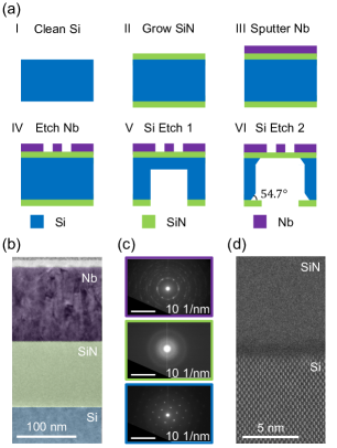
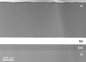
The device fabrication combined methods from superconducting circuits with those for fabricating SiN membranes, with the major steps illustrated in Fig. 2(a), and further details are presented in Appendix B. The CPW resonators were etched from a 125 nm thick Nb layer atop a 110 nm SiN layer, which was grown on a high-resistivity Si wafer. The SiN was deposited using low pressure chemical vapor deposition (LPCVD), and silicon-rich was chosen instead of due to its lower dielectric loss [42]. The thickness of each layer was measured using cross-sectional transmission electron microscopy (TEM), shown in Fig. 2(b). Further details on the materials characterization can be found in Appendix C. The fabrication posed various challenges due to the fragility of the membranes, especially at the dimensions in this work. The ratio between the shortest (longest) span of the etched region and the SiN membrane thickness is approximately (). Successfully fabricating such a high aspect ratio membrane is encouraging to further apply this technique to devices requiring membranes over large areas.
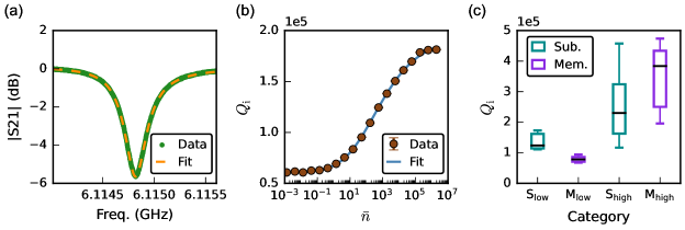
We used a variety of techniques to characterize the resonators in the frequency domain. The prime metric of interest is their internal quality factor, and to the best of our knowledge, we conducted the first measurements of the of CPW resonators on SiN membranes. , or its inverse the internal loss , was extracted by fitting the resonator’s scattering parameters to a reflection model, as shown in Fig. 3(a), using methods described in past work [38].
One significant loss source for resonators are two-level systems (TLS), whose effects are expected to saturate at high powers [43]. Thus, if TLS are a dominant loss source, is expected to increase with increasing power before saturating, and the difference between at low and high powers distinguishes the relative loss contribution from TLS versus other sources (note, in certain devices such as Al resonators at low temperature, can instead decrease with increasing drive power as more quasiparticles are generated [44]). The relevant values can be obtained by probing the resonator with a varying power to obtain versus average photon number (), which can be fit, as in Fig. 3(b), by
| (1) |
Here, is the low power TLS loss, is a filling factor, is a critical photon number, and is a power-independent loss term that will saturate to at high drive powers [38].
The on-substrate versus membrane resonators were compared by their low and high power values, as shown in Fig. 3(c), with the individual resonator plots shown in Appendix D. With reference to Eq. (1), the low power values correspond to , and the high power values correspond to . At low power, the membrane (on-substrate) resonators had a median of (); meanwhile, at high power, the membrane (on-substrate) resonators had a median of (). However, as seen in panel (c), the high power results were comparable to each other within their spreads.
One possible explanation of this difference at low power is a greater amount of TLS affecting the membrane resonators. Those resonator’s fields occupy both the Nb metal-air interface and the bottom SiN-air interface, in contrast to the on-substrate resonators that do not encounter the latter air interface but instead a typically cleaner SiN-Si interface [45, 46]. This SiN-Si interface was more closely examined to confirm its relatively low levels of oxides, as shown within Appendix C.
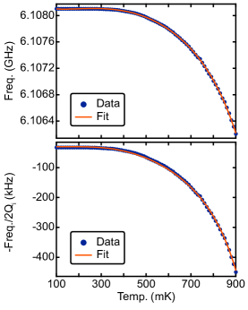
All resonators had aluminum (Al) airbridges spanning over the CPW signal trace. As the device temperature was increased closer to the superconducting transition temperature of Al () [47], we found systematic changes in the resonator frequency and that can be well fit using a cavity-perturbation model based on the Mattis-Bardeen theory [48] (see Appendix E for details). This indicates that the temperature evolutions were mainly associated with the changing Al surface impedance, instead of factors such as fabrication processing.
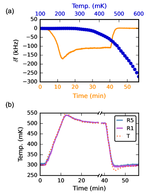
Leveraging this effect, we investigated whether the resonators on bulk substrate significantly differ in their thermalization rate compared to those on membrane. To do so, we first increased the cryostat’s temperature in 10 mK steps, and each resonator’s scattering parameters were measured using a VNA at high power (), chosen to ensure later scans could be taken quickly without averaging. From the resulting frequency versus temperature, as shown in blue in Fig. 4(a), we fit the relationship in the temperature regime of interest to a monotonic function, thus enabling the conversion between frequency and temperature. After these calibration measurements, the ADR’s base plate was swept up from 300 mK to 500 mK, held, and then swept back down. Throughout this process, the resonator response was monitored, with its fitted frequency shown in orange in Fig. 4(a). For each experiment, two resonators were monitored in an interleaved fashion to achieve a faster repetition rate. This experiment was repeated, where one resonator in the pair remained the same, while the other resonator changed. Although this did not allow for a comparison among all resonators from a single sweep, a thermalization difference between on-substrate versus membrane resonators would still be apparent in these pairwise sweeps.
Using the calibration scans to convert from frequency to temperature, we compared the temperatures versus time of each resonator in a pair, as in Fig. 4(b), where the thermometer reading of the cryostat is also displayed. For each of these experiments, we identified four time intervals where any thermalization differences between resonators should be more apparent. These correspond, in order, to when the ADR temperature initially increased from the low set point, when it maximized after reaching the high set point, when it initially began to decrease back to the low set point, and when it minimized after reaching the low set point again. If one resonator thermalized faster than the other, its temperature would change sooner in the first and third intervals, while it would achieve its maximum (minimum) temperature sooner in the second (fourth) interval. For all resonator pairs, no systematic difference in the thermalization rates was observed, with further details in Appendix F.
In this work, we successfully fabricated and characterized suspended CPW resonators on thin SiN membranes to evaluate whether high-Q superconducting circuits are compatible with such a technique. This exploration was motivated by the outstanding concern of mitigating correlated effects from quasiparticles on superconducting circuits. While previous experiments have suspended portions of CPW’s on SiN membranes [29, 27], this work is distinct in suspending the entire CPW on an extreme aspect ratio membrane and probing its and other properties, while incorporating materials common to superconducting circuits and fabricating high-Q resonators. Ultimately, we find such fabrication compatible with high-Q resonators, with the on-substrate resonators and membrane resonators having similar low power . These comparable values may suggest that suspending resonators does not limit their to the range. While these values remain below state-of-the-art levels for conventional on-substrate CPW’s [49, 38], more optimized cleaning, which could be further enabled by thicker membranes, or initially annealing the SiN [50] could yield improvements. Furthermore, one must note that this resonator quality factor doesn’t directly translate to a qubit quality factor on the same platform due to their different participation ratios [45, 51]. Indeed, qubits may exhibit greater quality factors compared to resonators of the same materials [52] or even to their constituent components [53].
Not only did we study the resonator values, but we also explored potential impacts of this membrane technique on thermalization rate, where no difference between resonator conditions was resolvable. These results may be surprising, as they suggest that resonator thermalization is primarily mediated by thin layers of SiN and Nb instead of the bulk substrate. Furthermore, we modelled the effect of the Al airbridges. Their impact on the resonator and frequency offers a temperature bound beyond which Al airbridges should no longer be used, with values decreasing to half their maximum at around mK. This property is important to keep in mind as efforts continue to explore operating superconducting circuits at higher temperatures [54, 55]. In addition to thermalization rate, we further explored whether the resonators conditions differed in their temporal frequency stability, finding no significant differences, with further details presented in Appendix G.
Ultimately, this work adds SiN membrane techniques to the superconducting circuit toolbox, demonstrating the compatibility of membranes with high-Q resonators that do not negatively affect device thermalization or temporal frequency stability. However, before applying this technique to qubit fabrication, one must verify that typical capacitance values can still be achieved, as this technique removes most of the relevant dielectric. Through simulations using Ansys HFSS, we found that typical capacitance values can still be attained, relying upon an IDC-like capacitor reminiscent of early designs [56]. A sufficient qubit-resonator coupling strength, , can also be achieved, with these simulations described in Appendix H. Having confirmed this, the potential of suspending qubits on SiN membranes to evaluate the effects on correlated errors from quasiparticles can be explored.
Acknowledgements
We thank Bingcheng Qing and Zahra Pedramrazi for assistance with cryogenic setups. We would also like to acknowledge the UC Berkeley Marvell Nanofabrication Laboratory, where sample fabrication was principally performed.
T.C. acknowledges support from the National Science Foundation Graduate Research Fellowship Program (NSF GRFP) under Grant No. DGE 1752814 and DGE 2146752. This material, including work performed at the Molecular Foundry, was funded in part by the U.S. Department of Energy, Office of Science, Office of Basic Energy Sciences, Materials Sciences and Engineering Division "High Coherence Multilayer Superconducting Structures for Large Scale Qubit Integration and Photonic Transduction program (QIS-LBNL)" and by the U.S. Department of Energy, Office of Science, Office of Advanced Scientific Computing Research Quantum Testbed Program under contract DE-AC02-05CH11231.
Appendices
Appendix A ADR Setup
Most characterization of devices was performed in an HPD Rainier 103 adiabatic demagnetization refrigerator (ADR) at a base temperature of 100 mK. The samples were measured in reflection using a central bus to interact with all resonators, minimizing the needed number of lines. A VNA was used for all measurements, and the ADR temperature could be reliably modified to perform temperature sweeps. Further details on the microwave setup are presented in Fig. 5, similar to past work where resonator characterization was performed [38].
Appendix B Fabrication Procedure
While the main fabrication steps were outlined in Fig. 2(a), we provide more extensive details here. To begin, a 6 inch, 675 m thick high-resistivity ( ohm-cm) Si wafer was cleaned using a piranha etch and a buffered-oxide etch (BOE). A 110 nm layer of Si-rich was then grown on both sides of the wafer [42]. Following this, 125 nm of Nb was sputtered on one side. A conventional optical lithography procedure was performed to write and develop the ground plane features. The Nb was then etched to yield these completed features, which were protected before moving on to write the etch windows on the opposite side of the wafer. Once developed, these windows were used to selectively etch through the SiN layer and Si wafer beneath the resonators using consecutive anisotropic, deep reactive ion etching (DRIE) following the Bosch process, with a target total etching depth of 600 m. Due to the fragility of the membranes but necessity of galvanically stitching together the ground plane, airbridges were written using a single-step grayscale process. After ion milling to ensure galvanic contact, Al was evaporated to yield the airbridges.
Liftoff following this evaporation was delayed due to the airbridge fragility; instead, the wafer topside was protected with a dedicated photoresist before etching the remaining Si with KOH, which self-terminates at the SiN layer. This overall two-part etch series of a dry then wet etch was challenging to optimize. Use of only KOH instead of starting with a dry etch was unsuccessful due to the etch spreading too wide while etching through the Si wafer, rendering it challenging to achieve target membrane dimensions. We found that beginning with the dry, anisotropic etch was necessary. Another component to optimize revolved around how KOH also etches Nb. Consequently, any exposed feature or side of the Nb layer would lead to a wafer-scale failure during the wet etch. Thus, in addition to the protective layer, a clamping tool was used to further isolate the wafer topside from KOH while etching.
With the membranes now formed but the wafer still whole, individual dies were cleaved by hand, following cleaving lines formed earlier. Using a dicing saw would be too vigorous and destroy the membranes. Once an individual die was obtained, liftoff was performed using room temperature acetone overnight, for around 12 hours. This differs from other liftoff techniques using hot (67∘C) acetone or hot (80∘C) or even room temperature Microposit Remover 1165, which were all too aggressive for the membranes [57]. Finally, the dies were transferred to IPA, where the solvent was removed using a critical point dryer (CPD). Again, removal of solvent by other means such as blow drying, spin drying, or a hot plate destroyed the membranes.
Appendix C Materials Characterization
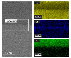
Materials characterization measurements were performed to examine the quality of the devices, similar to past work [38]. In preparation for TEM imaging, cross-section lamellae were prepared by FIB machining and extracted from the resonator chips. They were prepared at the Surface Analysis Laboratory, UTAH NANOFAB using a FEI Helios Nanolab 650 dual-beam at the University of Utah. Once the samples were received back to LBNL, TEM images and EDS elemental maps, such as that in Fig. 2 (b), were acquired at 200 kV using a JEOL 2100-F field emission scanning transmission electron microscope (STEM), which was equipped with an Oxford high-solid-angle silicon drift detector (SDD) x-ray energy dispersive spectrometer. For EDS spectral imaging, a 1-nm-diameter electron-beam probe was used. For finer resolution measurements, such as that in Fig. 2 (d), STEM-EELS was performed at 300 kV using the TEAM I double-aberration-corrected STEM equipped with a high-resolution Continuum Gatan imaging filter (GIF) spectrometer and a 4K 4K Gatan K3 direct electron detector. EELS spectral imaging maps were acquired using an electron-beam probe of a 0.1 nm diameter with 1-eV elastic-peak energy-resolution. A measurement of this chemical mapping is displayed in Fig. 6, showing the clean interface between the Si and SiN layers.
The resonator characterization is also notable in light of the Nb being grown on amorphous SiN, in contrast to the more standard case of growth on single crystalline Si. The Nb film on SiN exhibits a smaller grain size with random crystallographic orientation as compared to the larger grain sizes and preferred crystallographic orientation with apparent epitaxial Nb-grain nucleation observed in Nb on Si [38]. These distinctions raise further avenues of exploration concerning Nb growth on amorphous substrates and how the differences in grain size and orientation could affect its material properties and chemistry.
Appendix D Resonator Details
Here, we provide the measured values for each resonator of the two samples, measured at low power (single photon level) and high power, as shown in Fig. 7. Each chip had four resonators of each type on it. Although all resonators were found on Sample B, instead six were observed on Sample A.
Regarding the fitting routine of the resonator response versus power, in light of more noisy data at low power values, all fits were restricted to the interval above . Points were defined as outliers, likely due to noise at low powers or abnormal effects at high powers as also seen in other work [58, 59], and removed from the fitting procedure starting at if: (1) any low power point had a that decreased by more than relative to its neighboring next point, and (2) any high power point had a that increased by more than relative to its neighboring previous point.

Appendix E Airbridge Effect Modelling
The observed small relative change of frequency () with temperature () suggests that -dependent effects can be considered as perturbations to the resonant mode. In this cavity-perturbation regime [60], the evolution of the complex resonant frequency follows
| (2) |
where is a complex constant, is the surface impedance of the Al airbridges, is a real proportionality constant, and is the TLS contribution to the complex frequency shift. We ignore the surface impedance change of Nb because its is much higher than the range studied here.
We use the following expression for the TLS contribution [31, 43]:
| (3) |
where is the angular frequency, is the Boltzmann constant, and is the complex digamma function. Because the data were collected in the high-power regime where , here we have omitted the imaginary part of , which is suppressed by a factor of in comparison to its real part. We also set to the measured resonant frequency at 100 mK multiplied by , thanks to the minute relative change of .
For the airbridge contribution, as the penetration depth in Al is much smaller than the coherence length [61] and the airbridge thickness (615 nm as measured by TEM at the pads in contact with Nb, see Fig. 8), we calculate using
| (4) | |||
| (5) |
and according to the Mattis–Bardeen theory [48],
| (6) |
| (7) |
Here is the conductivity in the normal state, is the vacuum permeability, is the Fermi function at , and the superconducting gap is approximated as with representing the zero-temperature gap size. Eqs. (6) and (7) are valid for , which always holds in the temperature and frequency range of our measurements.
As shown in Fig. 9, we fit the real and imaginary parts of simultaneously using Eqs. (2)-(7). The independent fitting parameters are , , , , and . The integrals in Eqs. (6) and (7) are evaluated numerically using code modified from Ref. [62]. The fit well reproduces the overall temperature dependence, with mild overestimation of hardly visible on the plotted frequency scale. The surface impedance term is found to dominate the response, and the extracted and are in reasonable agreement with literature values for Al [61, 47]. These results indicate that the temperature-dependent effects can mainly be attributed to the Al airbridges.
Appendix F Thermalization Rate Comparison Analysis
Here, we present further information on the comparisons between resonator thermalization rates. For each region of interest, shaded in different colors in Fig. 10, the two resonator frequencies versus recorded point (earlier converted to temperature versus time in Fig. 4) were examined more closely to determine any significant differences. R1 and R4 are on SiN membranes, while R3, R5, and R6 are on-substrate.
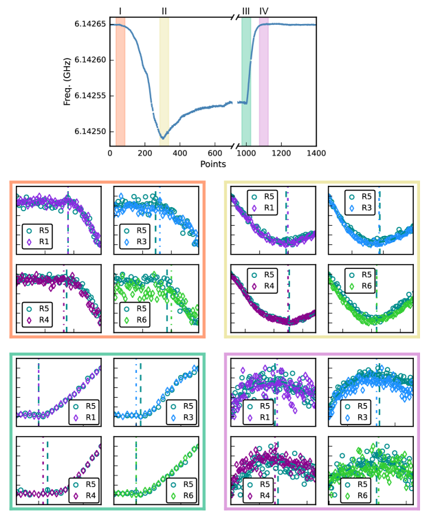
In region I (III), resonator thermalization differences would result in one resonator’s frequency changing sooner than the other. To identify the point when the resonator’s frequency started to change, with noise in mind, a moving average using a window of points was run across the data. The difference was taken between each window’s mean and the prior window’s, and the resonator’s initial point of change was identified as the point when all further window differences were negative (positive), meaning that the moving averages continually became lower (higher). In region II (IV), the resonator frequency versus point was fit to an asymmetric parabola, and the minimum (maximum) points were compared. The difference in these corresponding points for each pair of resonators is presented in Table 1.
| Res. Pair | Reg. I | Reg. II | Reg. III | Reg. IV |
|---|---|---|---|---|
| 1-5 | 0 | 1 | 0 | 3 |
| 3-5 | 3 | 0 | -1 | -3 |
| 4-5 | -2 | -1 | -1 | -3 |
| 6-5 | 3 | 0 | 0 | 3 |
Appendix G Frequency Stability
To explore any differences in the temporal frequency stability of the resonators, a single point from each was monitored over approximately 90 minutes using a VNA at . A single point was chosen instead of a full scan over the resonator to achieve a faster repetition rate. Using initial scans across all resonators, by fitting the resonator’s phase versus frequency in an interval close to resonance, a linear relationship can be extracted to convert between the two [63]. This linear relationship is formally expressed by the Barkhausen relationship, [64, 65].
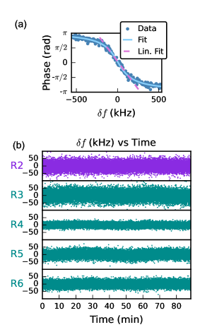
This calibration and measurement procedure was performed for on-substrate and membrane resonators on the same chip, as shown in Fig. 11. In contrast to results presented earlier, these measurements were performed in a dilution refrigerator at a temperature of 27 mK. To compare the resonator stability, we calculated the standard deviations () of the extracted frequency values over the duration of the scans [66], with results of each resonator presented in Table 2. Although certain resonators were more stable than others, no distinction was observed between membrane versus on-substrate resonators. Therefore, these results suggest that fabricating resonators on thin SiN membranes does not adversely affect their temporal frequency stability.
| Metric | R2 | R3 | R4 | R5 | R6 |
|---|---|---|---|---|---|
| (kHz) | 21 | 24 | 10 | 17 | 15 |
Appendix H HFSS Simulations
While the measured values of the membrane resonators confirm that high quality superconducting circuit devices are compatible with this membrane technique, designs for integrating qubits must be verified before applying this technique to them. While simulations related to designing the chips used in this work focused on resonator frequencies and external coupling values, a greater number of parameters must be verified when extending the technique to qubits. A main concern is balancing how the etching removes most of the dielectric while certain capacitance values must still be achieved.
To address this concern and verify the compatibility between qubits and these membranes, we conducted simulations using Ansys HFSS, a commonly used software for simulating superconducting circuit designs. We found that adding “fingers" to the qubit capacitor paddles yielded the desired capacitance ( fF); furthermore, moving the resonator coupling section closer to the qubit paddle and within the gap between it and the ground plane also yielded the desired qubit-resonator coupling ( MHz), both values typical of other transmon designs [67]. Both of these simulations were performed using the Eigenmode solver of HFSS. To identify the qubit capacitance, a lumped element inductor was placed between the capacitor paddles, modelled as 2D sheets with a perfect E boundary condition. From the simulated frequency of the associated mode, the corresponding capacitance was calculated. Meanwhile, was simulated by sweeping the inductance of the qubit mode through the resonator mode and scaling the avoided crossing difference back to the frequencies of interest. With these simulations as guidance, one can begin to explore placing qubits on SiN membranes.
References
- De Leon et al. [2021] N. P. De Leon, K. M. Itoh, D. Kim, K. K. Mehta, T. E. Northup, H. Paik, B. S. Palmer, N. Samarth, S. Sangtawesin, and D. W. Steuerman, Materials challenges and opportunities for quantum computing hardware, Science 372, 6539 (2021).
- Siddiqi [2021] I. Siddiqi, Engineering high-coherence superconducting qubits, Nat. Rev. Mater. 6, 875–891 (2021).
- Krinner et al. [2022] S. Krinner, N. Lacroix, A. Remm, A. Di Paolo, E. Genois, C. Leroux, C. Hellings, S. Lazar, F. Swiadek, J. Herrmann, G. J. Norris, C. K. Andersen, M. Müller, A. Blais, C. Eichler, and A. Wallraff, Realizing repeated quantum error correction in a distance-three surface code, Nature 605, 669–674 (2022).
- Google Quantum AI [2023] Google Quantum AI, Suppressing quantum errors by scaling a surface code logical qubit, Nature 614, 676–681 (2023).
- Arute et al. [2019] F. Arute, K. Arya, R. Babbush, D. Bacon, J. C. Bardin, R. Barends, R. Biswas, S. Boixo, F. G. S. L. Brandao, D. A. Buell, B. Burkett, Y. Chen, Z. Chen, B. Chiaro, R. Collins, W. Courtney, A. Dunsworth, E. Farhi, B. Foxen, A. Fowler, C. Gidney, M. Giustina, R. Graff, K. Guerin, S. Habegger, M. Harrigan, M. Hartmann, A. Ho, M. R. Hoffmann, T. Huang, T. Humble, S. Isakov, E. Jeffrey, Z. Jiang, D. Kafri, K. Kechedzhi, J. Kelly, P. Klimov, S. Knysh, A. Korotkov, F. Kostritsa, D. Landhuis, M. Lindmark, E. Lucero, D. Lyakh, S. Mandrà, J. R. McClean, M. McEwen, A. Megrant, X. Mi, K. Michielsen, M. Mohseni, J. Mutus, O. Naaman, M. Neeley, C. Neill, M. Y. Niu, E. Ostby, A. Petukhov, J. Platt, C. Quintana, E. G. Rieffel, P. Roushan, N. Rubin, D. Sank, K. J. Satzinger, V. Smelyanskiy, K. J. Sung, M. Trevithick, A. Vainsencher, B. Villalonga, T. White, Z. J. Yao, P. Yeh, A. Zalcman, H. Neven, and J. Martinis, Quantum supremacy using a programmable superconducting processor, Nature 574, 505–510 (2019).
- Wu et al. [2021] Y. Wu, W.-S. Bao, S. Cao, F. Chen, M.-C. Chen, X. Chen, T.-H. Chung, H. Deng, Y. Du, D. Fan, M. Gong, C. Guo, C. Guo, S. Guo, L. Han, L. Hong, H.-L. Huang, Y.-H. Huo, L. Li, N. Li, S. Li, Y. Li, F. Liang, C. Lin, J. Lin, H. Qian, D. Qiao, H. Rong, H. Su, L. Sun, L. Wang, S. Wang, D. Wu, Y. Xu, K. Yan, W. Yang, Y. Yang, Y. Ye, J. Yin, C. Ying, J. Yu, C. Zha, C. Zhang, H. Zhang, K. Zhang, Y. Zhang, H. Zhao, Y. Zhao, L. Zhou, Q. Zhu, C.-Y. Lu, C.-Z. Peng, X. Zhu, and J.-W. Pan, Strong quantum computational advantage using a superconducting quantum processor, Phys. Rev. Lett. 127, 180501 (2021).
- Fowler et al. [2012] A. G. Fowler, M. Mariantoni, J. M. Martinis, and A. N. Cleland, Surface codes: Towards practical large-scale quantum computation, Phys. Rev. A 86, 032324 (2012).
- Martinis [2021] J. M. Martinis, Saving superconducting quantum processors from decay and correlated errors generated by gamma and cosmic rays, npj Quantum Inf 7, 90 (2021).
- Wilen et al. [2021] C. D. Wilen, S. Abdullah, N. A. Kurinsky, C. Stanford, L. Cardani, G. D’Imperio, C. Tomei, L. Faoro, L. B. Ioffe, C. H. Liu, A. Opremcak, B. G. Christensen, J. L. DuBois, and R. McDermott, Correlated charge noise and relaxation errors in superconducting qubits, Nature 594, 369–373 (2021).
- Vepsäläinen et al. [2020] A. P. Vepsäläinen, A. H. Karamlou, J. L. Orrell, A. S. Dogra, B. Loer, F. Vasconcelos, D. K. Kim, A. J. Melville, B. M. Niedzielski, J. L. Yoder, S. Gustavsson, J. A. Formaggio, B. A. VanDevender, and W. D. Oliver, Impact of ionizing radiation on superconducting qubit coherence, Nature 584, 551–556 (2020).
- Cardani et al. [2021] L. Cardani, F. Valenti, N. Casali, G. Catelani, T. Charpentier, M. Clemenza, I. Colantoni, A. Cruciani, G. D’Imperio, L. Gironi, L. Grünhaupt, D. Gusenkova, F. Henriques, M. Lagoin, M. Martinez, G. Pettinari, C. Rusconi, O. Sander, C. Tomei, A. V. Ustinov, M. Weber, W. Wernsdorfer, M. Vignati, S. Pirro, and I. M. Pop, Reducing the impact of radioactivity on quantum circuits in a deep-underground facility, Nat Commun 12, 2733 (2021).
- McEwen et al. [2022] M. McEwen, L. Faoro, K. Arya, A. Dunsworth, T. Huang, S. Kim, B. Burkett, A. Fowler, F. Arute, J. C. Bardin, A. Bengtsson, A. Bilmes, B. B. Buckley, N. Bushnell, Z. Chen, R. Collins, S. Demura, A. R. Derk, C. Erickson, M. Giustina, S. D. Harrington, S. Hong, E. Jeffrey, J. Kelley, P. V. Klimov, F. Kostritsa, P. Laptev, A. Locharla, X. Mi, K. C. Miao, S. Montazeri, J. Mutus, O. Naaman, M. Neeley, C. Neill, A. Opremcak, C. Quintana, N. Redd, P. Roushan, D. Sank, K. J. Satzinger, V. Shvarts, T. White, Z. J. Yao, P. Yeh, J. Yoo, Y. Chen, V. Smelyanskiy, J. M. Martinis, H. Neven, A. Megrant, L. Ioffe, and R. Barends, Resolving catastrophic error bursts from cosmic rays in large arrays of superconducting qubits, Nat. Phys. 18, 107–111 (2022).
- Serniak et al. [2019] K. Serniak, S. Diamond, M. Hays, V. Fatemi, S. Shankar, L. Frunzio, R. J. Schoelkopf, and M. H. Devoret, Direct dispersive monitoring of charge parity in offset-charge-sensitive transmons, Phys. Rev. Applied 12, 014052 (2019).
- Kurter et al. [2022] C. Kurter, C. E. Murray, R. T. Gordon, B. B. Wymore, M. Sandberg, R. M. Shelby, A. Eddins, V. P. Adiga, A. D. K. Finck, E. Rivera, A. A. Stabile, B. Trimm, B. Wacaser, K. Balakrishnan, A. Pyzyna, J. Sleight, M. Steffen, and K. Rodbell, Quasiparticle tunneling as a probe of josephson junction barrier and capacitor material in superconducting qubits, npj Quantum Inf 8, 31 (2022).
- Pan et al. [2022] X. Pan, Y. Zhou, H. Yuan, L. Nie, W. Wei, L. Zhang, J. Li, S. Liu, Z. H. Jiang, G. Catelani, L. Hu, F. Yan, and D. Yu, Engineering superconducting qubits to reduce quasiparticles and charge noise, Nat Commun 13, 7196 (2022).
- Sun et al. [2012] L. Sun, L. DiCarlo, M. D. Reed, G. Catelani, L. S. Bishop, D. I. Schuster, B. R. Johnson, G. A. Yang, L. Frunzio, L. Glazman, M. H. Devoret, and R. J. Schoelkopf, Measurements of quasiparticle tunneling dynamics in a band-gap engineered transmon qubit, Phys. Rev. Lett. 108, 230509 (2012).
- Serniak et al. [2018] K. Serniak, M. Hays, G. de Lange, S. Diamond, S. Shankar, L. D. Burkhart, L. Frunzio, M. Houzet, and M. H. Devoret, Hot nonequilibrium quasiparticles in transmon qubits, Phys. Rev. Lett. 121, 157701 (2018).
- Riwar et al. [2016] R.-P. Riwar, A. Hosseinkhani, L. D. Burkhart, Y. Y. Gao, R. J. Schoelkopf, L. I. Glazman, and G. Catelani, Normal-metal quasiparticle traps for superconducting qubits, Phys. Rev. B 94, 104516 (2016).
- Patel et al. [2017] U. Patel, I. V. Pechenezhskiy, B. L. T. Plourde, M. G. Vavilov, and R. McDermott, Phonon-mediated quasiparticle poisoning of superconducting microwave resonators, Phys. Rev. B 96, 220501(R) (2017).
- Henriques et al. [2019] F. Henriques, F. Valenti, T. Charpentier, M. Lagoin, M. Vignati, L. Grünhaupt, D. Gusenkova, J. Ferrero, S. T. Skacel, W. Wernsdorfer, A. V. Ustinov, G. Catelani, O. Sander, and I. M. Pop, Phonon traps reduce the quasiparticle density in superconducting circuits, Appl. Phys. Lett. 115, 212601 (2019).
- Iaia et al. [2022] V. Iaia, J. Ku, A. Ballard, C. P. Larson, E. Yelton, C. H. Liu, S. Patel, R. McDermott, and B. L. T. Plourde, Phonon downconversion to suppress correlated errors in superconducting qubits, Nat. Commun. 13, 6425 (2022).
- Bargerbos et al. [2023] A. Bargerbos, L. J. Splitthoff, M. Pita-Vidal, J. J. Wesdorp, Y. Liu, P. Krogstrup, L. P. Kouwenhoven, C. K. Andersen, and L. Grünhaupt, Mitigation of quasiparticle loss in superconducting qubits by phonon scattering, Phys. Rev. Applied 19, 024014 (2023).
- McEwen et al. [2024] M. McEwen, K. C. Miao, J. Atalaya, A. Bilmes, A. Crook, J. Bovaird, J. M. Kreikebaum, N. Zobrist, E. Jeffrey, B. Ying, A. Bengtsson, H.-S. Chang, A. Dunsworth, J. Kelly, Y. Zhang, E. Forati, R. Acharya, J. Iveland, W. Liu, S. Kim, B. Burkett, A. Megrant, Y. Chen, C. Neill, D. Sank, M. Devoret, and A. Opremcak, Resisting high-energy impact events through gap engineering in superconducting qubit arrays, arXiv preprint arXiv:2402.15644 (2024).
- Zwickl et al. [2008] B. M. Zwickl, W. E. Shanks, A. M. Jayich, C. Yang, A. C. B. Jayich, J. D. Thompson, and J. G. E. Harris, High quality mechanical and optical properties of commerical silicon nitride membranes, Appl. Phys. Lett. 92, 103125 (2008).
- Yuan et al. [2015] M. Yuan, M. A. Cohen, and G. A. Steele, Silicon nitride membrane resonators at millikelvin temperatures with quality factors exceeding , Appl. Phys. Lett. 107, 263501 (2015).
- Fyhrie et al. [2016] A. Fyhrie, C. McKenney, J. Glenn, H. G. LeDuc, J. Gao, P. Day, and J. Zmuidzinas, Responsivity boosting in FIR TiN LEKIDs using phonon recycling: simulations and array design, SPIE Proceedings 9914, 10.1117/12.2231476 (2016).
- de Visser et al. [2021] P. J. de Visser, S. A. de Rooij, V. Murugesan, D. J. Thoen, and J. J. Baselmans, Phonon-trapping-enhanced energy resolution in superconducting single-photon detectors, Phys. Rev. Applied 16, 034051 (2021).
- Lindeman et al. [2014] M. A. Lindeman, J. A. Bonetti, B. Bumble, P. K. Day, B. H. Eom, W. A. Holmes, and A. W. Kleinsasser, Arrays of membrane isolated yttrium-barium-copper-oxide kinetic inductance bolometers, Appl. Phys. Lett. 115, 234509 (2014).
- Karatsu et al. [2019] K. Karatsu, A. Endo, J. Bueno, P. J. de Visser, R. Barends, D. J. Thoen, V. Murugesan, N. Tomita, and J. J. A. Baselmans, Mitigation of cosmic ray effect on microwave kinetic inductance detector arrays, Appl. Phys. Lett. 114, 032601 (2019).
- Day et al. [2003] P. K. Day, H. G. LeDuc, B. A. Mazin, A. Vayonakis, and J. Zmuidzinas, A broadband superconducting detector suitable for use in large arrays, Nature 425, 817–821 (2003).
- Gao [2008] J. Gao, The Physics of Superconducting Microwave Resonators, Ph.D. thesis, California Institute of Technology (2008).
- Mazin [2009] B. A. Mazin, Microwave kinetic inductance detectors: The first decade, AIP Conference Proceedings 1185, 135–142 (2009).
- Blais et al. [2004] A. Blais, R.-S. Huang, A. Wallraff, S. M. Girvin, and R. J. Schoelkopf, Cavity quantum electrodynamics for superconducting electrical circuits: An architecture for quantum computation, Phys. Rev. A 69, 062320 (2004).
- Wallraff et al. [2005] A. Wallraff, D. I. Schuster, A. Blais, L. Frunzio, J. Majer, M. H. Devoret, S. M. Girvin, and R. J. Schoelkopf, Approaching unit visibility for control of a superconducting qubit with dispersive readout, Phys. Rev. Lett. 95, 060501 (2005).
- Chu et al. [2016] Y. Chu, C. Axline, C. Wang, T. Brecht, Y. Y. Gao, L. Frunzio, and R. J. Schoelkopf, Suspending superconducting qubits by silicon micromachining, Appl. Phys. Lett. 109, 112601 (2016).
- Pechenezhskiy et al. [2020] I. V. Pechenezhskiy, R. A. Mencia, L. B. Nguyen, Y.-H. Lin, and V. E. Manucharyan, The superconducting quasicharge qubit, Nature 585, 368–371 (2020).
- McRae et al. [2020] C. R. H. McRae, H. Wang, J. Gao, M. R. Vissers, T. Brecht, A. Dunsworth, D. P. Pappas, and J. Mutus, Materials loss measurements using superconducting microwave resonators, Rev. Sci. Instrum. 91, 091101 (2020).
- Altoé et al. [2022] M. V. P. Altoé, A. Banerjee, C. Berk, A. Hajr, A. Schwartzberg, C. Song, M. Alghadeer, S. Aloni, M. J. Elowson, J. M. Kreikebaum, E. K. Wong, S. M. Griffin, S. Rao, A. Weber-Bargioni, A. M. Minor, D. I. Santiago, S. Cabrini, I. Siddiqi, and D. F. Ogletree, Localization and mitigation of loss in niobium superconducting circuits, PRX Quantum 3, 020312 (2022).
- Hornibrook et al. [2013] J. M. Hornibrook, E. E. Mitchell, and D. J. Reilly, Suppressing dissipative paths in superconducting coplanar waveguide resonators, IEEE Trans. Appl. Supercond. 23, 3 (2013).
- Chen et al. [2014] Z. Chen, A. Megrant, J. Kelly, R. Barends, J. Bochmann, Y. Chen, B. Chiaro, A. Dunsworth, E. Jeffrey, J. Y. Mutus, P. J. J. O’Malley, C. Neill, P. Roushan, D. Sank, A. Vainsencher, J. Wenner, T. C. White, A. N. Cleland, and J. M. Martinis, Fabrication and characterization of aluminum airbridges for superconducting microwave circuits, Appl. Phys. Lett. 104, 052602 (2014).
- Sun et al. [2022] Y. Sun, J. Ding, X. Xia, X. Wang, J. Xu, S. Song, D. Lan, J. Zhao, and Y. Yu, Fabrication of airbridges with gradient exposure, Appl. Phys. Lett. 121, 074001 (2022).
- Paik and Osborn [2010] H. Paik and K. D. Osborn, Reducing quantum-regime dielectric loss of silicon nitride for superconducting quantum circuits, Appl. Phys. Lett. 96, 072505 (2010).
- Pappas et al. [2011] D. P. Pappas, M. R. Vissers, D. S. Wisbey, J. S. Kline, and J. Gao, Two level system loss in superconducting microwave resonators, IEEE Trans. Appl. Supercond. 21, 871–874 (2011).
- de Visser et al. [2014] P. J. de Visser, D. J. Goldie, P. Diener, S. Withington, J. J. A. Baselmans, and T. M. Klapwijk, Evidence of a nonequilibrium distribution of quasiparticles in the microwave response of a superconducting aluminum resonator, Phys. Rev. Lett. 112, 047004 (2014).
- Wenner et al. [2011] J. Wenner, R. Barends, R. C. Bialczak, Y. Chen, J. Kelly, E. Lucero, M. Mariantoni, A. Megrant, P. J. J. O’Malley, D. Sank, A. Vainsencher, H. Wang, T. C. White, Y. Yin, J. Zhao, A. N. Cleland, and J. M. Martinis, Surface loss simulations of superconducting coplanar waveguide resonators, Appl. Phys. Lett. 99, 113513 (2011).
- Woods et al. [2019] W. Woods, G. Calusine, A. Melville, A. Sevi, E. Golden, D. K. Kim, D. Rosenberg, J. L. Yoder, and W. D. Oliver, Determining interface dielectric losses in superconducting coplanar-waveguide resonators, Phys. Rev. Applied 12, 014012 (2019).
- Caplan and Chanin [1965] S. Caplan and G. Chanin, Critical-field study of superconducting aluminum, Phys. Rev. 138, A1428 (1965).
- Mattis and Bardeen [1958] D. C. Mattis and J. Bardeen, Theory of the anomalous skin effect in normal and superconducting metals, Physical Review 111, 412 (1958).
- Megrant et al. [2012] A. Megrant, C. Neill, R. Barends, B. Chiaro, Y. Chen, L. Feigl, J. Kelly, E. Lucero, M. Mariantoni, P. J. J. O’Malley, D. Sank, A. Vainsencher, J. Wenner, T. C. White, Y. Yin, J. Zhao, C. J. Palmstrøm, J. M. Martinis, and A. N. Cleland, Planar superconducting resonators with internal quality factors above one million, Appl. Phys. Lett. 100, 113510 (2012).
- Mittal et al. [2023] S. Mittal, K. Adachi, N. E. Frattini, M. D. Urmey, S.-X. Lin, A. E. Emser, C. Metzger, L. Talamo, S. Dickson, D. Carlson, S. B. Papp, C. A. Regal, and K. W. Lehnert, Annealing reduces microwave-frequency dielectric loss in superconducting resonators, arXiv preprint arXiv:2312.13504 (2023).
- Wang et al. [2015] C. Wang, C. Axline, Y. Y. Gao, T. Brecht, Y. Chu, L. Frunzio, M. H. Devoret, and R. J. Schoelkopf, Surface participation and dielectric loss in superconducting qubits, Appl. Phys. Lett. 107, 162601 (2015).
- Murray [2021] C. E. Murray, Material matters in superconducting qubits, Mater. Sci. Eng. R Rep. 146, 100646 (2021).
- Mencia et al. [2024] R. A. Mencia, W.-J. Lin, H. Cho, M. G. Vavilov, and V. E. Manucharyan, Integer fluxonium qubit, arXiv preprint arXiv:2403.16780 (2024).
- Anferov et al. [2023] A. Anferov, K.-H. Lee, F. Zhao, J. Simon, and D. I. Schuster, Improved coherence in optically-defined niobium trilayer junction qubits, arXiv preprint arXiv:2306.05883 (2023).
- Anferov et al. [2024] A. Anferov, S. P. Harvey, F. Wan, J. Simon, and D. I. Schuster, Superconducting qubits above 20 GHz operating over 200 mK, arXiv preprint arXiv:2402.03031 (2024).
- Koch et al. [2007] J. Koch, T. M. Yu, J. Gambetta, A. A. Houck, D. I. Schuster, J. Majer, A. Blais, M. H. Devoret, S. M. Girvin, and R. J. Schoelkopf, Charge-insensitive qubit design derived from the cooper pair box, Phys. Rev. A 76, 042319 (2007).
- Kreikebaum et al. [2020] J. M. Kreikebaum, K. P. O’Brien, A. Morvan, and I. Siddiqi, Improving wafer-scale josephson junction resistance variation in superconducting quantum coherent circuits, Supercond. Sci. Technol. 33, 06LT02 (2020).
- Crowley et al. [2023] K. D. Crowley, R. A. McLellan, A. Dutta, N. Shumiya, A. P. Place, X. H. Le, Y. Gang, T. Madhavan, M. P. Bland, R. Chang, N. Khedkar, Y. C. Feng, E. A. Umbarkar, X. Gui, L. V. Rodgers, Y. Jia, M. M. Feldman, S. A. Lyon, M. Liu, R. J. Cava, A. A. Houck, and N. P. de Leon, Disentangling losses in tantalum superconducting circuits, Phys. Rev. X 13, 041005 (2023).
- Drimmer et al. [2024] M. Drimmer, S. Telkamp, F. L. Fischer, I. C. Rodrigues, C. Todt, F. Krizek, D. Kriegner, C. Müller, W. Wegscheider, and Y. Chu, The effect of niobium thin film structure on losses in superconducting circuits, arXiv preprint arXiv:2403.12164 (2024).
- Klein et al. [1993] O. Klein, S. Donovan, M. Dressel, and G. Grüner, Microwave cavity perturbation technique: Part I: Principles, Int. J. of Infrared and Millim. Waves 14, 2423 (1993).
- Miller [1960] P. B. Miller, Surface impedance of superconductors, Physical Review 118, 928 (1960).
- Aude [2010] D. P. L. Aude, Modeling superconductors using surface impedance techniques, Bachelor’s thesis, Massachusetts Institute of Technology (2010).
- Grünhaupt et al. [2018] L. Grünhaupt, N. Maleeva, S. T. Skacel, M. Calvo, F. Levy-Bertrand, A. V. Ustinov, H. Rotzinger, A. Monfardini, G. Catelani, and I. M. Pop, Loss mechanisms and quasiparticle dynamics in superconducting microwave resonators made of thin-film granular aluminum, Phys. Rev. Lett. 121, 117001 (2018).
- Rubiola [2010] E. Rubiola, Phase Noise and Frequency Stability in Oscillators (Cambridge University Press, 2010).
- Niepce [2020] D. Niepce, Superinductance and Fluctuating Two-Level Systems: Loss and Noise in Disordered and Non-Disordered Superconducting Quantum Devices, Ph.D. thesis, Chalmers University of Technology (2020).
- Niepce et al. [2021] D. Niepce, J. J. Burnett, M. Kudra, J. H. Cole, and J. Bylander, Stability of superconducting resonators: Motional narrowing and the role of Landau-Zener driving of two-level defects, Science Advances 7, 39 (2021).
- Nguyen et al. [2023] L. B. Nguyen, N. Goss, K. Siva, Y. Kim, E. Younis, B. Qing, A. Hashim, D. I. Santiago, and I. Siddiqi, Empowering high-dimensional quantum computing by traversing the dual bosonic ladder, arXiv preprint arXiv:2312.17741 (2023).