Characterization of Silicon Photomultiplier Photon Detection Efficiency at Liquid Nitrogen Temperature
Abstract
The detection of individual photons at cryogenic temperatures is of interest to many experiments searching for physics beyond the Standard Model. Silicon photomultipliers are often deployed in liquid argon or liquid xenon to detect scintillation light by either directly detecting the vacuum ultra-violet scintillation or by detecting light from fluorescent compounds that are used to shift the wavelength. Here we present results from an experimental setup that measures the photon detection efficiencies of silicon photomultipliers, sensitive to the visible spectrum, at liquid nitrogen temperature, 77 K. Results from a KETEK PM3325-WB-D0 and a Hamamatsu S13360-3050CS silicon photomultiplier exhibit a decrease in photon detection efficiency greater than 20% at liquid nitrogen temperature relative to room temperature for nm light.
1 Introduction
A silicon photomultiplier (SiPM) is a solid-state detector with single-photon resolution and can be used to determine the arrival time of individual photons with nanosecond precision. This makes SiPMs ideal candidates for low-light detection applications [1]. A SiPM contains an array of Single Photon Avalanche Diodes (SPADs), each containing a quenching RC circuit, and is operated a few volts above the breakdown voltage. An incident photon can be absorbed within a SPAD and trigger a self-sustaining avalanche of charge carriers with some probability. Several rare-event search experiments have operated SiPMs at cryogenic temperatures [2, 3], or are planning on operating at cryogenic temperatures to detect the scintillation light from liquid argon and liquid xenon [4, 5, 6].
The work here is motivated by LEGEND — an experiment searching for neutrinoless double-beta () decay in 76Ge — because it uses SiPMs for the readout of its liquid argon (LAr) scintillation detector [7, 8]. The detection of argon scintillation in coincidence with a germanium detector energy deposition is used to tag and remove events that do not resemble decay, which should be contained entirely within the germanium. The liquid argon scintillation, peaked at 128 nm in the vacuum ultraviolet (VUV), is wavelength-shifted and guided to several arrays of SiPMs by a shroud of tetraphenyl butadiene (TPB) coated, wavelength-shifting optical fibers [9]. This method of collecting the VUV scintillation offers a large area of exposure to scintillation as opposed to using VUV-sensitive SiPMs; in addition, the wavelength-shifting also better matches the spectral response of commercially available visible-light sensitive SiPMs. However, the total collection efficiency of the liquid argon veto — without accounting for shadowing from the LEGEND geometry — is expected to be of the total number of VUV photons produced [10].
Characterizing the photon detection efficiency (PDE) of SiPMs at cryogenic temperatures is important for understanding the LAr scintillation detector response of LEGEND-200 — the current phase of LEGEND that is actively taking data. The PDE is the probability of a SiPM to detect a single incident photon and convert it into a useful signal. Knowledge of the PDE is critical for modeling and understanding the backgrounds observed in the experiment. These cryogenic SiPM characterizations will also inform the design of the future phase of LEGEND with 1000 kg of active isotope which aims to reach a discovery sensitivity for decay beyond years. Knowledge of the SiPMs’ PDE at liquid argon temperature (87 K) from experimental characterizations is important for optimizing LEGEND-1000’s LAr light readout, and for accurately projecting the background [8]. In this paper, we report a characterization of the cryogenic PDEs of a KETEK PM3325-WB-D0 SiPM and a Hamamatsu S13360-3050CS SiPM111LEGEND currently uses KETEK PM33100T SiPMs; the KETEK PM3325-WB-D0 was one of the latest available SiPM models from KETEK before the acquisition of SiPM assets by BROADCOM®. The Hamamatsu SiPM, in contrast, has a higher PDE at the peak emission wavelength of the wavelength-shifting fibers currently used in LEGEND. near liquid argon temperature to determine potential effects on the efficiency of the LEGEND liquid argon scintillation readout system. We find that the cryogenic PDEs at nm for these two devices exhibit a greater than 20% decrease from their room temperature PDE values across a broad range of overvoltages.
2 Experimental Method
A SiPM characterization test stand has been built at the University of Washington to measure the PDE and other properties, such as the dark count rate and breakdown voltage, at both room temperature and at cryogenic temperature. The PDE () of a SiPM can be broken down into three components [1],
| (2.1) |
is the quantum efficiency, is the avalanche triggering probability, and is effective fill factor. Each of these can depend on the wavelength () of incoming light; the temperature () of the SiPM; and/or the overvoltage (), which is the difference between the operating reverse bias and the breakdown voltage.
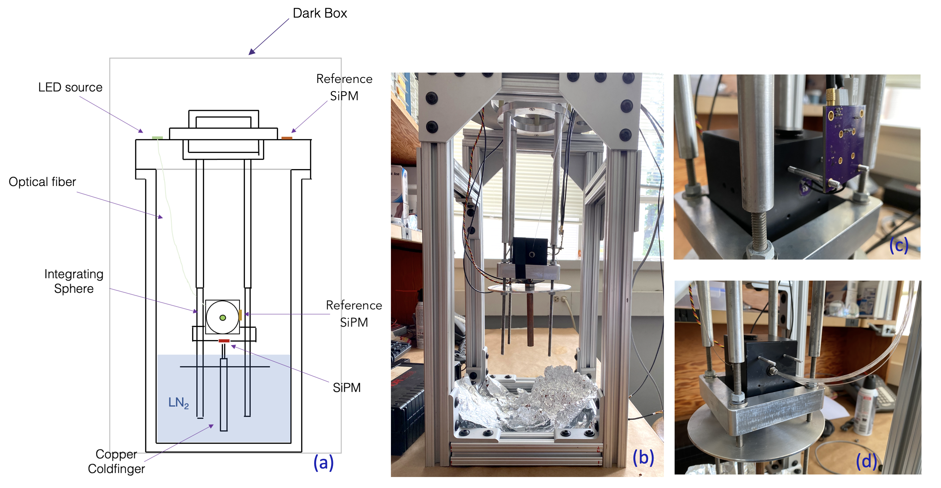
The setup consists of a ThorLabs IS200-4 integrating sphere suspended above a liquid nitrogen bath inside of a dewar contained inside a dark box as shown in Fig. 1. At each port of the integrating sphere, with perpendicular lines of sight, are the SiPM under test, a calibrated BROADCOM AFBR-S4K33C0135L SiPM (the reference SiPM), and a pulsed light emitting diode (LED) light source peaked at 562.5 nm with a full width at half maximum of 25 nm. One NanOpticsTM(030UC-00S) clear, double-cladded optical fiber connects the LED light source —located outside of the dewar — to the integrating sphere. The BROADCOM SiPM is used as a reference for the number of photons in the integrating sphere because its room temperature PDE is known absolutely. For room temperature PDE measurements, the reference diode is mounted directly to the integrating sphere; for cryogenic PDE measurements, the reference SiPM is placed at the lid of the dewar (thereby keeping it at room temperature) and is optically coupled to the integrating sphere by a bundle of the clear fibers. The SiPM signals are read out when triggered by an Agilent 33521 pulse generator that pulses the LED. The SiPM signals are pre-processed first with Texas Instruments LMH6629 transimpedance amplifiers near the integrating sphere and then with pre-amps consisting of two Analog Devices AD8014 amplifiers in series outside the dewar.
The absolute PDE () at liquid nitrogen temperature is calculated by taking the ratio of the number of detected photons at the SiPM () and the incoming flux of photons at the SiPM port () multiplied by the SiPM area (),
| (2.2) |
The incident flux on the test SiPM port is assumed to be equal to the incident flux on the reference SiPM port. During liquid nitrogen PDE measurements, the reference SiPM is placed at the lid of the dewar and is optically coupled to the integrating sphere by a bundle of the clear, double-cladded optical fibers, in order to preserve the known response () of the reference SiPM. Because the LED’s emission spectrum, , spans a range of wavelengths, the reference SiPM’s PDE should be a weighted average of the PDE across the LED’s emission spectrum,
| (2.3) |
is the spectral response of the reference SiPM; both and are available from the manufacturer. The reference SiPM is operated at a constant applied overvoltage of 5 V. The incident flux on the test SiPM is therefore expressed as
| (2.4) |
where is the number of photons detected by the reference SiPM during the liquid nitrogen temperature measurement, is the area of the reference SiPM, and is the flux ratio that corrects for the transmission coefficient to the reference SiPM (including, but not limited to, optical fiber transmission and coupling to the fibers) and any increased reflectivity in the sphere due to the fibers. The equality in Eqn. 2.4 assumes that light is distributed equally to both integrating sphere ports, that the transmission coefficient does not vary with temperature, and that the SiPMs are aligned perfectly normal to the port. The flux ratio can be measured by first comparing the number of photons measured by the reference SiPM at room temperature in this relative PDE configuration to the number of photons measured at room temperature when the reference SiPM is placed directly on the sphere. This is then normalized by the number of photons detected by the SiPM under test in order to correct for any fluctuations in the LED’s brightness or increased reflectivity from the fibers,
| (2.5) |
Here and are measured when both SiPMs are mounted directly on the integrating sphere, while and are measured with the test SiPM on the integrating sphere and the reference SiPM at the lid. These four quantities are measured at room temperature.
3 Data Acquisition and Processing
The signal output of the SiPMs were recorded by a CAEN DT5730 digitizer with a 500 MS/s sampling rate, 14-bit resolution, and dynamic range of 2 Vpp. The data were acquired using CAEN CoMPASS software [11]. The LED was pulsed with a 16 ns pulse width and a 1 kHz frequency from the function generator. Waveforms of length 10 s, with the trigger at s, were acquired to ensure the end of the waveform window would mimic dark conditions so that a dark count rate could be measured. Three sets of waveform data were taken with 90 s acquisition time at each overvoltage in order to improve statistics. This process of collecting waveform data at each overvoltage was done with the absolute PDE configuration at room temperature, and with the relative PDE configuration at room and liquid nitrogen temperatures. Further dark data were taken to enable a full characterization of the two SiPMs, see appendix A.
To ensure that the PDE measurements were not biased by correlated noise such as cross-talk, the pedestal method of measuring the PDE was used as described in [12]. To summarize, waveforms were acquired synchronously by triggering on the pulser so that baseline events, where the SiPM did not detect photons, were recorded. If the number of detected photons is Poisson distributed, then the probability of not detecting any photoelectrons, , gives an unbiased estimate of the Poissonian mean () because the baselines are unbiased by any correlated noise:
| (3.1) |
The probability of not detecting any photons is equal to the number of baseline events () divided by the total number of LED pulses (). In this way, the mean number of detected photons becomes
| (3.2) |
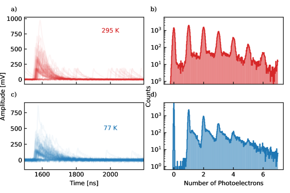
To get the number of baseline events the SiPM signals are first integrated in a 1 s window around the LED trigger time as well as the last 1 s of the waveform to get the dark count rate. Examples of the synchronously triggered waveforms are shown in Fig. 2a. When the histograms of these integrated signals are made, the peaks that correspond to the integral of the baseline events are called the pedestal peaks, as can be seen in Fig. 2b. The light level of the pulsed LED was set low enough so that an appreciable number of baseline events were acquired by making sure the pedestal peak was resolvable by eye when using the CoMPASS online energy spectrum. A Gaussian is then fit to the pedestal peaks in the histograms to determine the pedestal peak locations and standard deviations . The number of baseline events in light and dark conditions are then determined by the number of counts below a threshold. This routine is necessary because differences in the electronics noise between room and liquid nitrogen temperatures preclude the use of a single threshold. To get the mean number of photons detected by either the test SiPM or the reference SiPM () requires subtraction of the dark count rate,
| (3.3) |
is the number of baseline events in dark conditions, is the number of baseline events synchronous with the LED pulse. The total number of pulses is the same for both light and dark because the dark counts come from the portion of the waveform long after the LED turns off.
Post-processing of the data from CAEN CoMPASS is done with custom open source software, SiPM Studio222https://github.com/SamuelBorden/sipm_studio. This software parallel processes PDE data and automatically performs the Gaussian fits to the pedestal peak.
4 Results
The PDE was measured at room temperature and at liquid nitrogen temperature for the KETEK SiPM and Hamamatsu SiPM, see Fig. 3. Errors on all three quantities in Eq. 2.2 were propagated during error calculations. The room temperature was 72 ∘F (295 K) held by an air conditioning unit and the liquid nitrogen temperature was measured to be 77 K with a calibrated PT1000 sensor placed in between the SiPM board and copper cold finger. These temperatures were stable within 1 K during data taking. The breakdown voltage of the KETEK SiPM was measured at room temperature to be 24.1 V; the breakdown voltage at 77 K was 20.6 V. The breakdown voltages were obtained by extrapolating the SiPM gain, , as a function of reverse bias to and were confirmed with a reverse IV curve from a Keithley 2450 Sourcemeter®. Likewise, the breakdown voltage of the Hamamatsu SiPM was measured at room temperature to be 51.5 V; the breakdown voltage at 77 K was 42.2 V. Because the breakdown voltage depends on the temperature, the breakdown voltage was also used as a cross-check on the temperature. The breakdown voltages at liquid nitrogen temperature were determined by submerging the devices completely in liquid nitrogen in a separate experiment prior to the PDE measurement.

The PDE was measured for a range of overvoltages and results show a significant decrease in PDE at liquid nitrogen temperature for all overvoltages. This decrease in PDE is present even when accounting for possible changes in the optical properties of the setup at different temperatures or between configurations. Any systematic impact of the light uniformity in the integrating sphere or SiPM alignment would be seen during room temperature absolute PDE measurements. Our room temperature PDE measurements are in good agreement with the manufacturer’s datasheets, as seen in Fig. 3. Systematic studies were performed to determine if there was any temperature dependence in the transmission coefficient of the optical fibers connecting to the reference SiPM, the emission spectrum of the LED, or the reflectivity of the integrating sphere.
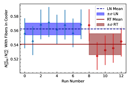
We characterized the temperature dependence of the optical fibers’ transmission coefficient (and the flux ratio ) by taking the dewar insert as shown in Fig. 1(d) and running cm of the cm long fibers through a Styrofoam cooler that was then filled with liquid nitrogen. The fibers were thus the only part of the test stand that was cold. One end of the fibers was connected to the integrating sphere, with the Hamamatsu SiPM placed at the opposite port, while the other end was coupled to the reference SiPM. The integrating sphere, the Hamamatsu SiPM, and the reference SiPM were all at room temperature. We then took PDE data with and without liquid nitrogen on the fibers while triggering on LED pulses sent into the integrating sphere. Fig. 4 shows the effective PDE — the number of photons detected by the Hamamatsu on the integrating sphere divided by the number of photons detected by the reference SiPM at the end of the fiber — when the fibers were at room and liquid nitrogen temperatures. The difference between the mean effective PDEs measured over several trials was found to be , which places a limit on the systematic error in our cryogenic PDE measurements.
We also investigated the systematics arising from the finite width of the LED’s emission spectrum. Using Eqn. 2.3 to calculate the reference SiPM PDE instead of using the reference SiPM’s PDE at the peak emission wavelength of the LED introduces only an average difference in our final cryogenic PDE results, which is below our statistical sensitivity. We therefore compute the cryogenic PDE using only the peak emission wavelength of the LED.
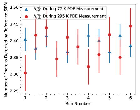
We checked that (the LED’s emission spectrum) and the integrating sphere’s optical properties were not functions of temperature. To do so, we compared the number of photons detected at the reference SiPM at 77 K and 295 K while the test stand was in the relative PDE measurement configuration. The reference SiPM has a comparable spectral response to the SiPMs under test. The results, shown in Fig. 5, indicate that the reference SiPM detects roughly the same number of photons when the test stand is at both room and cryogenic temperatures. Thus there is neither a shift in the emission spectrum of the LED nor a shift in the reflectivity of the integrating sphere. This measurement also serves as an in situ cross-check that the optical fibers’ transmission probability is not temperature dependent. Therefore, any changes in the optical properties of the test stand between the two temperatures do not account for the observed decrease in PDE.
The decrease in PDE at 77 K indicates that some combination of the quantum efficiency, avalanche triggering probability, and effective fill factor may be changing with temperature. Similar reductions of the PDE at cryogenic temperatures have been found in other SiPMs at 10 K using a calibrated system [13], and at 77 K using uncalibrated systems [14], [15] and calibrated systems [16]. Since silicon is an indirect band-gap semiconductor and fewer phonons are present in the crystal lattice at liquid nitrogen temperature, the probability of charge carriers moving to the conduction band from the absorption of a photon will be lower. This is reflected in the increase of the absorption depth of photons at a given energy at liquid nitrogen temperatures. The band-gap of silicon increases with decreasing temperature, but this may produce negligible effects on the quantum efficiency [17]. In addition, the recombination probability for electron-hole pairs before reaching the avalanche region may be higher at liquid nitrogen temperature. Similar findings were observed when researching the quantum efficiency of silicon thin film solar cells [18]. It is not expected that thermal expansion significantly impacts the effective fill factor because the thermal expansion coefficient for silicon at liquid nitrogen temperatures amounts to only a 0.02% change in area, which is too small to explain the observed decrease in PDE.
5 Conclusions
An experimental setup has been built at the University of Washington to characterize SiPMs at liquid nitrogen temperature to assess the efficiency of the liquid argon veto readout system to be deployed in LEGEND-1000. The SiPM test stand consists of an integrating sphere suspended above a liquid nitrogen bath in a dewar housed inside a dark box. The SiPM is in thermal contact with a copper cold finger that is partially submerged in liquid nitrogen and the integrating sphere is in a room-temperature thermal bath. Measurement of both a KETEK SiPM and Hamamatsu SiPM PDE at liquid nitrogen temperature suggests the liquid argon veto readout system has a lower efficiency compared to the expected PDE for room temperature operation. We expect the same behavior to persist at liquid argon temperatures because they are only K away from the measured liquid nitrogen temperatures: past studies have shown that the PDE at K for similar wavelengths is only times larger than the PDE at K [15]. The reduction in PDE seems to be caused by temperature dependencies to the intrinsic quantum efficiency and avalanche triggering probability of the SiPM. Changes to the effective fill factor may be present but are most likely negligible in comparison to the changes in quantum efficiency and avalanche triggering probability. The measurement of a decrease in PDE greater than 20% for all overvoltages at cryogenic temperatures for a SiPM sensitive to the visible spectrum is significant information for assessing and improving the background suppression capability of LEGEND-1000.
Acknowledgments
The authors appreciate the technical assistance and advice of J.F. Amsbaugh, T.H. Burritt, G. Giovanetti, G. Holman, A. Hostiuc, C.J. Nave, D. Peterson, G. Song, T.D. Van Wechel, I. Wang, and C. Wiseman.
References
- [1] F. Acerbi and S. Gundacker, Understanding and simulating SiPMs, Nuclear Instruments and Methods in Physics Research Section A: Accelerators, Spectrometers, Detectors and Associated Equipment 926 (2019) 16.
- [2] M. Chiappini, Meg ii physics and detector performance, Journal of Instrumentation 18 (2023) .
- [3] M. Agostini, A.M. Bakalyarov, M. Balata, I. Barabanov, L. Baudis, C. Bauer et al., Upgrade for phase ii of the gerda experiment, The European Physical Journal C 78 (2018) .
- [4] A. Jamil, T. Ziegler, P. Hufschmidt, G. Li, L. Lupin-Jimenez, T. Michel et al., Vuv-sensitive silicon photomultipliers for xenon scintillation light detection in nexo, IEEE Transactions on Nuclear Science 65 (2018) 2823–2833.
- [5] A. Falcone, A. Andreani, S. Bertolucci, C. Brizzolari, N. Buckanam, M. Capasso et al., Cryogenic sipm arrays for the dune photon detection system, Nuclear Instruments and Methods in Physics Research Section A: Accelerators, Spectrometers, Detectors and Associated Equipment 985 (2021) 164648.
- [6] C.E. Aalseth, F. Acerbi, P. Agnes, I.F. Albuquerque, T. Alexander, A. Alici et al., Darkside-20k: A 20 tonne two-phase lar tpc for direct dark matter detection at lngs, The European Physical Journal Plus 133 (2018) .
- [7] N. Abgrall, A. Abramov, N. Abrosimov, I. Abt, M. Agostini, M. Agartioglu et al., The large enriched germanium experiment for neutrinoless double beta decay (LEGEND), AIP Conference Proceedings 1894 (2017) 020027.
- [8] L. Collaboration, N. Abgrall, I. Abt, M. Agostini, A. Alexander, C. Andreoiu et al., LEGEND-1000 Preconceptual Design Report, arXiv:2107.11462 [nucl-ex, physics:physics] (2021) [2107.11462].
- [9] M. Schwarz, P. Krause, A. Leonhardt, L. Papp, S. Schöönert, C. Wiesinger et al., Liquid argon instrumentation and monitoring in legend-200, EPJ Web of Conferences 253 (2021) 11014.
- [10] M. Agostini, A. Alexander, G.R. Araujo, A.M. Bakalyarov, M. Balata, I. Barabanov et al., Liquid argon light collection and veto modeling in gerda phase ii, The European Physical Journal C 83 (2023) .
- [11] “Caen compass multiparametric daq software for physics applications.” https://www.caen.it/products/compass/.
- [12] A. Otte, J. Hose, R. Mirzoyan, A. Romaszkiewicz, M. Teshima and A. Thea, A measurement of the photon detection efficiency of silicon photomultipliers, Nuclear Instruments and Methods in Physics Research Section A: Accelerators, Spectrometers, Detectors and Associated Equipment 567 (2006) 360–363.
- [13] M. Ma, J. Zhou, F. Gu, J. Liao, Y. Gao, Z. Peng et al., Photo-detection efficiency measurement for fbk hd near-uv sensitive sipms at 10 k temperature, Dec, 2023.
- [14] F. Acerbi, G. Paternoster, S. Merzi, N. Zorzi and A. Gola, Nuv and vuv sensitive silicon photomultipliers technologies optimized for operation at cryogenic temperatures, Nuclear Instruments and Methods in Physics Research Section A: Accelerators, Spectrometers, Detectors and Associated Equipment 1046 (2023) 167683.
- [15] G. Collazuol, M.G. Bisogni, S. Marcatili, C. Piemonte and A. Del Guerra, Studies of silicon photomultipliers at cryogenic temperatures, Nuclear Instruments and Methods in Physics Research Section A: Accelerators, Spectrometers, Detectors and Associated Equipment 628 (2011) 389.
- [16] R. Álvarez-Garrote, E. Calvo, A. Canto, J.I. Crespo-Anadón, C. Cuesta, A.d.l.T. Rojo et al., Measurement of the photon detection efficiency of hamamatsu vuv4 sipms at cryogenic temperature, Apr, 2024.
- [17] W. Bludau, A. Onton and W. Heinke, Temperature dependence of the band gap of silicon, Journal of Applied Physics 45 (1974) 1846.
- [18] T. Wagner and U. Rau, Temperature-dependent quantum efficiency analysis of recombination centers in silicon thin-film solar cells, in Proceedings of 3rd World Conference onPhotovoltaic Energy Conversion, 2003, vol. 2, pp. 1162–1165 Vol.2, May, 2003, DOI.
- [19] A. Gola, F. Acerbi, M. Capasso, M. Marcante, A. Mazzi, G. Paternoster et al., Nuv-sensitive silicon photomultiplier technologies developed at fondazione bruno kessler, Sensors 19 (2019) 308.
- [20] F. Acerbi, A. Ferri, G. Zappala, G. Paternoster, A. Picciotto, A. Gola et al., Nuv silicon photomultipliers with high detection efficiency and reduced delayed correlated-noise, IEEE Transactions on Nuclear Science 62 (2015) 1318–1325.
- [21] I. Tobehn-Steinhäuser, M. Reiche, M. Schmelz, R. Stolz, T. Fröhlich and T. Ortlepp, Carrier mobility in semiconductors at very low temperatures, The 8th International Symposium on Sensor Science (2021) .
- [22] M. Guarise, M. Andreotti, R. Calabrese, A. Cotta Ramusino, V. Cicero, M. Fiorini et al., A newly observed phenomenon in the characterisation of sipm at cryogenic temperature, Journal of Instrumentation 16 (2021) .
Appendix A Dark Characterization
To estimate the SiPM dark count behavior, we took additional data under no LED illumination while the digitizer triggered on waveforms close to the 0.5 photoelectron amplitude. Waveforms with 10 s long traces were acquired for 60 seconds at each reverse bias at room temperature; however, at liquid nitrogen temperatures, an hour of data per reverse bias was taken to ensure high enough statistics. The custom software processed dark data by Wiener filtering the waveforms to get a more precise determination of dark pulses’ amplitude and arrival time. Wiener filtering allows for an unbiased estimate of pulse height even when a pulse occurs on the decay tail of a previous pulse.
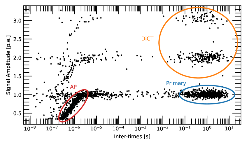
Under no illumination, SPADs can trigger an avalanche from thermal excitations due to the environment’s ambient temperature along with other correlated noise: direct cross-talk (DiCT), delayed cross-talk (DeCT), and afterpulsing (AP). The number of thermal excitations observed within a timing window is described by a Poisson distribution, thus the probability density function of inter-time spacings is an exponential distribution
| (A.1) |
where is the primary dark count rate. Secondary photons generated in an avalanche have some probability of triggering another avalanche in a neighboring SPAD simultaneously, which causes a waveform that is an integer multiple times larger than the single photoelectron signal, called direct cross-talk (DiCT). The DiCT probability is calculated as the ratio of events beyond the 1.5 photoelectron threshold to that beyond the 0.5 photoelectron threshold. It is also possible for the cross-talk to be delayed if the secondary photons create charge carriers that diffuse towards the avalanche region on the 10 ns time scale, called delayed cross-talk (DeCT). DeCT was not observed to be a significant contribution to dark counts from the KETEK SiPM or Hamamatsu SiPM. Afterpulsing (AP) is the probability a trapped charge carrier during an avalanche re-releases and triggers an additional avalanche when the SPAD is not fully quenched. The afterpulsing probability is calculated by dividing the total number of afterpulsing events by the total number of waveforms. The dark count populations for liquid nitrogen temperature are shown in Fig. 6.
The dark count rate was measured for several overvoltages in both devices at both room temperature and liquid nitrogen temperature. The dark count rate is suppressed by several orders of magnitude at cryogenic temperatures, as seen in Fig. 7(a, b). This is to be expected as the thermal generation of carriers follows a modified Arrhenius relation — thermal generation is suppressed so much that, at liquid nitrogen temperatures, band-to-band tunneling dominates [15].
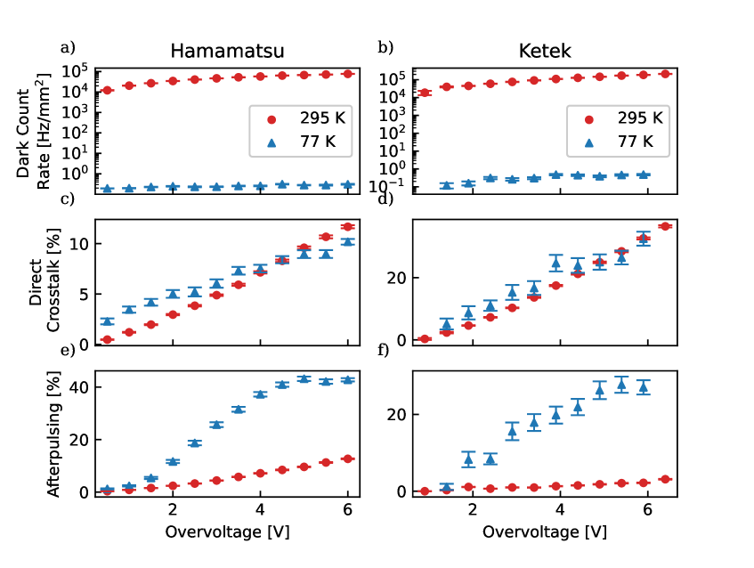
The direct cross-talk was also measured at a variety of overvoltages for both devices. The cross-talk probability is larger at cryogenic temperatures for both devices, but there is a cross-over point where it becomes equal to the room temperature cross-talk probability, as seen in Fig. 7(c) and Fig. 7(d). This is somewhat surprising as the cross-talk probability depends on the gain (via the number of secondary photons produced) and the avalanche triggering probability. The gain does not change significantly at cryogenic temperatures, but the avalanche triggering probability might, as was discussed in Section 4 [15]. The difference between room and liquid nitrogen temperature cross-talk probabilities is also not as substantial as it is for the afterpulsing.
The Hamamatsu and KETEK afterpulsing rates are significantly higher at liquid nitrogen temperatures, as shown in Fig. 7(e,f). A higher afterpulsing rate is potentially explained by the increased charge trapping lifetime at cryogenic temperatures: trapped carriers are more likely to be re-released while the cell is recovering and are thus more likely to trigger an afterpulse [19]. In addition to charge trapping re-releases, afterpulsing can also occur due to secondary carriers drifting from the substrate into the recharging SPAD [20]. This type of afterpulsing could also increase due to increased mobility of charge carriers at cryogenic temperatures and longer SPAD recovery times: carriers in the bulk silicon are more easily drifted into the active region and trigger an afterpulse [21]. Fig. 2d shows that the higher afterpulsing rate degrades of the Hamamatsu charge spectrum at liquid nitrogen temperatures. A similarly high cryogenic afterpulsing rate for a Hamamatsu device was recently reported in [22].