Interplay between domain walls and magnetization curling induced by chemical modulations in cylindrical nanowires
Abstract
Cylindrical magnetic nanowires have been proposed as a means of storing and processing information in a 3D medium, based on the motion of domain walls (DWs). Introducing short chemical modulations in such wires would allow for reliable digital control of DWs. Here, we outline the intricate physics of the interaction of domain walls with modulations to control their motion, combining micromagnetic simulations and experimental evidence. This interaction combines a long-range moderate magnetostatic repulsion with a local energy well. The latter depends on the respective circulation sense of magnetization in the domain wall and modulation. We also show that a modulation has the ability to switch the internal circulation of a DW upon its propagation, thereby acting as a polarizing component and opening the possibility to exploit not only the position of walls, but also their internal structure.
IMDEA Nanociencia, Campus de Cantoblanco, 28049 Madrid, Spain. \alsoaffiliationDpto. de Física de Materiales, Universidad Complutense de Madrid, 28040 Madrid, Spain. \alsoaffiliationDpto. de Física de Materiales, Universidad Complutense de Madrid, 28040 Madrid, Spain.
Cylindrical nanowires made of a soft-magnetic material are a textbook case for investigating magnetization dynamics in a three-dimensional geometry. Their magnetic textures are determined by the nanowire’s geometrical and compositional features, as well as by their magnetic history. While the uniaxial shape anisotropy favors an axial magnetization state, magnetic charges occurring at the wire terminations can induce end domains. Theory predicts that when the diameter is larger than circa seven times the dipolar exchange length, , the magnetization rotates around the wire axis in the end domains, which is commonly referred to as curling or vortex state1, 2, 3, 4. This configuration decreases magnetostatic energy at the expense of exchange energy, by converting part of the surface charges into volume charges. It is worth noting that extended curling domains may also arise in nanowires with magnetocrystalline anisotropy promoting azimuthal magnetization, as observed in CoNi alloys5, single-crystalline hcp Co6, 7, 8 or single-crystal CVD Ni wires9. However, we do not cover this specific case in the present manuscript.
There have been several experimental proofs of end curling: a decrease in remanence with increasing diameter10, more rounded hysteresis loops measured with the Kerr effect than with global magnetometry11, quantitative analysis using magnetic force microscopy12, or direct imaging with photo-emission electron microscopy13. Curling also occurs in other situations where axial magnetization gives rise to magnetic charges. One such scenario involves diameter modulation, as observed for nanowires made of FeCoCu14, single-crystal Ni15, NiFe alloys 16, 17, or Ni18, 19. Another case is the axial modulation of material, resulting in a mismatch of magnetization, such as in Fe20Ni80/Fe80Ni2020, 21, Ni/Co22, 23, 24, or Co/Cu25. The existence of curling textures is particularly relevant with the emergence of spintronic investigations of nanowires26, 27, 28, 29, 21, 30, 31, 32. Indeed, the axial charge current gives rise to an Œrsted field, which directly couples to curling textures and may assist nucleation33 or switch the sign of curling21.
Magnetic domain walls in cylindrical nanowires can manifest as one of two types: a Transverse-Vortex Wall (TVW) or a Bloch-Point Wall (BPW)4, 34. The characteristic feature of the TVW is a transversal magnetization component with respect to the wire axis, which implies the existence of two areas on the outer surface of the wire where , where is the unit vector normal to the surface. At these locations, the tangential magnetization takes the form of a vortex-antivortex pair35. The BPW is characterized by a curling magnetization around the wire axis and a magnetic singularity at its core, known as the Bloch point36, 37, 38. A feature that clearly distinguishes its topology from that of the TVW is the absence of any point on the wire surface with , although a radial magnetization component may arise to reduce magnetostatic effects related to the head-to-head or tail-to-tail domains.
The first experimental evidence of a BPW and a TVW in cylindrical nanowires was provided by shadow XMCD-PEEM microscopy in 201439. Subsequent studies include investigations of the possible transformation of the wall type under axial magnetic fields40 or under current pulses, where it was demonstrated BPW velocities in excess of and the switching of BPW curling with the Œrsted field27, 29.
Therefore, both chemical modulations and BPWs involve curling of magnetization around the wire axis, and in both cases the sign (circulation sense) can be switched with an anti-parallel Œrsted field 21, 27, 29. The similarity of their features naturally raises the question of how these two objects interact with each other. This question is particularly relevant since chemical modulations have been proposed as engineered sites to control domain walls in nanowires. In this manuscript, we examine this interaction, both experimentally and with micromagnetic simulations at rest and under the stimulus of an applied axial magnetic field. We shed light on the roles of exchange and dipolar energy, in order to understand the different mechanisms involved in domain wall pinning and propagation through a chemical modulation. A special focus is given to the significance of the respective circulations of the wall and modulation, which can either be parallel () or antiparallel ().
0.1 Energy landscape of a DW at a modulation
0.1.1 Micromagnetic simulations
In the following, we describe the energetics of a domain wall in a nanowire. Due to the mostly one-dimensional nature of nanowires, their energy landscape may be reduced to one dimension as in the Becker-Kondorski description41. For nanowires with homogeneous composition, ideally, the domain wall energy does not depend on its position, as long as it is far enough from the wire ends. However, in practice, domain walls may be pinned at specific locations, such as material defects or grain boundaries42, 43, 44. The introduction of chemical modulations aims to modify the domain wall energy landscape, allowing controlled pinning sites to be established if the artificial pinning strength exceeds that related to material defects. In micromagnetic simulations, one method to extract the energy landscape is to monitor the domain wall energy during its slow drift free of external forces under large damping so that it remains under quasistatic conditions at all times. This approach was successfully used for a diameter-modulated nanowire 45. However, in the present case, such a method cannot be easily applied, as the profile of the energy landscape may be non-monotonous so that the drift does not cover all positions. Instead, we applied an axial external magnetic field to move the domain wall towards the chemical modulation. The damping coefficient was set to to be as close to equilibrium as possible and in a quasi-static situation. Both methods are expected to coincide as long as the applied field does not significantly affect the internal structure of the domain wall, such as its width.
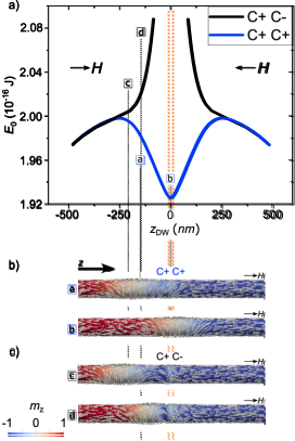
We consider a diameter Permalloy (Fe20Ni80) nanowire with a -long Fe80Ni20 chemical modulation at , in two situations: parallel and anti-parallel curling circulations of BPW and modulation, and respectively. The domain wall is pushed towards the modulation under the application of an external magnetic field oriented along or for z or z, respectively, with magnitude increasing in small steps. The initial circulation of the BPW is chosen with the same sign as the direction of motion, so that it is the stable one during dynamics and thus does not switch spontaneously during motion46. The internal energy, i.e., the sum of the dipolar and exchange energy: , is displayed versus BPW position (zDW) on Figure 1a. is computed as the intercept of the three iso-surfaces of the magnetization field: , and 47. Figure 1b and Figure 1c show outer views of the micromagnetic simulation at selected time steps. At a long distance from the modulation, typically or more, both curves overlap and reveal a repulsive interaction. To the contrary, at shorter distances, the respective circulations matter: the repulsion keeps increasing for opposite circulations, giving rise to an energy barrier, while the modulation acts as a local potential well for identical circulations. This can be understood as follows. (i) At long distances between the BPW and the modulation the interaction is independent of their relative circulations. This is consistent with the known fact that circulations of curling structures do not interact with one another via dipolar interactions48, as the magnetic potential does not depend on the sign of circulation. The repulsion results from the interaction of the positively-charged head-to-head BPW with the dipolar field of the modulation, whose positively-charged interface is the one closest to the wall21. The same repulsion would apply for a negatively charged tail-to-tail BPW, giving rise to a neighboring negatively-charged modulation interface. (ii) At short distances, the magnetization textures of the BPW and the modulation overlap and interact directly via exchange: magnetization gradients decrease for parallel circulation, while they increase for antiparallel circulations (see Figure 1b), which translates into a decrease (resp. increase) of exchange energy. This, again, is consistent with previous reports on the interaction of curling end structures in short nanotubes48.
0.1.2 Experimental evidence of DW pinning and repulsion
We have experimentally probed the effectiveness of chemical modulations as pinning sites for domain walls, previously nucleated by applying a magnetic field of around perpendicular to the wire axis or by injecting a -long pulse of current with amplitude . We image the magnetization states in the wires with either full field or scanning Transmission X-ray microscopy, as well as with X-ray ptychography, all combined with XMCD. The combination of high spatial resolution and direct probing of magnetization enables the extraction of unambiguous information about the DW type and inner structure.
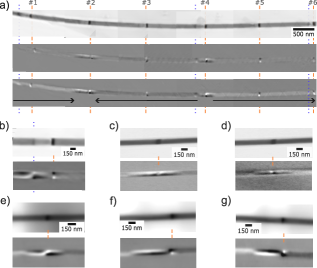
Figure 2a shows composite transmission amplitude ptychographic reconstruction and XMCD images at the Fe L3 edge of a -diameter Permalloy nanowire with periodic -long Fe80Ni20 chemical modulations. The darker regions in the transmission image marked with orange dashed lines are the Fe-rich chemical modulations (higher absorption). A closer look reveals a depletion in the Fe content at the left of some of the chemical modulations, extending over a few hundreds of nanometers and ending with a short Fe-rich minor modulation (see blue dotted line, e.g., modulation ). This material inhomogeneity arises from an instability occurring during the electroplating process. Based on this finding, the synthesis was revisited to avoid this defect. Corresponding images will be shown later on, but magnetic images of this first generation of wires are informative on their own.
The XMCD images in Figure 2a correspond to the wire axis perpendicular to the X-ray beam (middle), and with a offset (bottom). The former is insensitive to the axial magnetization component. Therefore, the neutral gray level in the Permalloy segments reveals that they are uniformly magnetized along the axis. In contrast, a strong dark/bright contrast arises on either side of the wire at every modulation, indicative of magnetization curling around the axis21. Note that for a given magnetization component, we expect XMCD to be stronger for Fe-rich areas due to the stronger absorption13, so that the displayed contrast does not reflect quantitatively the magnetization state. The image with the tilted sample offers a light dark and bright contrast reflecting axial magnetization in the segments, revealing the occurrence of three domains (black arrows). The stronger magnetic contrast at modulations and can now be understood as the signature of BPWs, while the lighter contrast at the other modulations simply reflects spontaneous curling of magnetization due to the mismatch of magnetization magnitude. The two DWs pinned at modulations and confirm the potential of modulations to pin DWs. A close look shows that the DW is centered exactly on the main modulation, while the secondary chemical modulation also induces a slight curling, which may be either parallel (modulation ) or antiparallel (modulation ) to that of the BPW. This complex modulations can give rise to other pinning situations, such as illustrated in Figure 2b. Here, the DW is of TVW type and is pinned at the secondary chemical modulation. This highlights the generality of the pinning potential of modulations, regardless of their strength and the type of DW. One may wonder whether this configuration results from the exchange-driven repulsion between the modulation and the opposite circulation on the right side of the TVW, outlined previously, however, the existence of the secondary modulation biases the discussion.
To get a conclusive view, we now examine the situation of symmetric chemical modulations, i.e., after refining the synthesis process, and with a variety of wire diameters and lengths of chemical modulation (Figure 2c-g). Domain walls of either BPW (Figure 2c-d) or TVW type (Figure 2e) can be pinned exactly at the modulation. Note that Figure 2c and Figure 2d are of the same modulation imaged at the Fe L3 and Fe L2, respectively, in a case where a too high absorption at the L3 edge resulted in saturation and thus absence of magnetic contrast13. BPWs can also be found very close to a modulation, in situations where the sign of circulation of the DW and modulation are opposite (Figure 2f-g). This is consistent with the micromagnetic simulations which showed that modulations can give rise to a potential well to pin DWs, but in case of opposite circulation situation there exists a strong repulsive potential, so that the DW stops just before the modulation.
0.2 Propagation of DWs through modulations
We now consider the magnetization process of domain-wall motion across a modulation under the stimulus of an external axial magnetic field, for both parallel and antiparallel magnetization circulation between BPW and modulation.
0.2.1 The case of identical circulations – Smooth propagation
In this section, we consider the situation where the BPW and the chemical modulation exhibit the same sign of circulation. We start with micromagnetic simulations of a diameter Permalloy nanowire, with either a or a -long chemical modulation. The initial state is a head-to-head BPW located at , which we push towards the modulation by applying a positive magnetic field. The strength of the magnetic field is increased in the form of plateaus of length and rising magnitude. The damping coefficient is , to mimic a quasistatic situation. We chose a positive circulation in both modulation and BPW, which is the stable one during motion along in a homogeneous wire 46.
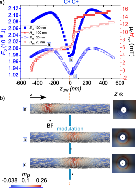
Figure 3a shows the internal energy of the system as a function of . The open blue symbols depict the scenario of a chemical modulation with a length of , while the filled blue symbols depict the scenario with a chemical modulation with a length of . The red symbols indicate the linearly-increasing strength of the magnetic field, with plateaus of duration . The two energy profiles are qualitatively similar, with a well at the modulation and long-distance repulsion, consistent with Figure 1a. Initially, the DW is located on the left-hand side of the modulation in the repulsive area, and the field needs to be increased to about to overcome the axial gradient of internal energy (Note that the DW is already continuously drifting during each of the -long plateaus at the top of the energy barrier, around , so that the value of the magnetic field when at this position is an upper value of the propagation field). Then, the DW remains pinned close to the bottom of the energy well over a wide range of values of applied field, which is illustrated by the sharp slope of the red curves. Finally, the DW depins from the modulation and starts drifting again to the right. The depinning field is and for the short and long modulations, respectively. The propagation and depinning fields more or less reflect the value of steepest slope of internal energy, consistent with the Becker-Kondorsky model. In the case of the longer modulation the internal energy is shifted upwards even when the DW is away from the modulation, reflecting the higher cost associated with curling in the longer segment21. The upward shift is reduced at rest likely because most of the curling of the BPW fits within the modulation, so that the cost of exchange required anyway by the modulation, benefits the BPW. This results in a deeper energy well for the longer modulation, and thus a larger depinning field. Finally, note that the energy peak for is higher than for , contrary to the energy landscape computed in Figure 1a. This is probably related to the slight change of the inner structure of the BPW due to the applied field, which is different when entering versus leaving the modulation.
As the peripheral curling and the Bloch point may follow different dynamics during the motion of a BPW49, it is interesting to track the Bloch point during the propagation/pinning/depinning process, which is illustrated in Figure 3b. On the left, an external view of the magnetization field at the wire surface is shown with gray arrows. The background color codes the radial component of magnetization , and thus the location of the wall, as it results from the associated head-to-head charges46. Below each view, the black square indicates the axial position of the Bloch point. On the right side, an internal surface view through the nanowire illustrates the radial position of the Bloch point. The Bloch point deviates only slightly in a minor fashion from the center of mass of the wall. It is ahead of the wall in the repulsive region, and tends to be pinned at interfaces of the modulation. Hence, we conclude that a BPW propagates smoothly through a chemical modulation, when their circulation senses are parallel.
0.2.2 Experimental evidence of BPW depinning, motion and repinning
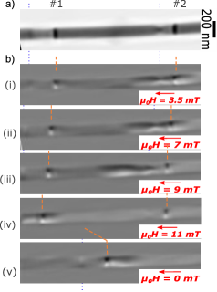
In the following, we provide experiments supporting the micromagnetic predictions. We consider a -diameter Permalloy nanowire with two -long chemical modulations separated by a distance of , shown in Figure 4. Note that this is a situation of asymmetric modulations, with a Fe-depleted segment on the left-hand side of the modulation, ending with a narrow Fe-rich secondary modulation. The initial state is a head-to-head DW located at the right modulation, labeled . There is no DW at the left modulation, labeled , but its circulation is of the same sign. We apply a dc axial magnetic field, that tends to move the DW to that second modulation. Initially, the domain wall center seems to lie between the main and the secondary modulations of . At a critical field of , the BPW is depinned and moves left, still being connected to the secondary modulation. At , the BPW propagates along the entire Permalloy segment until modulation . Upon removal of the magnetic field, the BPW relaxes, shifting slightly to the right side. This slight shift may be attributed to the opposing curling circulation in the secondary modulation of , inducing a repulsion of the BPW towards the opposite direction. Therefore, we have confirmed experimentally the order of magnitude of the pinning and depinning strength at the modulations for parallel circulations. The data also illustrates controlled pinning, stronger than the intrinsic pinning on material defects along the Permalloy segments.
0.2.3 The case of opposite circulations – Modulations as a polarizing component
In addition to the above, we now consider the propagation of a BPW through a chemical modulation, with initially anti-parallel circulation. We expect a behavior different from the case of identical circulation, as the modulation should act as an energy barrier to the domain wall (Figure 1). The initial configuration is a head-to-head BPW at and a chemical modulation at z. The magnetic field strength is increased linearly, and a damping coefficient is used, in order to mimic a quasistatic situation. The circulation is initially positive in the BPW, which is the stable one during motion along in a homogeneous wire.
Figure 5a shows the DW internal energy during its propagation through the modulation, along with selected micromagnetic views and tracking of the Bloch point. The left and right panels correspond to a chemical modulation length of and , respectively. The energy profiles are similar to those in Figure 1 for , i.e., an energy barrier due to the magnetostatic-driven repulsion. However, the situation changes drastically at later stages, although reminiscent of a potential well for . First, the profiles are largely asymmetric when comparing the left and right sides of the modulation. Second, discontinuities of the internal energy are observed. Third, the propagation field is considerably larger than for identical circulations , e.g., for a -long modulation. For the case of a -long modulation, the depinning field reaches . All this hints at a drastically-different propagation mechanism than in the case of , which we examine now in more detail.
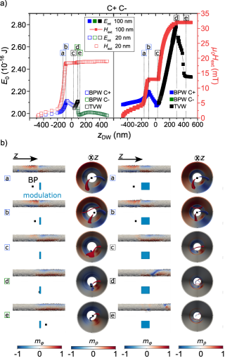
Figure 5b displays the micromagnetic simulations outer views and surface inner views. The color code denotes the azimuthal and radial magnetization , respectively. The black square indicates the Bloch point position, while the elongated blue rectangle denotes the chemical modulation. Labels on the left correspond to configurations at various zDW values indicated by the black dashed lines in Figure 5a. Upon analyzing the temporal evolution of these configurations, several key observations emerge: initially, the BPW and modulation display opposite contrast due to their antiparallel circulations (labeled as ). At this point the inner view presents isolines in the bulk connecting the surface to the Bloch point. As the BPW approaches the modulation it shrinks while increasing in energy (blue symbols in Figure 5a). At the point labeled as , a new isoline crosses the bulk, ending by the disappearance of the blue isoline with the Bloch point, resulting in a TVW-type DW (labeled as ). Note that between and the topology of the wall remains that of a BPW 29, 50. The TVW-type configuration is represented by the black symbols in Figure 5a. Following this, the evolution diverges for short and large modulation lengths. For short modulations of length (left panel), the energy increases reaching a maximum of , at which point the Bloch point reappears in the volume and pins onto the chemical modulation (labeled as ). At this stage, the Bloch point lags behind the BPW (see state in the outer-micromagnetic view), indicating a state far from equilibrium. The equal contrast in wall and modulation illustrates a reversal of BPW circulation. The BPW configuration with negative circulation is represented by the green symbols in Figure 5a, which indicate the subsequent decrease in energy associated with depinning (labeled as ), followed by a potential well for parallel circulations, as illustrated in Figure 1. In contrast, for a modulation, the energy increases further, up to , until the TVW-type configuration propagates through the modulation (labeled as ). This is followed by a decrease in energy until the TVW depins from the modulation and propagates freely along (labeled as ). Subsequently, the Bloch point re-enters the volume, and a BPW of reversed circulation keeps propagating (not shown). The larger deppining field induces a high excitation to the system causing the re-injection of the Bloch point in the volume (or transformation to BPW ) at .
To better understand the microscopic mechanism of the domain wall transformation, and link it to the non-trivial energy evolution in Figure 5, it is helpful to perform a topological analysis50. To mimic a more realistic situation, the simulations were conducted with an and an axial magnetic field of . The tracking of the volume and surface singularities was performed by using a post-processing tool. Figure 6a displays the outer micromagnetic view of the initial state. The color code corresponds to the azimuthal magnetization, being red for the BPW curling along and blue for the chemical modulation magnetized along . The three-dimensional view in Figure 6b displays the trace of the Bloch point (in black) and surface vortex-antivortex pairs (in colors). The chemical modulation is represented by the grey disk. The displacement of the Bloch point occurs along the wire axis as is well known for domain wall motion in an homogeneous nanowire51. Upon approaching the chemical modulation, the Bloch point travels towards the surface until it annihilates with a surface vortex or antivortex (labeled ). Subsequently, an azimuthal displacement of the latter occurs until a Bloch point is injected into the volume (labeled ) and propagates trough the chemical modulation.
The evolution of the two vortex-antivortex pairs is displayed in Figure 6d along the axial and azimuthal directions. It is important to note that here we depict a zoom of the critical events, while the Bloch point (represented by the black symbols) has existed in the system since . The first pair nucleated V - AV shows positive polarity (red and orange lines), whereas the second pair V - AV shows negative polarity (blue and green lines). Within each V-AV pair, the vortex and antivortex move away from each other along the azimuthal direction. We believe that the polarity of the first pair appearing can be understood as it matches the polarity of the head-to-head BPW, and also the one favored by the chirality of the Landau–Lifshitz–Gilbert (LLG) equation via . The reason for the opposite polarity of the second pair is probably to reduce the global magnetostatic energy. Overall, the detailed process involves the Bloch point reaching the surface at the moment when the vortex with negative polarity V (blue) and the antivortex with positive polarity AV (orange) merge. At this precise moment, only V and AV remain in the system far from each other. Later, a Bloch Point with negative polarity re-enters in the volume as V and AV annihilate.
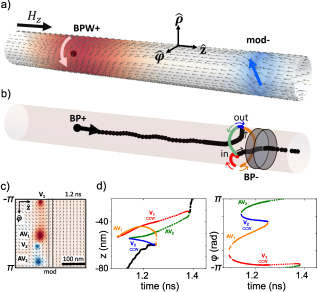
The phenomenon of BPW circulation switching upon crossing a chemical modulation under a magnetic field represents a novel discovery. Nevertheless, the underlying mechanism mirrors the one reported in ref Riz et al. 29 for BPW switching in an homogeneous nanowire driven by an anti-parallel Oersted field, sharing the same topological features. We can draw an analogy between this phenomenon and the mechanisms of coherent reversal versus nucleation-propagation for the magnetization reversal of magnetic systems: the switching of BPW circulation via the homogeneous rise of to on the wire periphery would imply a substantial dipolar energy cost. Instead, here we observe the local nucleation of an area with , which then propagates around the perimeter through the motion of surface vortex-antivortex pairs along opposite azimuthal directions.
Regarding the switching of BPW in a homogeneous or in chemically-modulated system, it is important to note the distinctions between the two scenarios. The unrolled map of Figure 6c illustrates that the vortex-antivortex pairs nucleate always on the same side of the BPW, between the BPW interface and the chemical modulation. This contrasts with the scenario of the Œrsted field induced BPW switching on a homogeneous nanowire (without chemical modulation), where one vortex or antivortex of same polarity appears at each side of the wall29. Here, the strong exchange interaction with the opposite circulation of the modulation acts in a very similar fashion to an Œrsted field, but on one side only of the DW.
0.3 Conclusion
In summary, we have experimentally outlined and analyzed, through micromagnetic simulations, the interaction between higher-magnetization chemical modulations and Bloch Point walls (BPWs) in cylindrical nanowires. These modulations act as local potential wells, that effectively pin domain walls due to their shared azimuthal curling, thereby lowering the total energy of the system. However, the mechanism of propagation through a modulation is complex. At distances larger than the BPW width, the interaction is primarily repulsive, driven by magnetostatics. As the distance decreases, exchange interactions become significant, breaking the degeneracy between cases of identical or opposite circulation senses in the wall and the modulation. In the former case, the BPW can propagate through the modulation relatively unchanged, although the depinning field is higher than the field required to push the wall into the energy well of the modulation. For opposite circulations, the modulation forces the BPW to change its circulation before propagation can occur, effectively acting as a polarizing device. This process involves the annihilation/re-nucleation of a Bloch point and a transient topology state of a transverse-vortex wall, a phenomenon reported here for the first time. This process is similar, and thus consistent, with the change of domain wall type in homogeneous nanowires driven by field or Œrsted-field, shedding light on the generality of the phenomenon. These findings open the possibility of utilizing chemical modulations as a polarizing component, thereby allowing the control of the internal structure of domain walls.
0.4 Methods
Permalloy (Fe20Ni80) cylindrical nanowires with Fe-rich chemical modulations were synthesized by single-bath template-assisted electrochemical deposition. Nanoporous anodic aluminum oxide (AAO) templates were prepared by hard anodization of Al disks (Goodfellow, in purity) in a water-based solution of oxalic acid () and ethanol (), applying of anodization voltage at for . The remaining Al was etched with an aqueous solution of CuCl2 () and HCl (), the oxide barrier was removed and the pores opened to a final diameter of with H3PO4 (5 % vol.).
The growth conditions were similar to those described in ref Ruiz-Gómez et al. 52. For chemical modulations with a length below , the composition was Fe65Ni35, while for lengths above , the composition was Fe80Ni20. After the electrochemical growth, the AAO templates were dissolved in H3PO4() and H2CrO4(). Then, the nanowires were dispersed on thick Si3N4 windows to allow for transmission microscopy. To nucleate domain walls, nanowires were contacted electrically using laser lithography in order to allow the injection of bandwidth electric pulses. Resistivity values obtained are around . To prevent sample oxidation and to increase thermal transfer to the Si3N4, a -thick layer of Al2O3 was deposited on the device by Atomic Layer Deposition (ALD). Additionally, of Al was deposited on the backside of the substrate.
The wires were imaged with X-ray Magnetic Circular Dichroism (XMCD) coupled to Transmission X-ray Microscopy (TXM) 53 at the MISTRAL beamline of ALBA Synchrotron and by X-ray ptychography54, 55, 56 at HERMES STXM beamline of SOLEIL synchrotron. The photon energy was set to the Fe L3 absorption edge, and the sample holder could be rotated from the plane normal to the X-ray incidence in order to be sensitive to both axial and azimuthal magnetization components. During TXM imaging, series of about 64 images per polarity were were acquired, registered and averaged in order to increase the signal-to-noise ratio, while keeping under control the loss of spatial resolution due to time drift. Ptychographic reconstruction was carried out using the open-source PyNX software developed at the European Synchrotron Radiation Facility 57. If not initially present, DWs were nucleated in situ by applying a -long pulse of current with amplitude . We performed micromagnetic simulations with the mumax3 code58. The system considered is a cylindrical Permalloy nanowire of diameter and length, with a -long or -long Fe80Ni20 chemical modulation at its center. In order to mimic an infinite wire, the magnetic charges at the wire ends were removed numerically. The mesh size used was . The following material parameters were used59: spontaneous magnetization for the Permalloy segments, for the chemical modulation, single exchange stiffness for all materials and zero magnetocrystalline anisotropy. The choice of an identical value for exchange stiffness stems from the similarity of ordering temperature for the two compositions. The resulting dipolar exchange lengths are and , respectively. To study static or quasi-static dynamics a damping term of was used. The initial state considered was a BPW at z and a chemical modulation centered at z . Circulations of both the BPW and the modulation are defined arbitrarily with respect to , and labeled for positive and for negative.
When the tracking of topological elements characterizing the type of wall is required (Bloch point for BPW, surface vortex/antivortex for the TVW), we use an in-house post-processing tool, developed specifically for tetrahedron-based finite-elements 50. Therefore, in this case the micromagnetic simulations were conducted with feeLLGood code 60, 61, 62, 63, a home-made micromagnetic code based on finite-element methods.
This work received financial support from the French RENATECH network, implemented at the Upstream Technological Platform in Grenoble PTA (ANR-22-PEEL-0015), and from the French National Research Agency (Grant No. ANR-17-CE24-0017 MATEMAC-3D; Grant ANR-22-CE24-0023 DIWINA), from the Spanish (MCIN/AEI/10.13039/501100011033 through Projects PID2020-117024GB-C43, TED2021-130957B-C52 and CEX2020- 001039-S). S. R-G acknowledges support from the Humboldt foundation grant 1223621 and Marie Curie fellowship grant GAP-101061612. M. F. acknowledges the funding from MICIN through grant number PID2021-122980OB-C54. We acknowledge support from the team of the Nanofab platform (CNRS Néel institut), from the ALBA in-house research program and MISTRAL and CIRCE beamlines and from the SOLEIL HERMES beamline.
References
- Arrott et al. 1979 Arrott, A. S.; Heinrich, B.; Aharoni, A. Point singularities and magnetization reversal in ideally soft ferromagnetic cylinders. IEEE Trans. Magn. 1979, 15, 1228
- Hinzke and Nowak 2000 Hinzke, D.; Nowak, U. Magnetization switching in nanowires: Monte Carlo study with fast Fourier transformation for dipolar fi. J. Magn. Magn. Mater. 2000, 221, 365
- Zeng et al. 2002 Zeng, H.; Skomski, R.; Menon, L.; Liu, Y.; Bandyopadhyay, S.; Sellmyer, D. J. Structure and magnetic properties of ferromagnetic nanowires in self-assembled arrays. Phys. Rev. B 2002, 65, 134426
- Hertel 2002 Hertel, R. Computational micromagnetism of magnetization processes in nickel nanowires. J. Magn. Magn. Mater. 2002, 249, 251
- Bran et al. 2017 Bran, C.; Fernandez-Roldan, J. A.; Palmero, E. M.; Berganza, E.; Guzman, J.; del Real, R. P.; Asenjo, A.; Rodriguez, A. F.; Foerster, M.; Aballe, L.; Chubykalo-Fesenko, O.; Vazquez, M. Direct Observation of Transverse and Vortex Metastable Magnetic Domains observed in Cylindrical Nanowires. Phys. Rev. B 2017, 96, 125415
- Vila et al. 2009 Vila, L.; Darques, M.; Encinas, A.; Ebels, U.; George, J.-M.; Faini, G.; Thiaville, A.; Piraux, L. Magnetic vortices in nanowires with transverse easy axis. Phys. Rev. B 2009, 79, 172410
- Ivanov et al. 2013 Ivanov, Y. P.; Vivas, L. G.; Asenjo, A.; Chuvilin, A.; Chubykalo-fesenko, O.; Vazquez, M. Magnetic structure of a single-crystal hcp electrodeposited cobalt nanowire. Europhys. Lett. 2013, 102, 17009
- Chen et al. 2016 Chen, F.; Wang, F.; Jia, F.; Li, J.; Liu, K.; Huang, S.; Luan, Z.; Wu, D.; Chen, Y.; Zhu, J.; Peng, R.-W.; Wang, M. Periodic magnetic domains in single-crystalline cobalt filament arrays. Phys. Rev. B 2016, 93, 054405
- Kan et al. 2018 Kan, J. J.; Lubarda, M. V.; Chan, K. T.; Uhlíř, V.; Scholl, A.; Lomakin, V.; Fullerton, E. E. Periodic chiral magnetic domains in single-crystal nickel nanowires. Phys. Rev. Mater. 2018, 2
- Chien et al. 2002 Chien, C. L.; Sun, L.; Tanase, M.; Bauer, L. A.; Hultgren, A.; Silevitch, D. M.; Meyer, G.; Searson, P.; Reich, D. H. Electrodeposited magnetic nanowires: arrays, field-induced assembly, and surface functionalization. J. Magn. Magn. Mater. 2002, 249, 146
- Wang et al. 2008 Wang, T.; Wang, Y.; Fu, Y.; Hasegawa, T.; Oshima, H.; Itoh, K.; Nishio, K.; Masuda, H.; Li, F. S.; Saito, H.; Ishio, S. Magnetic behavior in an ordered Co nanorod array. Nanotechnology 2008, 19, 455703
- Vock et al. 2014 Vock, S.; Hengst, C.; Wolf, M.; Tschulik, K.; Uhlemann, M.; Sasvari, Z.; Makarov, D.; Schmidt, O. G.; Schultz, L.; Neu, V. Magnetic vortex observation in FeCo nanowires by quantitative magnetic force microscopy. Appl. Phys. Lett. 2014, 105, 172409
- Jamet et al. 2015 Jamet, S.; Col, S. D.; Rougemaille, N.; Wartelle, A.; Locatelli, A.; Menteş, T. O.; Burgos, B. S.; R.Afid; Cagnon, L.; Bachmann, J.; Bochmann, S.; Fruchart, O.; ; Toussaint, J. C. Quantitative analysis of shadow X-ray Magnetic Circular Dichroism Photo-Emission Electron Microscopy. Phys. Rev. B 2015, 92, 144428
- Iglesias-Freire et al. 2015 Iglesias-Freire, O.; Bran, C.; Berganza, E.; Mínguez-Bacho, I.; Magén, C.; Vázquez, M.; Asenjo, A. Spin configuration in isolated FeCoCu nanowires modulated in diameter. Nanotechnology 2015, 26, 395702
- Bran et al. 2016 Bran, C.; Berganza, E.; Palmero, E. M.; Fernandez-Roldan, J. A.; Del Real, R. P.; Aballe, L.; Foerster, M.; Asenjo, A.; Rodríguez, A. F.; Vazquez, M. Spin configuration of cylindrical bamboo-like magnetic nanowires. J. Mater. Chem. C 2016, 4, 978–984
- Chandra Sekhar et al. 2012 Chandra Sekhar, M.; Liew, H. F.; Purnama, I.; Lew, W. S.; Tran, M.; Han, G. C. Helical domain walls in constricted cylindrical NiFe nanowires. Appl. Phys. Lett. 2012, 101, 152406
- Salem et al. 2013 Salem, M. S.; Sergelius, P.; Corona, R. M.; Escrig, J.; Görlitz, D.; Nielsch, K. Magnetic properties of cylindrical diameter modulated Ni80Fe20 nanowires: interaction and coercive fields. Nanoscale 2013,
- Nasirpouri et al. 2019 Nasirpouri, F.; Peighambari-Sattari, S.-M.; Palmero, C. B. E. M.; Eguiarte, E. B.; Vazquez, M.; Patsopoulos, A.; Kechrakos, D. Geometrically designed domain wall trap in tri-segmented nickel magnetic nanowires for spintronics devices. Sci. Rep. 2019, 9, 1–11
- Allende et al. 2009 Allende, S.; Altbir, D.; Nielsch, K. Magnetic cylindrical nanowires with single modulated diameter. Phys. Rev. B 2009, 80, 174402
- Ruiz-Gómez et al. 2020 Ruiz-Gómez, S.; Fernández-González, C.; Martínez, E.; Raposo, V.; Sorrentino, A.; Foerster, M.; Aballe, L.; Mascaraque, A.; Ferrer, S.; Pérez, L. Helical surface magnetization in nanowires: the role of chirality. Nanoscale 2020, 12, 17880–17885
- Álvaro-Gómez et al. 2022 Álvaro-Gómez, L. et al. Micromagnetics of magnetic chemical modulations in soft-magnetic cylindrical nanowires. Phys. Rev. B 2022, 106, 054433
- Ivanov et al. 2016 Ivanov, Y. P.; Chuvilin, A.; Lopatin, S.; Kosel, J. Modulated Magnetic Nanowires for Controlling Domain Wall Motion: Toward 3D Magnetic Memories. Am. Chem. Soc. Nano 2016, 10, 5326
- Berganza et al. 2017 Berganza, E.; Jaafar, M.; Bran, C.; Fernández-Roldán, J. A.; Chubykalo-Fesenko, O.; Vázquez, M.; Asenjo, A. Multisegmented Nanowires: a Step towards the Control of the Domain Wall Configuration. Sci. Rep. 2017, 7, 11576
- Andersen et al. 2021 Andersen, I. M.; Wolf, D.; Rodriguez, L. A.; Lubk, A.; Oliveros, D.; Bran, C.; Niermann, T.; Rößler, U. K.; Vazquez, M.; Gatel, C.; Snoeck, E. Field tunable three-dimensional magnetic nanotextures in cobalt-nickel nanowires. Phys. Rev. Research 2021, 3, 033085
- Reyes et al. 2016 Reyes, D.; Biziere, N.; Warot-Fonrose, B.; Wade, T.; Gatel, C. Magnetic Configurations in Co/Cu Multilayered Nanowires: Evidence of Structural and Magnetic Interplay. Nano Lett. 2016, 16, 1230–1236
- Franchin et al. 2011 Franchin, M.; Knittel, A.; Albert, M.; Chernyshenko, D. S.; Fischbacher, T.; Prabhakar, A.; Fangohr, H. Enhanced spin transfer torque effect for transverse domain walls in cylindrical nanowires. Phys. Rev. B 2011, 84, 094409
- Schöbitz et al. 2019 Schöbitz, M. et al. Fast domain walls governed by topology and Œsted fields in cylindrical magnetic nanowires. Phys. Rev. Lett. 2019, 123, 217201
- Fernandez-Roldan et al. 2020 Fernandez-Roldan, J. A.; del Real, R. P.; Bran, C.; Vazquez, M.; Chubykalo-Fesenko, O. Electric current and field control of vortex structures in cylindrical magnetic nanowires. Phys. Rev. B 2020, 102, 024421
- Riz et al. 2021 Riz, A. D.; Hurst, J.; Schöbitz, M.; Thirion, C.; Bachmann, J.; Toussaint, J. C.; Fruchart, O.; Gusakova, D. Mechanism of fast domain wall motion via current-assisted Bloch-point domain wall stabilization. Phys. Rev. B 2021, 103, 054430
- Fernandez-Roldan and Chubykalo-Fesenko 2022 Fernandez-Roldan, J. A.; Chubykalo-Fesenko, O. Dynamics of chiral domain walls under applied current in cylindrical magnetic nanowires. APL Materials 2022, 10, 111101
- Moreno and Kosel 2022 Moreno, J. A.; Kosel, J. Current-induced zero-field domain wall depinning in cylindrical nanowires. Sci. Rep. 2022, 12
- Bran et al. 2023 Bran, C.; Fernandez-Roldan, J. A.; Moreno, J. A.; Fraile Rodríguez, A.; del Real, R. P.; Asenjo, A.; Saugar, E.; Marqués-Marchán, J.; Mohammed, H.; Foerster, M.; Aballe, L.; Kosel, J.; Vazquez, M.; Chubykalo-Fesenko, O. Domain wall propagation and pinning induced by current pulses in cylindrical modulated nanowires. Nanoscale 2023, 15, 8387–8394
- Otalora et al. 2015 Otalora, J. A.; Cortés-Ortuno, D.; Görlitz, D.; Nielsch, K.; Landeros, P. Oersted field assisted magnetization reversal in cylindrical core-shell nanostructures. J. Appl. Phys. 2015, 117, 173914
- Forster et al. 2002 Forster, H.; Schrefl, T.; Scholz, W.; Suess, D.; Tsiantos, V.; Fidler, J. Micromagnetic simulation of domain wall motion in magnetic nano-wires. J. Magn. Magn. Mater. 2002, 249, 181
- Jamet et al. 2015 Jamet, S.; Rougemaille, N.; Toussaint, J. C.; Fruchart, O. In Magnetic Nano- and Microwires: Design, synthesis, properties and applications; Vazquez, M., Ed.; Woodhead, 2015; Chapter Head-to-head domain walls in one-dimensional nanostructures: an extended phase diagram ranging from strips to cylindrical wires, pp 783–811
- Döring 1968 Döring, W. Point singularities in micromagnetism. J. Appl. Phys. 1968, 39, 1006
- Feldtkeller 1965 Feldtkeller, R. Mikromagnetisch stetige und unstetige Magnetisirungsverteilungen. Z. Angew. Physik 1965, 19, 530
- Malozemoff and Slonczewski 1979 Malozemoff, A. P.; Slonczewski, J. C. Magnetic domain walls in bubble materials; Academic press, 1979
- Da Col et al. 2014 Da Col, S.; Jamet, S.; Rougemaille, N.; Locatelli, A.; Menteş, T. O.; Burgos, B. S.; Afid, R.; Darques, M.; Cagnon, L.; Toussaint, J. C.; Fruchart, O. Observation of Bloch-point domain walls in cylindrical magnetic nanowires. Phys. Rev. B 2014, 89, 180405
- Wartelle et al. 2019 Wartelle, A.; Trapp, B.; Staňo, M.; Thirion, C.; Bochmann, S.; Bachmann, J.; Foerster, M.; Aballe, L.; Menteş, T. O.; Locatelli, A.; Sala, A.; Cagnon, L.; Toussaint, J.; Fruchart, O. Bloch-point-mediated topological transformations of magnetic domain walls in cylindrical nanowires. Phys. Rev. B 2019, 99, 024433, arXiv:1806.10918
- Kondorski 1937 Kondorski, E. On the nature of coercive force and irreversible changes in magnetisation. Phys. Z. Sowjetunion 1937, 11, 597
- Henry et al. 2001 Henry, Y.; Ounadjela, K.; Piraux, L.; Dubois, S.; George, J.-M.; Duvail, J.-L. Magnetic anisotropy and domain patterns in electrodeposited cobalt nanowires. Eur. Phys. J. B 2001, 20, 35
- Da Col et al. 2016 Da Col, S.; Jamet, S.; Staňo, M.; Trapp, B.; Denmat, S. L.; Cagnon, L.; Toussaint, J. C.; Fruchart, O. Nucleation, imaging, and motion of magnetic domain walls in cylindrical nanowires. Appl. Phys. Lett. 2016, 109, 062406
- Schöbitz et al. 2023 Schöbitz, M.; Novotný, O.; Trapp, B.; Bochmann, S.; Cagnon, L.; Thirion, C.; Massebœuf, A.; Mossang, E.; Fruchart, O.; Bachmann, J. A Material View on Extrinsic Magnetic Domain Wall Pinning in Cylindrical CoNi Nanowires. J. Phys. Chem. C 2023, 127, 2387–2397
- Riz et al. 2020 Riz, A. D.; Trapp, B.; Fernandez-Roldan, J.; Thirion, C.; Toussaint, J.-C.; Fruchart, O.; Gusakova, D. Magnetic Nano- and Microwires; Elsevier, 2020; pp 427–453
- Thiaville and Nakatani 2006 Thiaville, A.; Nakatani, Y. In Spin dynamics in confined magnetic structures III; Hillebrands, B., Thiaville, A., Eds.; Topics Appl. Physics; Springer: Berlin, 2006; Vol. 101; Chapter Domain-wall dynamics in nanowires and nanostrips, pp 161–205
- Andreas et al. 2014 Andreas, C.; Kákay, A.; Hertel, R. Multiscale and multimodel simulation of Bloch-point dynamics. Phys. Rev. B 2014, 89, 134403
- Wyss et al. 2017 Wyss, M.; Mehlin, A.; Gross, B.; Buchter, A.; Farhan, A.; Buzzi, M.; Kleibert, A.; Tütüncüoglu, G.; Heimbach, F.; Fontcuberta i Morral, A.; Grundler, D.; Poggio, M. Imaging magnetic vortex configurations in ferromagnetic nanotubes. Phys. Rev. B 2017, 96, 024423
- Hertel and Kirschner 2004 Hertel, R.; Kirschner, J. Magnetic drops in a soft-magnetic cylinder. J. Magn. Magn. Mater. 2004, 278, L291
- Álvaro Gómez et al. 2024 Álvaro Gómez, L.; Hurst, J.; Hegde, S.; Ruiz-Gómez, S.; Pereiro, E.; Aballe, L.; Toussaint, J. C.; Pérez, L.; Masseboeuf, A.; Thirion, C.; Fruchart, O.; Gusakova, D. Topological analysis and experimental control of transformations of domain walls in magnetic cylindrical nanowires. 2024
- Hertel 2016 Hertel, R. Ultrafast domain wall dynamics in magnetic nanotubes and nanowires. J. Phys.: Condens. Matter 2016, 28, 483002
- Ruiz-Gómez et al. 2018 Ruiz-Gómez, S.; Foerster, M.; Aballe, L.; Proenca, M. P.; Lucas, I.; Prieto, J. L.; Mascaraque, A.; de la Figuera, J.; Quesada, A.; Pérez, L. Observation of a topologically protected state in a magnetic domain wall stabilized by a ferromagnetic chemical barrier. Sci. Rep. 2018, 8, 16695
- Sorrentino et al. 2015 Sorrentino, A.; Nicolás, J.; Valcárcel, R.; Chichón, F. J.; Rosanes, M.; Avila, J.; Tkachuk, A.; Irwin, J.; Ferrer, S.; Pereiro, E. MISTRAL: a transmission soft X-ray microscopy beamline for cryo nano-tomography of biological samples and magnetic domains imaging. J. Synchro. Radiat. 2015, 22, 1112–1117
- Pfeiffer 2017 Pfeiffer, F. X-ray ptychography. Nat. Photonics 2017, 12, 9–17
- Donnelly et al. 2016 Donnelly, C.; Scagnoli, V.; Guizar-Sicairos, M.; Holler, M.; Wilhelm, F.; Guillou, F.; Rogalev, A.; Detlefs, C.; Menzel, A.; Raabe, J.; Heyderman, L. J. High-resolution hard x-ray magnetic imaging with dichroic ptychography. Phys. Rev. B 2016, 94, 064421
- Mille et al. 2022 Mille, N.; Yuan, H.; Vijayakumar, J.; Stanescu, S.; Swaraj, S.; Desjardins, K.; Favre-Nicolin, V.; Belkhou, R.; Hitchcock, A. P. Ptychography at the carbon K-edge. Communications Materials 2022, 3
- Favre-Nicolin et al. 2020 Favre-Nicolin, V.; Girard, G.; Leake, S.; Carnis, J.; Chushkin, Y.; Kieffer, J.; Paleo, P.; Richard, M.-I. PyNX: high-performance computing toolkit for coherent X-ray imaging based on operators. J. Appl. Cryst. 2020, 53, 1404–1413
- Vansteenkiste et al. 2014 Vansteenkiste, A.; Leliaert, J.; Dvornik, M.; Helsen, M.; Garcia-Sanchez, F.; Waeyenberge, B. V. The design and verification of MuMax3. AIP Advances 2014, 4, 107133
- Couderchon and Porteseil 1996 Couderchon, G.; Porteseil, J. L. In The Iron-Nickel Alloys; Béranger, G., Duffaut, F., Morlet, J., Thiers, J. F., Eds.; Lavoisier, 1996; Chapter Some properties of nickel-rich commercial Fe-Ni alloys, p 27
- Alouges and Jaisson 2006 Alouges, F.; Jaisson, P. Convergence of a finite element discretization for the Landau-Lifshitz equations in micromagnetism. Math. Models Methods Appl. Sci. 2006, 16, 299–316
- Alouges et al. 2012 Alouges, F.; Kritsikis, E.; Toussaint, J.-C. A convergent finite element approximation for Landau-Lifschitz-Gilbert equation. Physica B 2012, 407, 1345
- Kritsikis et al. 2014 Kritsikis, E.; Vaysset, A.; Buda-Prejbeanu, L.; Alouges, F.; Toussaint, J.-C. Beyond first order finite element schemes for micromagnetics. J. Comput. Phys. 2014, 256, 357
- 63 http://feellgood.neel.cnrs.fr