Topology in a Su–Schrieffer–Heeger plasmonic crystal
Abstract
In this paper we study the topology of the bands of a polaritonic crystal composed of graphene and of a metallic grating. We first derive a Kronig–Penney type of equation for the polaritonic bands as function of the Bloch wavevector and discuss the propagation of the surface plasmon polaritons on the polaritonic crystal using a transfer-matrix approach. Secondly, we reformulate the problem as a tight-binding model that resembles the Su–Schrieffer-Heeger (SSH) Hamiltonian, one difference being that the hopping amplitudes are, in this case, energy dependent. In possession of the tight-binding equations it is a simple task to determine the topology of the bands. Similarly to the SSH model, we show that there is a tunable parameter that induces topological phase transitions from trivial to non-trivial. In our case, it is the distance between the graphene sheet and the metallic grating. We note that is a parameter that can be easily tuned experimentally simply by controlling the thickness of the spacer between the grating and the graphene sheet. It is then experimentally feasible to engineer devices with the required topological properties.
I Introduction
It is well known [1, 2, 3] that continuous metallic interfaces and metallic nanoparticles sustain collective charge excitations, dubbed plasmon polaritons. In the case of nanoparticles, this type of excitations are localized at their external boundary [4, 5]. For metallic films, the charge excitations are also localized at the metal vacuum interface but, contrary to metallic nanoparticles, they are free to travel along the interface. This type of excitation, half matter, half light, is dubbed surface plasmon polariton. In noble metals, such as silver and gold, plasmon polaritons are sustained in the visible and near-IR spectral range. For lower frequencies the plasmon polaritons become severely damped due to Ohmic losses [6]. Often, devices based on plasmon polaritons explore the highly confined electric fields for applications such as sensing, optoelectronic applications and probing [7, 8, 9].
The severe aforementioned Ohmic losses call for other materials that can sustain undamped plasmon polaritons. It has been shown that graphene fills this gap by exhibiting both propagating and localized surface plasmons in the mid-infrared (IR) spectrum, that can be tuned by gating or doping [10, 11, 12, 13]. When encapsulated in hexagonal boron nitride, surface plasmon polaritons in graphene show higher propagation lengths and stronger electromagnetic field confinement [14, 15, 16]. This property made graphene suitable for sensing and optoelectronic applications in the mid-IR spectral range [17, 18, 19].
It has been shown that plasmons in noble metal based structures can, in certain circumstances, sustain topological plasmons, as is the case of structured silver films where topological plasmonic vortices have been observed [20]. Topology in structured materials is actually a quite general feature of matter, exhibited in systems as diverse as photonic and phononic systems [21, 22, 23, 24, 25, 26, 27], and cold atom lattices [28, 29], and being rather ubiquitous in condensed matter systems [30, 31, 32, 33], where the crystalline structure plays an essential role in determining the presence or absence of topological energy bands.
Graphene itself is not a topological material (although it was shown that a hexagonal array of metallic nanoparticles can be [34]). Therefore, the question arises if structured graphene can exhibit topological properties. In particular, if plasmon polaritons in this material can present a polaritonic band structure with topological bands. A preliminary and fully numerical study suggests that this is indeed the case [35]. Graphene can be structured in several different ways. Two possibilities are patterning a periodic array of graphene ribbons [36, 37, 38, 39] or coupling a continuous graphene sheet with a metallic grating [40, 41, 42, 43]. The advantage of the second approach is twofold. First, no additional scattering channels are introduced in the system as opposed to the patterned case, which leads to additional scattering of the surface plasmons at the edges of the ribbons. Secondly, the micro-fabrication process is much facilitated. We, therefore, focus our attention on the second system.
It is well known [41, 42, 44] that graphene surface plasmons behave considerably different when in the vicinity of a metal substrate, in comparison to usual graphene plasmons when graphene is deposited on a dielectric substrate alone. In the latter case the plasmon are dubbed graphene plasmons (or ungated plasmons), whereas in the first case they are dubbed screened graphene plasmons (occasionally also refereed to as acoustic plasmons, gated plasmons, or even image polaritons [45]). This distinction is made because, in the presence of a metal, the electric field is screened, leading to a softening of the plasmon dispersion, that becomes linear with the wave vector [44], as opposed to the usual graphene plasmons which disperse with the square root of the wave vector [44]. Thus, graphene in the vicinity of a metallic grating is a hybrid system with alternating regions of gated and ungated plasmons. We call this system a plasmonic crystal. The unit cell is then composed of a region of gated plasmons (acoustic graphene plasmons with ) followed by a region of ungated ones (graphene plasmons with ). The fact that the dispersion of the two types of plasmons is different, as noted before, has the consequence that both types of plasmons have different wave vector for the plasmon polaritons of a give frequency. From the point of view of a theoretical description, the envisioned system is much like a Kronig–Penney model [46] for electrons moving in periodic arrangement of electrostatic potentials. Indeed, when we describe the system in terms of electrostatic potentials and electric current densities, the transcendental equation leading to the polaritonic bands is formally identical to that of the Kronig–Penney model. However, the Kronig–Penney model formalism is not simple to analyze due to its infinite number of bands. Also, from the point of view of topology, the original formulation of the model lacks the form of an electronic tight-binding Hamiltonian, for which well know tools exist for describing the system’s topology. One such electronic model is the one-dimensional Su–Schrieffer–Heeger (SSH) model [47, 33]. Electrons described by the SSH model are known to show topological behavior when certain conditions are met for the hopping parameters. The question now arises if it is possible to describe our system, a periodic array of gated and ungated graphene plasmons, with the SSH model formalism. Our analysis below shows that this is indeed the case. With this mapping in hands, the description of topology becomes much simpler than in the original Kronig–Penney formulation.
This paper is organized has follows. In Sec. II we introduce the polaritonic crystal, as realized in Ref. 41 alongside the mathematical formalism. Thereafter, we derive the plasmonic energy dispersion and the crystal propagation properties. In Sec. III the SSH tight-binding representation of the plasmonic crystal is introduced. There, we investigate how the distance between the metal grating and graphene affects the energy-dependent tight-binding coefficients and the topology associated with the plasmonic bands. Additionally, we derive an analytical expression for the particular distance that results in the energy gaps closing, as well as an analytical approximation for the bands. Finally, we offer our conclusions and detail important calculations in the Appendixes.
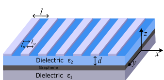
II Plasmons in a graphene-based SSH-like grating
In this system, experimentally studied in Ref. 41, we have a graphene sheet sandwiched between two dielectrics, characterized by dielectric constants and . On the upper-most dielectric, at a distance from the graphene sheet, there is a metal grating. The grating is a one-dimensional (1D) periodic structure composed of two alternating portions: a metallic section of length (denominated gated region) and an empty portion of length (named ungated region), such that the unit cell of length can be defined. The presence of a conductor significantly alters the properties of plasmons on graphene. For instance, the wavevectors of the gated ( and ungated regions differ, being given by [44]
| (1a) | |||
| (1b) |
respectively, where is the Fermi energy of graphene (considered to be equal in both regions), is the fine-structure constant, is the speed of light in vacuum, and is the plasmon frequency. We note that Eqs. (1a) and (1b) are analytical approximations to the exact dispersion, which can be known only numerically. To obtain them, it is necessary to assume that (i) the frequency regime is such that the conductivity of graphene is dominated by its Drude conductivity , (ii) absorption is zero (, and (iii) we can approximate the electrostatic limit, , where is the index labeling the dielectrics. Also, we consider values of such that , which has been considered in previous experiments [48]. The calculations leading to Eqs. (1a) and (1b) are detailed in Appendix A.
Our goal in this section is to use the transfer-matrix formalism to understand the propagation of graphene surface plasmons and to obtain the energy dispersion, associating the Bloch momentum , arising from the periodic arrangement of the metal grating, with the energy .
II.1 Fields, boundary conditions and transfer matrices
We begin by defining the expressions of the electrostatic potential describing propagating plasmons in the ungated and gated regions
| (2a) | |||
| (2b) |
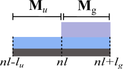
where the superscript correspond to the wave component traveling to the right (left). We can think of the gated regions as rectangular barriers of length that begin at and end at , and of ungated regions, that begin at and end at , where (for details see Fig. 2). We can then make use of appropriate boundary conditions to relate the electrostatic potential between gated and ungated regions. At the boundaries between regions we impose: (i) the continuity of the electrostatic potential and (ii) the continuity of the current density , where is the graphene conductivity (Drude conductivity) defined at the beginning of the section. At we have:
| (3a) | |||
| (3b) | |||
while at :
| (4a) | |||
| (4b) | |||
II.2 Dispersion and energy bands
Coefficients of the electrostatic potential across one period of the structure, at and , can be related by combining Eqs. (6a) and (6b). Consequently, we must then have:
| (7) |
The matrix is the unit cell transfer matrix, which is unitary, i.e., . The Bloch momentum is introduced by invoking Bloch’s theorem:
| (8) |
Non-trivial solutions of the system of Eqs. (7) and (8) for the coefficients are obtained if the determinant vanishes, i.e.,
| (9) |
where is the identity matrix. After taking into account the property of unitary matrices, Eq. (9) can be represented as [49]
| (10) |
This condition yields a Kronig–Penney-like dispersion relation for the graphene plasmons which, after taking the explicit form of matrices and into account, can be written in the form
| (11) |
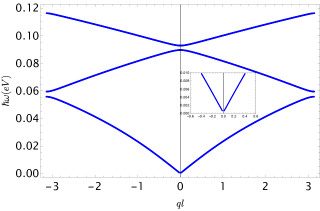
where . The numerical solution of the dispersion relation (11) is shown in Fig. 3. The periodicity of the structure results in a spectrum that consists in energy bands (where propagation of waves is allowed) and forbidden gaps (where the propagation is exponentially suppressed). Notice that in the low-frequency region the dispersion is linear (as shown in inset of Fig. 3). In this regime, we can expand Eq. (11) into a series with respect to the frequency , obtaining the following approximation
| (12) |
II.3 Propagation of graphene plasmons
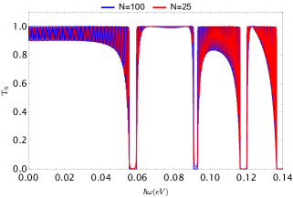
With both and , we have all necessary tools to describe the propagation of the graphene plasmon polaritons through the system. The transmission coefficient for a system with identical unit cells is given by [49]
| (13) |
where is the transfer matrix of the system with unit cells, which is the product of matrices . The element is given by Chebyshev’s identity [49] as:
| (14) |
The quantity is a phase related to the Bloch momentum and obeys Eq. (10). Thus, is easily obtainable after multiplying and the computation of yields:
| (15) | ||||
In Fig. 4 we represent the transmission coefficient as a function of the energy for and unit cells. As it can be seen from Fig. 4, for the frequency ranges corresponding to the gaps in the spectrum (see Fig. 3), transmittance turns to be zero, i.e., . Energy regions with zero transmittance correspond to the condition , as it follows from Eq. (10). For these frequencies the periodic structure serves as a plasmonic Bragg mirror. At the same time, for the frequency ranges corresponding to allowed bands in the spectrum, the nonzero transmittance exhibits periodical oscillations. Moreover, for frequencies corresponding to Bloch wavevector , where , the system becomes fully transparent and .
III Plasmonic SSH tight-binding model
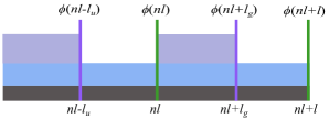
The goal in this section is to represent the electrostatic potential describing the plasmons in the tight-binding formalism. This representation is rather useful for the discussion of the topological description of the bands. The symmetry of the problem (absence of inversion symmetry and two segments composing one unit cell) invites us to make an analogy with a system that possesses sub-lattice symmetry, like the SSH model. To do this, we need to define the two sub-lattices: the first one is defined by the points at , depicted in purple in Fig. 5 and is associated with the end of gated regions. The other sub-lattice is defined by points at , depicted in green, and is associated with the end of ungated regions. To derive the tight-binding representation we then need to find expressions for the fields , , , and at each lattice site as a function of the previous and the next sites using the transfer-matrix formalism. For example, we want to obtain and , where , , and are the tight-binding coefficients to be determined.
III.1 Energy-dependent hopping amplitudes
The detailed derivation of the tight-binding equations can be found in Appendix B, where we show how to write the following equations relating lattice sites from two different sub-lattices:
| (16a) | |||
| (16b) |
These equations relate the electrostatic potential in one sub-lattice with the electrostatic potential at nearest-neighbor lattice points, contained in the other sub-lattice. The functions multiplying the electrostatic potentials play the role of hopping amplitudes in electronic tight-binding equations. To make Eqs. (16a) and (16b) look more similar to the SSH tight-binding Hamiltonian, we introduce
| (17a) | |||||
| (17b) | |||||
| (17c) | |||||
| (17d) | |||||
| (17e) | |||||
which conveniently allows us to rewrite Eqs. (16a) and (16b) as:
| (18a) | |||
| (18b) | |||
These coefficients are energy dependent through , , , and , and in this regard they differ from the usual SSH model where , , and C are constants. In order to vary these coefficients, it is then necessary to vary the gate tension applied to the metallic rods. Bloch’s theorem allows us to write and . In matrix notation, Eq. (18) then becomes:
| (19) |
The matrix with the coefficients and can be written as a linear combination of the Pauli matrices and , as usual in these type of problems [47]. That is, we can write
| (20) |
The coefficient , playing the role of the eigenvalue on the SSH model, has the form
| (21) |
where the explicit dependencies of the coefficients on , , and are kept as arguments of , , and . The two possible solutions of correspond to two separate bands when plotted against . This allows us to make a parallel with the original SSH [47], in which plays the role of the SSH model’s energy and Eq. (20) plays the role of the Hamiltonian. We make use of this parallelism to study the topological features of the plasmonic SSH.
III.2 Topological characterization in momentum space
In this section, we investigate the topology of our plasmonic SSH model, focusing our attention on the behavior of the first plasmonic energy gap, alongside the coefficient . We note that when there is a gap in the energy bands, there is also a gap in the plot versus . As we vary the distance from the metal we note that, as the first band gap closes, the gap in also closes at . This is exactly what happens in the electronic SSH model, but with the energy instead of [47]. We then expect that, if is the distance from the metal that closes the energy gap and the gap in , values of greater and smaller than will correspond to different topological phases. It is then necessary to find an analytical expression for , as we show next for the first energy band gap. Since both bands of touch at when the first energy gap closes, we can rewrite Eq. (21) as
| (22) |
Then it is clear that, for this condition to hold, . By taking the explicit form of the coefficients as in Eq. (17) into consideration, the conditions and can be rewritten as:
| (23a) | |||
| (23b) |
From Eq. (23a), we see that the cosines are equal but with opposite signs
| (24) |
The sine terms and are then either identical or have the same modulus but opposite sign as well. From Eq. (23b), we see that the sines must have the same sign, since and are strictly positive quantities and, to fulfill condition (23b), they should satisfy
| (25) |
Angles that have the same sine and opposite cosine sum to an odd multiple of :
| (26) |
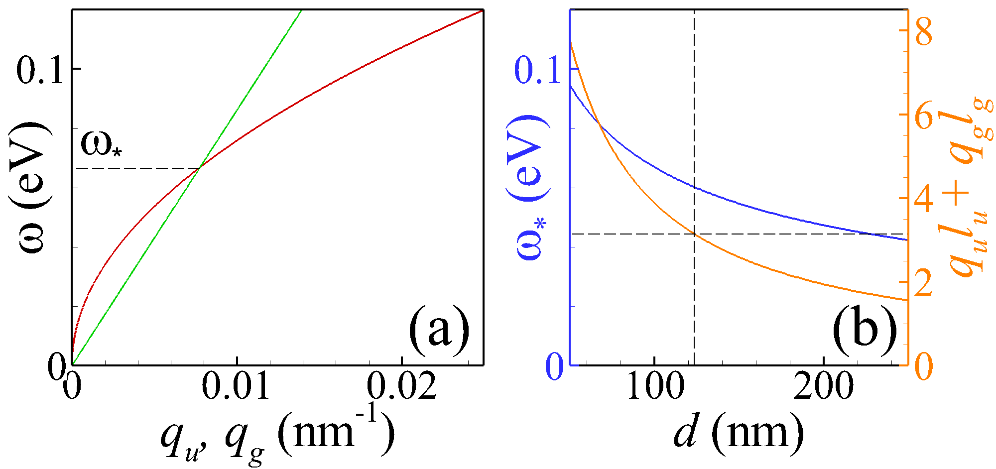
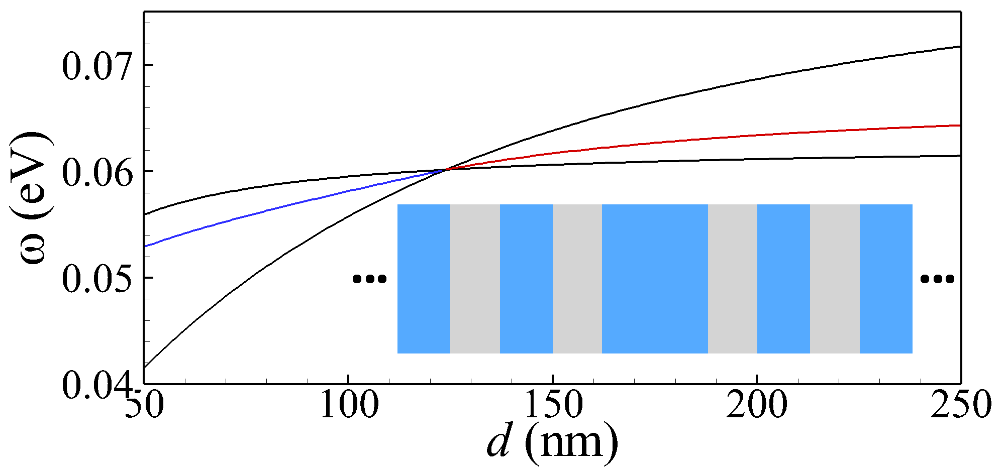
Now, from Eqs. (25) and (26) we can derive an analytical expression for the distance from the metal that makes the two bands of touch. This is straightforward if the explicit expressions for and are considered, given by Eqs. (1a) and (1b). Thus, for equal conductivities , condition (25) transforms into , which is fulfilled for a certain frequency (such that is the energy at the point where the two bands touch) [see Fig. 6(a)]. By combining Eqs. (1a) and (1b), an expression for frequency can be determined
| (27) |
This frequency varies with thickness as , as it is shown in Fig. 6(b) by the blue line (left axis). At the same time, condition (26) is fulfilled for and for critical thickness as expected [crossing of orange line in Fig. 6(b) with horizontal dashed line]. Substituting Eqs. (1a) and (1b) for frequency into condition (26), we obtain an equation for the critical thickness in the form
| (28) |
from which we obtain
| (29) |
This expression for is valid for all odd band gaps. By substituting the critical distance given by Eq. (29) into Eq. (27), we find the energies for which the odd band gaps close as only a function of and the parameters of the system. We observe that if , we have the value of at which the first band gap closes and, if , we have the value of at which the third band gap closes, and so on. At the end, we see that plays the role of the band gap index. We would like to point out that this formalism also applies to those band gaps that close at , like the second and fourth ones. The only difference is that, for this case, the cosines are equal in sign and modulus, while the sines have equal modulus but opposite sign. We would arrive at the conclusion that sum to an even multiple of , obeying with . Thus, Eq. (29) applies to all band gaps if we redefine .
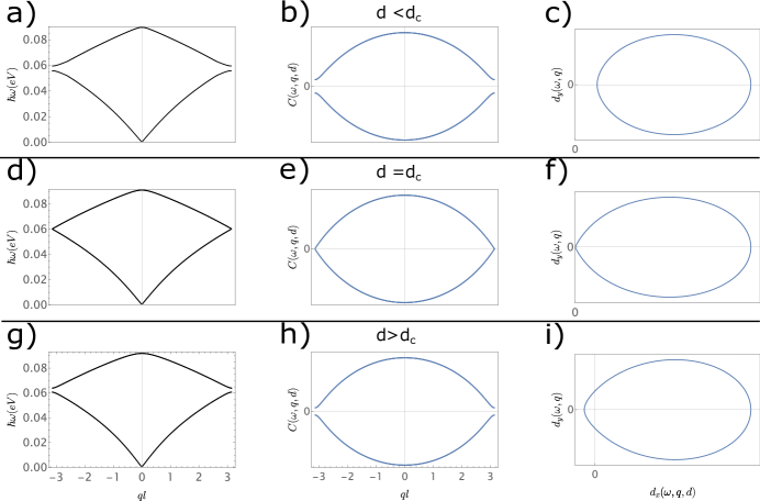
With the value of at hand, the remaining task is to identify which topological phase corresponds to and which corresponds to for the first energy band. This information can be obtained with the functions and as defined in Eq. (20). From the electronic SSH model [47] we know that, as varies from to , these functions describe a curve in the plane. This curve contains all information we need to state on which topological phase the system is in: if the curve winds around the origin, the system is said to be in the topological phase; if the curve does not wind around the origin, the system is said to be in the trivial phase; if the curve passes exactly through the origin, the system lies between topological phases and the energy band gap of the SSH model is closed. So, we expect that after choosing a value of and plotting and for the corresponding energies of the first energy band, as varies from to , we can find in which topological phase the system is in.
The results of this discussion are shown in Fig. 7. The first row corresponds to , the second row to and the third row to . In the first column, the first two energy bands are depicted. In the second column, the coefficient is plotted against . In the third column, we plot the parametric curve in the plane. Initially, looking at only the energy bands and the coefficient , it is not possible to distinguish between topological phases. However, the curve in the third column for does not wind around the origin, while the curve for does. This indicates that the first band has trivial topology for and non-trivial topology for . In the second row, we use to show that indeed the energy gap and the gap close simultaneously. Additionally, the corresponding curve passes exactly at the origin.
III.3 Defect states
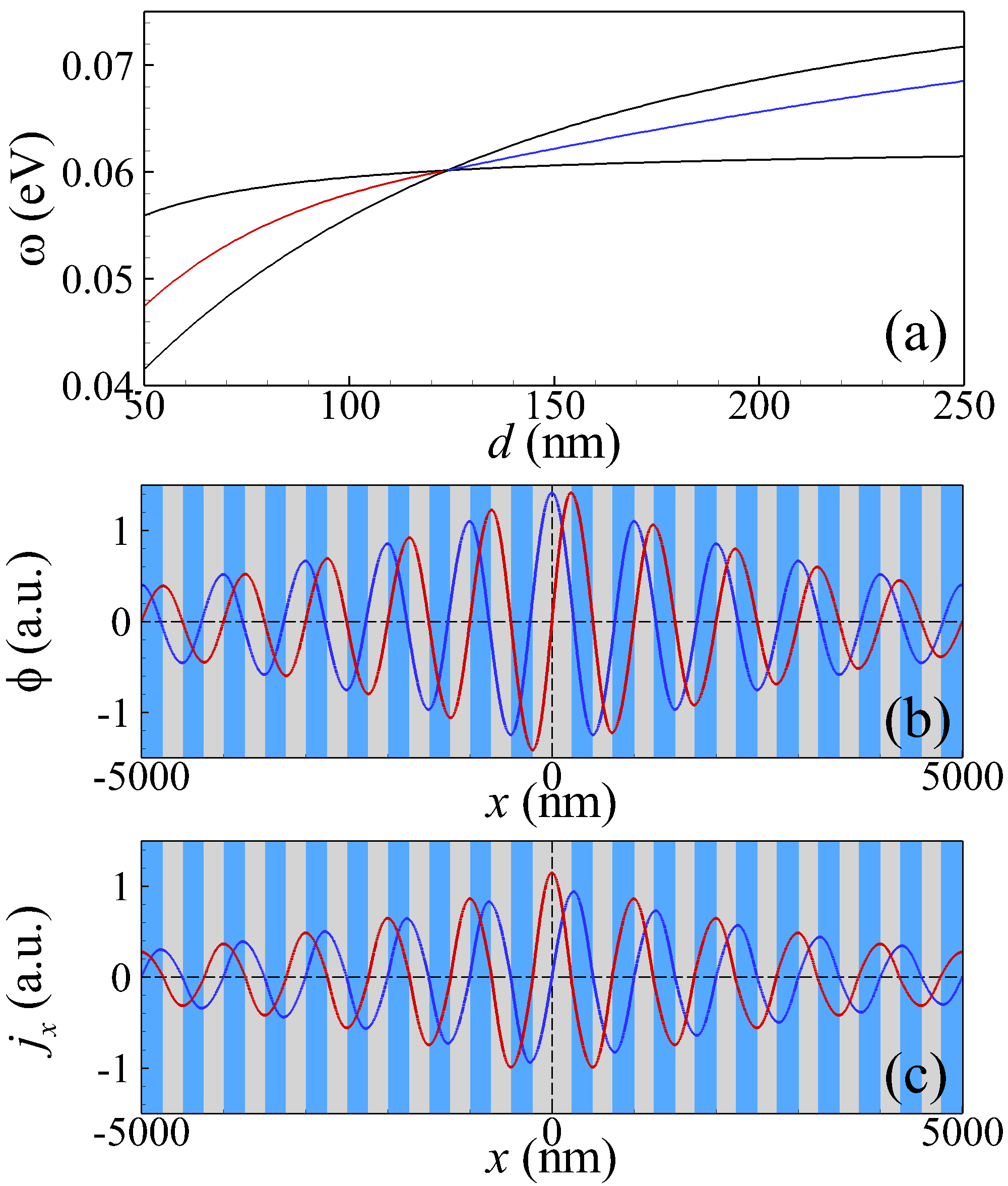
One of the advantages of characterization of structures by their topological properties is the ability to predict the existence of surface and defect states. In this subsection, we consider periodical structures with defects, which give rise to the presence of localized states. In Fig. 8 we show the spectrum of defect states in the structure, obtained from the periodic plasmonic crystal (considered in previous sections) by increasing twice the length of one of the gated regions. The presence of a single defect in the structure allows for the existence of localized defect states of two types: even and odd, whose spectra are shown in Fig. 8(a) by blue and red lines, respectively. Both defect states appear inside the first gap of the energy spectrum of the periodical structure [whose edges are depicted by black lines in Fig. 8(a)]. Even defect states exist for , for which the first band is characterized by non-trivial topology, while odd defect states exist for , for which the first band has trivial topology. Also, the spatial distribution of an even defect state is characterized by a reflective symmetry of the scalar potential and reflective anti-symmetry of the current density with respect to the symmetry plane [blue lines in Figs. 8(b) and 8(c)]. On the contrary, the spatial distribution of an odd defect state [red lines in Figs. 8(b) and 8(c)] is characterized by a reflective anti-symmetry of the scalar potential and reflective symmetry of the current density . The existence of defect states is also possible in a different version of structure, where one of the ungated regions has twice its usual length instead [see inset in Fig. 9]. As it can be seen from Fig. 9, the situation is reversed: even defect states (depicted by blue line) exist in the gap for , while odd defect states (depicted by red line) exist when . Thus, we have the opposite situation if we compare it to the case with a defect in the central gated region [compare with Fig. 8(a)], where even and odd states exist for and , respectively.
III.4 Analytical approximation for Dirac bands
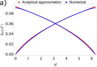
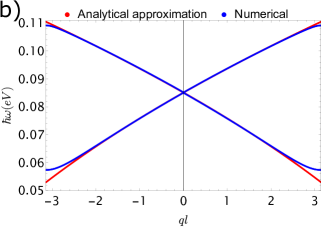
Another interesting aspect of the plasmonic SSH model is the fact that, when the energy gaps close, we obtain Dirac cones. It is possible to obtain an analytical approximations for the bands by inspecting the relationship between coefficients and . As stated in the previous section, for odd band gaps we have
| (30) |
meaning that . This is also true for even band gaps, since in these cases the conditions are
| (31) |
Thus, the relationship is always true, given that are evaluated at the energy where the bands touch and at . In this scenario, we can alter the form of the Kronig–Penney-like dispersion found for the graphene plasmons in Eq. (11) by substituting
| (32) |
The general solution to this equation has the form
| (33) |
where and the explicit expressions for and were used. Solving the quadratic equation for and preserving only the solutions corresponding to positive energies we arrive at
| (34) |
Again, we emphasize that = 1 only at the point where the bands touch and thus Eq. (34) is only an approximation. At the vicinity of the first gap (which is closed in this case) we use an expression for the critical thickness (29) for , as well as define Block wavevector in the limits . In this situation, two branches of frequencies can be obtained from Eq. (34) as
| (35) | |||
| (36) |
At the vicinity of the second gap, the expression for the critical thickness (29) should be used with , and the wavevector is defined inside the limits . In this case, Eq. (34) for the two branches of frequencies can be rewritten as
| (37) |
Close to the Dirac points, the square root in the expression above can be Taylor expanded such that the relationship between and is linear. For the first Dirac point, Eqs. (35) and (36) in the vicinity of will be represented as
| (38) |
For the second Dirac point, Eq. (37) in the vicinity of can be expanded as
| (39) |
In Fig. 10 we superpose the numerical calculations and the analytical approximation for the first and second energy band gaps. As expected, the result in Eq. (34) is better suited for around the Dirac points.
IV Conclusions
In this work we investigated a graphene-based polaritonic crystal. We showed that the plasmon energies obey a Kronig–Penney dispersion and calculated their propagation on the crystal with the transfer-matrix formalism. Upon realization that the crystal possesses sub-lattice symmetry, we managed to derive tight-binding equations for the electrostatic potential describing the plasmons. At the end, these equations resemble the SSH model tight-binding, one difference being that the hopping amplitudes are energy dependent. This representation is convenient because it allows us to bring the traditional formalism used to describe topological insulators in one dimension to plasmonics. By investigating the energy dispersion and the tight-binding coefficients we demonstrate that, by tuning the distance between graphene and the metal grating, it is possible to associate trivial and non-trivial topology to the energy bands of the polaritonic crystal. Additionally, we derived an analytical expression for , the value of that closes the energy band gaps. This expression can be used alongside numerical methods to easily identify the boundary between topological phases and to simplify the calculations involving the energy-dependent hopping amplitudes. Lastly, an analytical approximation for the energy bands was obtained by slightly modifying the Kronig–Penney-like dispersion. We show that this approximation describes the energy bands well if the energy gaps are closed, specially around Dirac points. We believe the findings of our work have the potential to facilitate future studies on topological plasmonics and provide a reliable framework to investigate similar polaritonic crystals analytically.
Acknowledgements
D. A. M. acknowledges the project PTDC/FIS-MAC/2045/2021 for a research grant. The Center for Polariton-driven Light–Matter Interactions (POLIMA) is funded by the Danish National Research Foundation (Project No. DNRF165). N. M. R. P. acknowledges support by the Portuguese Foundation for Science and Technology (FCT) in the framework of the Strategic Funding UIDB/04650/2020, COMPETE 2020, PORTUGAL 2020, FEDER, and through project PTDC/FIS-MAC/2045/2021. N. M. R. P. also acknowledges the Independent Research Fund Denmark (grant no. 2032-00045B) and the Danish National Research Foundation (Project No. DNRF165).
Appendix A Approximations for gated and ungated momenta
In the non-retarded (electrostatic) limit electromagnetic fields in graphene and surrounding media are defined by Poisson equation
| (40) |
where is the scalar potential,
| (41) |
is the dielectric permeability, and is the two-dimensional charge density in graphene. In the right-hand part of Eq. (40), the delta-function describes the fact that charges in graphene are concentrated on a two-dimensional plane, arranged at . Beyond the graphene plane, the Poisson equation can be solved separately in the spatial domains and , where the dielectric permeabilities are homogeneous, and the solution will have the form
| (42) |
Here the scalar potential is continuous at , and chose of signs in the exponential terms, containing guarantees that the surface wave is evanescent in the direction, and decays with increasing distance from the graphene plane at . Also solution (42) implies that surface plasmons propagate along the -axis with the wavevector and is oscillating in time with frequency .
If the Poisson equation (40) is integrated along -coordinate in the limits , it transforms into
| (43) |
Substituting Eq. (42) into Eq. (43), we obtain
| (44) |
The correspondent two-dimensional charge density can be obtained from the continuity equation
| (45) |
where three-dimensional current j in our particular case possesses only -component
| (46) |
where is the Drude 2D conductivity of graphene, the dominant conductivity term from THz to mid-IR [44]. Here and stand for the Fermi energy and inverse scattering time, respectively. In this paper we consider the case, where losses in graphene are absent (). Substituting current density from Eq. (46) into the continuity equation (45) and integrating it in time, we obtain the 2D charge density
| (47) |
This equation, being substituted into Eq. (43), gives the dispersion relation for ungated plasmons
| (48) |
If metal is present at a distance , the scalar potential turns put to be more complicated
| (52) |
In this case the 2D charge density will be the same as that in Eq. (47) [except should be substituted by ]. Substitution of the 2D charge density and the particular solution of Poisson equation (52) into Eq. (43) results in the dispersion relation for gated plasmons
| (53) |
For small distances between graphene and metal, , and . In this case the dispersion relation for gated plasmons can be expressed as
| (54) |
Appendix B Derivation of energy-dependent hopping amplitudes
B.1 Transfer matrix
We begin by determining the general transfer matrix relating, in one specific region labeled by , the functions at and :
| (55) |
where and is the corresponding transfer matrix in the region labeled by . The transfer-matrix coefficients can be found by expanding the expression above, using the definitions of in Eq. (2b):
| (56) |
Rearranging terms related to the same coefficients:
| (57) |
The exponentials of must then obey:
| (58) |
Expanding the exponentials into cosine and sine and solving the system of equations, it follows that for arbitrary the transfer-matrix coefficients are:
| (59) |
B.2 as a function of :
For the gated region in the unit cell we define:
| (60) |
| (61) |
Using the first row of the transfer matrix, Eq. (60) leads to
| (62) |
which can be rearranged as
| (63) |
Using the second row of Eq. (61) leads to:
| (64) |
which can be substituted into Eq. (63). After some manipulation and using trigonometric identities, this yields:
| (65) |
B.3 as a function of :
For the ungated region in the th unit cell we define:
| (66) |
| (67) |
This situation is exactly like the one for the gated region, but with the changes
With these substitutions, we find
| (68) |
B.4 The tight-binding equation
With Eqs. (65) and (68) we managed to write, for a given region, a function describing the plasmon in an arbitrary position in terms of functions at the boundaries. Now, we equate both Eqs. (65) and (68) at and to obtain the tight-binding equations (remember that the indexes and are irrelevant on the wavefunctions now): At (note that at this point, is evaluated in the th unit cell while is evaluated at the th unit cell):
| (69) |
| (70) |
| (71) |
At :
| (72) |
| (73) |
References
- Polman and Atwater [2005] A. Polman and H. A. Atwater, Materials Today 8, 56 (2005).
- Perenboom, Wyder, and Meier [1981] J. A. A. J. Perenboom, P. Wyder, and F. Meier, Physics Reports 78, 173 (1981).
- Bashevoy et al. [2006] M. V. Bashevoy, F. Jonsson, A. V. Krasavin, N. I. Zheludev, Y. Chen, and M. I. Stockman, Nano Letters 6, 1113 (2006).
- Mie [1908] G. Mie, Annalen der Physik 330, 377 (1908).
- Fan, Zheng, and Singh [2014] X. Fan, W. Zheng, and D. J. Singh, Light: Science Applications 3, e179 (2014).
- Khurgin [2015] J. B. Khurgin, Nature Nanotechnology 10, 2 (2015).
- Zeng et al. [2014] S. Zeng, D. Baillargeat, H.-P. Ho, and K.-T. Yong, Chemical Society Reviews 43, 3426 (2014).
- Yu et al. [2019] H. Yu, Y. Peng, Y. Yang, and Z.-Y. Li, npj Computational Materials 5, 45 (2019).
- Gadelha et al. [2021] A. C. Gadelha, D. A. Ohlberg, C. Rabelo, E. G. Neto, T. L. Vasconcelos, J. L. Campos, J. S. Lemos, V. Ornelas, D. Miranda, R. Nadas, F. C. Santana, K. Watanabe, T. Taniguchi, B. van Troeye, M. Lamparski, V. Meunier, V.-H. Nguyen, D. Paszko, J.-C. Charlier, L. C. Campos, L. G. Cançado, G. Medeiros-Ribeiro, and A. Jorio, Nature 590, 405 (2021).
- Jablan, Buljan, and Soljačić [2009] M. Jablan, H. Buljan, and M. Soljačić, Phys. Rev. B 80, 245435 (2009).
- Grigorenko, Polini, and Novoselov [2012] A. N. Grigorenko, M. Polini, and K. S. Novoselov, Nature Photonics 6, 749 (2012).
- Ni et al. [2018] G. Ni, A. McLeod, Z. Sun, L. Wang, L. Xiong, K. W. Post, S. S. Sunku, B.-Y. Jiang, J. Hone, C. R. Dean, M. M. Fogler, and D. N. Basov, Nature 557, 530 (2018).
- Fei et al. [2012] Z. Fei, A. S. Rodin, G. O. Andreev, W. Bao, A. S. McLeod, M. Wagner, L. M. Zhang, Z. Zhao, M. Thiemens, G. Dominguez, M. M. Fogler, A. H. Castro Neto, C. N. Lau, F. Keilmann, and D. N. Basov, Nature 487, 82–85 (2012).
- Woessner et al. [2015] A. Woessner, M. B. Lundeberg, Y. Gao, A. Principi, P. Alonso-González, M. Carrega, K. Watanabe, T. Taniguchi, G. Vignale, M. Polini, J. Hone, R. Hillenbrand, and F. H. L. Koppens, Nature Materials 14, 421 (2015).
- Brar et al. [2013] V. W. Brar, M. S. Jang, M. Sherrott, J. J. Lopez, and H. A. Atwater, Nano Letters 13, 2541 (2013).
- Koppens, Chang, and García de Abajo [2011] F. H. L. Koppens, D. E. Chang, and F. J. García de Abajo, Nano Letters 11, 3370 (2011).
- Rodrigo et al. [2015] D. Rodrigo, O. Limaj, D. Janner, D. Etezadi, F. J. García de Abajo, V. Pruneri, and H. Altug, Science 349, 165 (2015).
- Vasić, Isić, and Gajić [2013] B. Vasić, G. Isić, and R. Gajić, Journal of Applied Physics 113, 013110 (2013).
- Li et al. [2014] Y. Li, H. Yan, D. B. Farmer, X. Meng, W. Zhu, R. M. Osgood, T. F. Heinz, and P. Avouris, Nano Letters 14, 1573 (2014).
- Dai et al. [2020] Y. Dai, Z. Zhou, A. Ghosh, R. S. K. Mong, A. Kubo, C.-B. Huang, and H. Petek, Nature 588, 616 (2020).
- Gong et al. [2021] Y. Gong, L. Guo, S. Wong, A. J. Bennett, and S. S. Oh, Scientific Reports 11, 1055 (2021).
- Kim and Rho [2020] M. Kim and J. Rho, Nanophotonics 9, 3227 (2020).
- Süsstrunk and Huber [2015] R. Süsstrunk and S. D. Huber, Science 349, 47 (2015).
- Nash et al. [2015] L. M. Nash, D. Kleckner, A. Read, V. Vitelli, A. M. Turner, and W. T. M. Irvine, Proceedings of the National Academy of Sciences 112, 14495 (2015).
- Vila, Pal, and Ruzzene [2017] J. Vila, R. K. Pal, and M. Ruzzene, Physical Review B 96, 134307 (2017).
- Chen et al. [2018] H. Chen, H. Nassar, A. N. Norris, G. K. Hu, and G. L. Huang, Physical Review B 98, 094302 (2018).
- Shi et al. [2021] X. Shi, I. Kiorpelidis, R. Chaunsali, V. Achilleos, G. Theocharis, and J. Yang, Physical Review Research 3, 033012 (2021).
- Zhang et al. [2018] D.-W. Zhang, Y.-Q. Zhu, Y. X. Zhao, H. Yan, and S.-L. Zhu, Advances in Physics 67, 253 (2018).
- Wintersperger et al. [2020] K. Wintersperger, C. Braun, F. N. Ünal, A. Eckardt, M. D. Liberto, N. Goldman, I. Bloch, and M. Aidelsburger, Nature Physics 16, 1058 (2020).
- Konig et al. [2007] M. Konig, S. Wiedmann, C. Brune, A. Roth, H. Buhmann, L. W. Molenkamp, X.-L. Qi, and S.-C. Zhang, Science 318, 766 (2007).
- Fu, Kane, and Mele [2007] L. Fu, C. L. Kane, and E. J. Mele, Physical Review Letters 98, 106803 (2007).
- Chen et al. [2009] Y. L. Chen, J. G. Analytis, J.-H. Chu, Z. K. Liu, S.-K. Mo, X. L. Qi, H. J. Zhang, D. H. Lu, X. Dai, Z. Fang, S. C. Zhang, I. R. Fisher, Z. Hussain, and Z.-X. Shen, Science 325, 178 (2009).
- Su, Schrieffer, and Heeger [1979] W. P. Su, J. R. Schrieffer, and A. J. Heeger, Physical Review Letters 42, 1698 (1979).
- Zhang et al. [2023] L. Zhang, X.-M. Wang, X.-M. Qiu, Z. Wang, and J.-Y. Yan, Physical Review B 108, 085402 (2023).
- Jin et al. [2017] D. Jin, T. Christensen, M. Soljačić, N. X. Fang, L. Lu, and X. Zhang, Physical Review Letters 118, 245301 (2017).
- Ju et al. [2011] L. Ju, B. Geng, J. Horng, C. Girit, M. Martin, Z. Hao, H. A. Bechtel, X. Liang, A. Zettl, and F. Wang, Nature Nanotechnology 6, 630 (2011).
- Nikitin et al. [2012] A. Y. Nikitin, F. Guinea, F. J. Garcia-Vidal, and L. Martin-Moreno, Physical Review B 85, 081405(R) (2012).
- Strait et al. [2013] J. H. Strait, P. Nene, W.-M. Chan, C. Manolatou, S. Tiwari, F. Rana, J. W. Kevek, and P. L. McEuen, Physical Review B 87, 241410(R) (2013).
- Zhao and Zhang [2015] B. Zhao and Z. M. Zhang, ACS Photonics 2, 1611 (2015).
- Dias and Peres [2017] E. J. C. Dias and N. M. R. Peres, ACS Photonics 4, 3071 (2017).
- Bylinkin et al. [2019] A. Bylinkin, E. Titova, V. Mikheev, E. Zhukova, S. Zhukov, M. Belyanchikov, M. Kashchenko, A. Miakonkikh, and D. Svintsov, Physical Review Applied 11, 054017 (2019).
- Rappoport et al. [2021] T. G. Rappoport, Y. V. Bludov, F. H. L. Koppens, and N. M. R. Peres, ACS Photonics 8, 1817 (2021).
- Guo and Argyropoulos [2023] T. Guo and C. Argyropoulos, Journal of Applied Physics 134, 050901 (2023).
- Gonçalves and Peres [2016] P. A. D. Gonçalves and N. M. R. Peres, An Introduction To Graphene Plasmonics (World Scientific Publishing Company, 2016).
- Menabde et al. [2022] S. G. Menabde, J. T. Heiden, J. D. Cox, N. A. Mortensen, and M. S. Jang, Nanophotonics 11, 2433 (2022).
- Kronig and Penney [1931] R. D. L. Kronig and W. G. Penney, Proceedings of the Royal Society of London A 130, 499 (1931).
- Asbóth, Oroszlány, and Pályi [2016] J. Asbóth, L. Oroszlány, and A. Pályi, A Short Course on Topological Insulators: Band Structure and Edge States in One and Two Dimensions, Lecture Notes in Physics (Springer, 2016).
- Iranzo et al. [2018] D. A. Iranzo, S. Nanot, E. J. C. Dias, I. Epstein, C. Peng, D. K. Efetov, M. B. Lundeberg, R. Parret, J. Osmond, J.-Y. Hong, J. Kong, D. R. Englund, N. M. R. Peres, and F. H. L. Koppens, Science 360, 291 (2018).
- Markos and Soukoulis [2008] P. Markos and C. Soukoulis, Wave Propagation: From Electrons to Photonic Crystals and Left-Handed Materials (Princeton University Press, 2008).