Tunable coupling of a quantum phononic resonator to a transmon qubit with flip-chip architecture
Abstract
A hybrid system with tunable coupling between phonons and qubits shows great potential for advancing quantum information processing. In this work, we demonstrate strong and tunable coupling between a surface acoustic wave (SAW) resonator and a transmon qubit based on galvanic-contact flip-chip technique. The coupling strength varies from 7.0 MHz to -20.6 MHz, which is extracted from different vacuum Rabi oscillation frequencies. The phonon-induced ac Stark shift of the qubit at different coupling strengths is also shown. Our approach offers a good experimental platform for exploring quantum acoustics and hybrid systems.
Circuit quantum acoustodynamics (cQAD) studies the interaction between mechanical vibrations and superconducting qubits, which provides a way to control the non-classical mechanical modes (phonons). There are various mechanical degrees of freedom including bulk wave Chu et al. (2017), surface acoustic wave (SAW) Gustafsson et al. (2014); Manenti et al. (2017); Bolgar et al. (2018); Moores et al. (2018); Satzinger et al. (2018); Kitzman et al. (2023) and vibrations of suspended beams O’Connell et al. (2010); Pirkkalainen et al. (2013); Wollack et al. (2022); Lee et al. (2023). Among them, SAW is a traveling acoustic wave that propagates on the surface of the solid materials. Confining SAW between the Bragg mirrors can form the Fabry-Perot SAW cavity with achieved quality factor (Q) up to Manenti et al. (2016a); Emser et al. (2022). Compared to circuit quantum electrodynamics (cQED) systems Blais et al. (2021); Gu et al. (2017), acoustic waves travel five orders of magnitude slower than electromagnetic waves and the wavelength of gigahertz acoustic waves is close to that of optical waves. Therefore, the cQAD system has various applications, such as phonon-mediated quantum state transfer Bienfait et al. (2019), quantum random access memory Hann et al. (2019) and medium for microwave-optical conversion Forsch et al. (2020); Mirhosseini et al. (2020); Han et al. (2021). Some impressive work has been done to study the physical properties of cQAD systems, including preparation of phonon Fock states Satzinger et al. (2018); Chu et al. (2018), splitting of phonons Sletten et al. (2019); Qiao et al. (2023), phonon induced non-exponential decay of giant atoms Andersson et al. (2019), electromagnetically induced acoustic transparency Andersson, Ekström, and Delsing (2020), squeezing and entanglement Wollack et al. (2022); Andersson et al. (2022) of phonon states.
For cQAD system, compared to weak coupling, strong coupling promises performing more coherent operations between superconducting qubits and other phononic resonators. Strong coupling regime can be achieved by improving the coherence time of the cQAD system or increasing the coupling strength. Fabricating the qubits directly on piezoelectric materials will induce phonon loss channel to the qubits. Therefore, it is better to fabricate the qubit and SAW on two different materials to keep good performance of cQAD system. There are two ways to realize the target. One way involves using piezoelectric films on sapphire substrate and placing the qubit on the area where the piezoeletric films are etched Jiang et al. (2023); Xu et al. (2022). However, etching could cause damages to the substrate surface. The other option is to utilize flip-chip architecture to assemble two substrates made of different materials Chu et al. (2017); Satzinger et al. (2018). The reported flip-chip technology Satzinger et al. (2018); Kitzman et al. (2023) used in the cQAD system relies on glue. Therefore, the coupling strength between the qubit and SAW cavity is determined by the interchip geometric capacitance or mutual inductance and the grounding plane could be affected by glue bumps.
Here, we report fabrication process and characterizations of the device which couples a GHz-frequency SAW resonator (cavity) to a transmon qubit. The qubit chip and SAW cavity chip are bounded together by flip-chip assembly with galvanic bumps (Indium). We verify the strong coupling between the SAW cavity and the qubit by performing vacuum Rabi oscillations experiment. Due to the existence of a tunable coupler, we can adjust the coupling strength in a range from 7.0 to MHz. Then we measure the ac Stark shift of the qubit to show the effect of phonons inside the SAW cavity on the qubit. Our galvanic-connected flip-chip device can be realized with stronger coupling strength while ensuring the coherence of each elements.
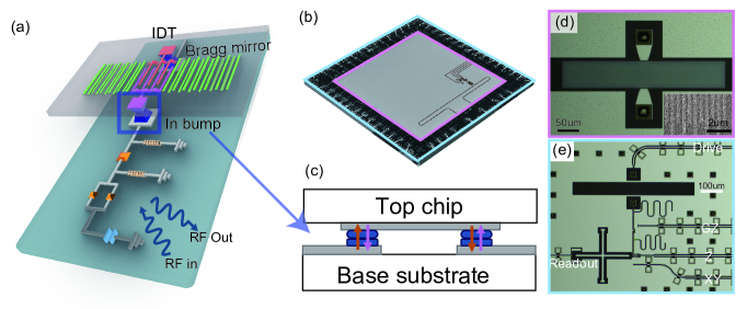
Our device, as shown in Fig. 1a, is composed of two chips, which are bonded together using flip-chip technology. The top chip consists of a SAW resonator, fabricated on Y-X lithium niobate () substrate – a kind of material with strong piezoelectric effect. The SAW cavity is formed by an IDT (purple and orange) and two Bragg mirrors (green) on both sides. The IDT can conduct the conversion between acoustic waves and microwave, as well as excitation and detection of SAWs. The Bragg mirrors use grattings to form a Fabry-Perot cavity Manenti et al. (2016b), which supports a stopband in the frequency responseMorgan (2007). The base substrate is sapphire and is used to fabricate qubits and control lines. The reason why we need two kinds of substrate is that the dielectric loss on is very large and will cause decoherence of qubits Ioffe et al. (2004). The artificial atom we use is a frequency- tunable transmon qubit, formed by a DC SQUID and a shunted capacitor. The transmon qubit connects to the SAW cavity through a RF SQUID (i.e. gmon Chen et al. (2014); Geller et al. (2015)) with tunable inductance and indium bumps, which provides galvanic contact between the top and base chips. Compared to the designs in Ref. Satzinger et al. (2018), we do not need to use interchip mutual inductance to make connection, which is sensitive to the space between the chips and has limited values. As show in Fig. 1e, the transmon qubit is controlled by XY lines with the rotation in X or Y axis in the Bloch sphere and Z lines which tunes the transition frequency of qubit by applied flux bias. The state of the transmon qubit is read out by the dispersive-coupling coplanar waveguide resonator.
The fabrication of the device uses electron beam lithography (EBL) and optic laser lithography. First, we use ebeam evaporation to deposit nm Al for the base chip and nm Al for the top chip, respectively. Then, we use optic lithography and wet etch to form coplanar waveguides (CPWs) and ground planes. The stripes of the SAW cavity in the top chip are defined through EBL with width as nm and length as um using photoresist PMMA. These slender stripes are extremely difficult to be fabricated, especially when the periodic cell number of the Bragg mirrors at each side is 400 and the periodic cell number of IDT is . Before the evaporation process, we conduct the oxygen plasma cleaning in situ to remove the resist residue using Plassys. The Al stripes are made by two steps. The first step is to create extra undercuts with the deposition angle at and nm Al, facilitating the lift-off process. The second step is to deposit nm Al at angle. This deposition method is also used in Ref. Bolgar et al. (2018). The stripe structrues after lift-off are shown in Fig. 1d. The qubits in the base chip are exposed with EBL and fabricated with standard Dolan bridge shadow evaporation. The final step is to make flip-chip architecture using FC150 bonder. Although indium is a commonly used metal for flip-chip bonding Datta (2010) and becomes superconductive below K, the direct contact between aluminum and indium will form an intermetallic Foxen et al. (2018); Wade and Banister (1975), damaging the conductivity of these bumps. To address this issue, we use niobium as the diffusion barrier, which can be deposited via magnetron sputtering and also exhibits superconductivity below K. Then, we deposit indium on each chips with the thickness of m using thermal evaporation. Note that we conduct ion mill in situ to make good electrical contact prior to each metal deposition. The two chips are bonded together with a force of g, ensuring the distance between them around m. The complete device is shown in Fig. 1b with the side-view diagram in Fig. 1c.
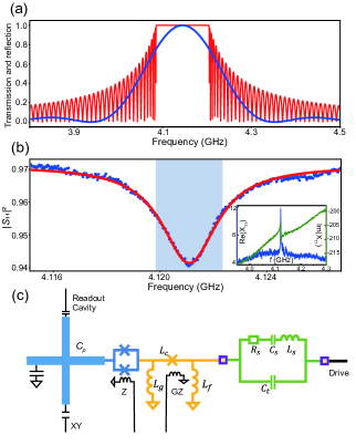
The frequency response of SAW cavity can be simulated with the coupling-of-mode (COM) model Morgan (2007). The propagation speed of SAW in Y-X is m/s at room temperature Shibayama et al. (1976). The periodicity of IDT stripes is and determines the central wavelength and frequency of the excited acoustic wave as and . Both overexposure in EBL and the placed direction of IDT will affect its central frequency because is an anisotropic material. The calculated conductance of IDT is a function at with the bandwidth MHz, as shown in Fig. 2a. The reflection of single electrode in the Bragg mirror is . We need to conduct the Bragg mirror with a stripe array, in order to improve the total reflection rate to 1 by using the interference among them. The bandwidth of Bragg mirror is MHz, which should be less than , and is used to select frequency and improve Q factor.
We show the measured reflection data of the SAW cavity with and the distance between the two Bragg mirrors in Fig. 2b. The equivalent inductance can be calculated with , where the reactance in the insert can be calculated from the measured data and . The calculated BVD parameters of the SAW cavity in in Fig. 2b are nH, fF and with the characteristic impedance and the room temperature Q factor . The electrostatic capacitance of IDT is fF.
To study the cQAD system in the quantum regime, we mount the sample inside the mixing chamber of a dilution refrigerator with base temperature around mk. The transmon qubit can be described by the charge energy GHz with fF and maximal Josephson energy GHz. The transition frequency from ground to first-excited state of the qubit can be turned by external flux as with . The Hamiltonian of the system shown in Fig. 2c can be described by Jaynes-Cummings model as
| (1) |
where is the annihilation operator of SAW cavity mode, () is the annihilation (creation) operator and is the population operator of the transmon qubit. is the resonance frequency of SAW cavity at low temperature. is the coupling strength between SAW cavity and qubit and is adjustable as
| (2) |
where is the tunable inductance of gmon and is the phase difference across the junction, tuned by the DC bias in the RF SQUID. The parameters of the gmon loop are pH, pH and pH, which are obtained by the measured coupling strengths (discussed later). is the inductance of the transmon qubit, which is around nH and can be tuned by the external flux.
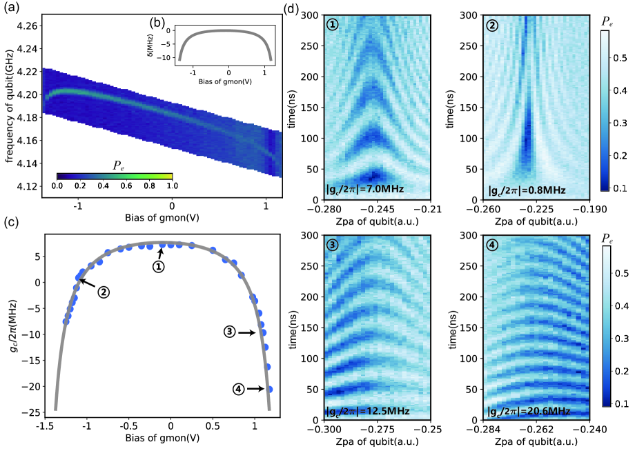
Figure 3a shows how the transition frequency of qubit is modulated by the bias of gmon. The applied voltage converts to biased current in the local control lines on chip because of the series resistors in the input lines. The effective inductance of gmon changes with the bias voltage and affects the transition frequency of qubit. Moreover, the applied voltage to gmon causes Z-crosstalk to the qubit. After correcting, the modulated curve is shown in Fig. 3b.
We prepare the qubit to excited state (denote ground and excited state of qubit as and , the Fock state of SAW cavity as , ) then track the time-domain response of the qubit over a narrow range around the frequency of SAW cavity by qubit fast Z-control pulse. As the qubit bias is moved to resonance with SAW cavity causing oscillation between dressed states and , we expect the beating frequency to decrease to as shown in Fig. 3d. The frequency of SAW cavity can be obtained as GHz. We conduct experiments under different gmon biases in Fig. 3c to investigate the variation of qubit-SAW cavity coupling strength with gmon bias. Fig. 3d➀-➃ presents the Rabi oscillations of different effective coupling strength obtained in our measurements, Fig. 3d➃ shows a maximum MHz.
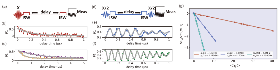
The pulse sequence for the measurement of the phonon’s energy relaxation time () in SAW cavity is depicted in Fig. 4a. The qubit is excited with X gate while off-resonance, and then coupled to the SAW cavity for ns to transfer the state with an iSWAP. A second iSWAP later retrieves the state back to qubit for readout. The resulting decay in Fig. 4b gives the lifetime of a single phonon in SAW cavity yields ns.
The entire relaxation process can be divided into three parts: the first iSWAP gate, the delay and the second iSWAP gate, as denoted in Fig. 4a. The dissipation experienced by the system during the swap process is contributed by both the qubit and the cavity, depending on their individual dissipation rates and , respectively. On the other hand, the qubit and SAW cavity are in a large detuning during the delay, introducing a Purcell effect for SAW cavity, where and is the dissipation rates of qubit at idle frequency. Two iSWAP gates only change the initial value of the curve so the population of SAW cavity being in the entire process is denoted as
| (3) |
According to the experimental parameters in Fig. 4b and Fig. 4d, the additional dissipation caused by the Purcell effect is much smaller than intrinsic dissipation, i.e. . Therefore, the we measured is reliable which allows the determination of the quality factor .The of SAW cavity can be measured by the pulse sequence shown in Fig. 4d which is similar to the case of . Figs. 4e and 4f show the measured data of SAW cavity and the qubit at the idle point, respectively.
Finally, we used the ac Stark effect to calibrate the phonon number in the SAW cavity. According to the results of c-QED in dispersive regime, the frequency of the qubit varies with the number of phonons in the cavity
| (4) |
Applying resonance driving with different powers to the SAW cavity and scanning the spectrum of qubit at the same time. According to MHz, we calibrated the average number of phonons by frequency shift of qubit as . We adjusted the gmon’s bias and measured the qubit frequency shift at different coupling strengths, as shown in Fig. 4g. According to Eq. 4, with the same and , the slope of versus the should be proportional to . This is consistent with our experimental results. It also reveals another method for measuring electro-acoustic coupling.
In summary, we integrate the SAW cavity and the transmon qubit together using flip-chip assembly with indium bumps. Using this cQAD device, we observe the strong coupling between the qubit and SAW cavity and show the tunability of the coupling strength. Furthermore, we observe the ac stark shift of the qubit causing by the phonons in the SAW cavity. Comparing the characterization of SAW cavity in room temperature, we observe an improvement in the Q factor under lower temperatures. These can be explained by the smaller acoustic dissipation of mK within the high-vacuum environment. Our work provides a new platform for studying cQAD and a new way to integrate them. The galvanic-connected flip-chip technology gives a modular way to optimize the qubit and mechnical modes separately. This new platform has potential applications in quantum communication and quantum computing.
Acknowledgements.
This work was supported by the National Natural Science Foundation of China (Grants No. 12204528, No. 92265207, No. T2121001, No. 11934018, No. 12005155, No. 11904393, No. 92065114, No. 12204528, No. 11875220, and No. 12047502), Innovation Program for Quantum Science and Technology (Grant No. 2021ZD0301800), and Scientific Instrument Developing Project of Chinese Academy of Sciences (Grant No. YJKYYQ20200041). Z.H. Peng also acknowledges the funding support by the National Natural Science Foundation of China (Grant No. 12074117, No. 92365209). J. Zhang also acknowledges the funding support by Tsinghua-Foshan Innovation Special Fund (TFISF), Innovative leading talent project of "Shuangqian plan" in Jiangxi Province, Joint Fund of Science and Technology Department of Liaoning Province and State Key Laboratory of Robotics, China (2021-KF-22-01) and Guoqiang Research Institute of Tsinghua University (20212000704). X.H. Ruan thanks for the measurement support from Xu Wang in CAS. This work also was supported by the Micro/nano Fabrication Laboratory of Synergetic Extreme Condition User Facility (SECUF). Devices were made at the Nanofabrication Facilities at the Institute of Physics, CAS in Beijing.AUTHOR DECLARATIONS
Conflict of Interest
The authors have no conflicts to disclose.
References
- Chu et al. (2017) Y. Chu, P. Kharel, W. H. Renninger, L. D. Burkhart, L. Frunzio, P. T. Rakich, and R. J. Schoelkopf, “Quantum acoustics with superconducting qubits,” Science 358, 199–202 (2017).
- Gustafsson et al. (2014) M. V. Gustafsson, T. Aref, A. F. Kockum, M. K. Ekström, G. Johansson, and P. Delsing, “Propagating phonons coupled to an artificial atom,” Science 346, 207–211 (2014).
- Manenti et al. (2017) R. Manenti, A. F. Kockum, A. Patterson, T. Behrle, J. Rahamim, G. Tancredi, F. Nori, and P. J. Leek, “Circuit quantum acoustodynamics with surface acoustic waves,” Nature Communications 8, 975 (2017).
- Bolgar et al. (2018) A. N. Bolgar, J. I. Zotova, D. D. Kirichenko, I. S. Besedin, A. V. Semenov, R. S. Shaikhaidarov, and O. V. Astafiev, “Quantum Regime of a Two-Dimensional Phonon Cavity,” Physical Review Letters 120, 223603 (2018).
- Moores et al. (2018) B. A. Moores, L. R. Sletten, J. J. Viennot, and K. W. Lehnert, “Cavity Quantum Acoustic Device in the Multimode Strong Coupling Regime,” Physical Review Letters 120, 227701 (2018).
- Satzinger et al. (2018) K. J. Satzinger, Y. P. Zhong, H.-S. Chang, G. A. Peairs, A. Bienfait, M.-H. Chou, A. Y. Cleland, C. R. Conner, E. Dumur, J. Grebel, I. Gutierrez, B. H. November, R. G. Povey, S. J. Whiteley, D. D. Awschalom, D. I. Schuster, and A. N. Cleland, “Quantum control of surface acoustic wave phonons,” Nature 563, 661–665 (2018).
- Kitzman et al. (2023) J. M. Kitzman, J. R. Lane, C. Undershute, P. M. Harrington, N. R. Beysengulov, C. A. Mikolas, K. W. Murch, and J. Pollanen, “Phononic bath engineering of a superconducting qubit,” Nature Communications 14, 3910 (2023).
- O’Connell et al. (2010) A. D. O’Connell, M. Hofheinz, M. Ansmann, R. C. Bialczak, M. Lenander, E. Lucero, M. Neeley, D. Sank, H. Wang, M. Weides, J. Wenner, J. M. Martinis, and A. N. Cleland, “Quantum ground state and single-phonon control of a mechanical resonator,” Nature 464, 697–703 (2010).
- Pirkkalainen et al. (2013) J.-M. Pirkkalainen, S. U. Cho, J. Li, G. S. Paraoanu, P. J. Hakonen, and M. A. Sillanpää, “Hybrid circuit cavity quantum electrodynamics with a micromechanical resonator,” Nature 494, 211–215 (2013).
- Wollack et al. (2022) E. A. Wollack, A. Y. Cleland, R. G. Gruenke, Z. Wang, P. Arrangoiz-Arriola, and A. H. Safavi-Naeini, “Quantum state preparation and tomography of entangled mechanical resonators,” Nature 604, 463–467 (2022).
- Lee et al. (2023) N. R. Lee, Y. Guo, A. Y. Cleland, E. A. Wollack, R. G. Gruenke, T. Makihara, Z. Wang, T. Rajabzadeh, W. Jiang, F. M. Mayor, P. Arrangoiz-Arriola, C. J. Sarabalis, and A. H. Safavi-Naeini, “Strong dispersive coupling between a mechanical resonator and a fluxonium superconducting qubit,” PRX Quantum 4, 040342 (2023).
- Manenti et al. (2016a) R. Manenti, M. J. Peterer, A. Nersisyan, E. B. Magnusson, A. Patterson, and P. J. Leek, “Surface acoustic wave resonators in the quantum regime,” Physical Review B 93, 041411 (2016a).
- Emser et al. (2022) A. L. Emser, B. C. Rose, L. R. Sletten, P. Aramburu Sanchez, and K. W. Lehnert, “Minimally diffracting quartz for ultra-low temperature surface acoustic wave resonators,” Applied Physics Letters 121, 224001 (2022).
- Blais et al. (2021) A. Blais, A. L. Grimsmo, S. M. Girvin, and A. Wallraff, “Circuit quantum electrodynamics,” Rev. Mod. Phys. 93, 025005 (2021).
- Gu et al. (2017) X. Gu, A. F. Kockum, A. Miranowicz, Y.-x. Liu, and F. Nori, “Microwave photonics with superconducting quantum circuits,” Physics Reports 718–719, 1–102 (2017).
- Bienfait et al. (2019) A. Bienfait, K. J. Satzinger, Y. P. Zhong, H.-S. Chang, M.-H. Chou, C. R. Conner, É. Dumur, J. Grebel, G. A. Peairs, R. G. Povey, and A. N. Cleland, “Phonon-mediated quantum state transfer and remote qubit entanglement,” Science 364, 368–371 (2019).
- Hann et al. (2019) C. T. Hann, C.-L. Zou, Y. Zhang, Y. Chu, R. J. Schoelkopf, S. M. Girvin, and L. Jiang, “Hardware-Efficient Quantum Random Access Memory with Hybrid Quantum Acoustic Systems,” Physical Review Letters 123, 250501 (2019).
- Forsch et al. (2020) M. Forsch, R. Stockill, A. Wallucks, I. Marinković, C. Gärtner, R. A. Norte, F. van Otten, A. Fiore, K. Srinivasan, and S. Gröblacher, “Microwave-to-optics conversion using a mechanical oscillator in its quantum ground state,” Nature Physics 16, 69–74 (2020).
- Mirhosseini et al. (2020) M. Mirhosseini, A. Sipahigil, M. Kalaee, and O. Painter, “Quantum transduction of optical photons from a superconducting qubit,” Nature 588, 599–603 (2020).
- Han et al. (2021) X. Han, W. Fu, C.-L. Zou, L. Jiang, and H. X. Tang, “Microwave-optical quantum frequency conversion,” Optica 8, 1050 (2021).
- Chu et al. (2018) Y. Chu, P. Kharel, T. Yoon, L. Frunzio, P. T. Rakich, and R. J. Schoelkopf, “Creation and control of multi-phonon Fock states in a bulk acoustic-wave resonator,” Nature 563, 666–670 (2018).
- Sletten et al. (2019) L. R. Sletten, B. A. Moores, J. J. Viennot, and K. W. Lehnert, “Resolving Phonon Fock States in a Multimode Cavity with a Double-Slit Qubit,” Physical Review X 9, 021056 (2019).
- Qiao et al. (2023) H. Qiao, É. Dumur, G. Andersson, H. Yan, M.-H. Chou, J. Grebel, C. R. Conner, Y. J. Joshi, J. M. Miller, R. G. Povey, X. Wu, and A. N. Cleland, “Splitting phonons: Building a platform for linear mechanical quantum computing,” Science 380, 1030–1033 (2023).
- Andersson et al. (2019) G. Andersson, B. Suri, L. Guo, T. Aref, and P. Delsing, “Non-exponential decay of a giant artificial atom,” Nature Physics 15, 1123–1127 (2019).
- Andersson, Ekström, and Delsing (2020) G. Andersson, M. K. Ekström, and P. Delsing, “Electromagnetically Induced Acoustic Transparency with a Superconducting Circuit,” Physical Review Letters 124, 240402 (2020).
- Andersson et al. (2022) G. Andersson, S. W. Jolin, M. Scigliuzzo, R. Borgani, M. O. Tholén, J. Rivera Hernández, V. Shumeiko, D. B. Haviland, and P. Delsing, “Squeezing and Multimode Entanglement of Surface Acoustic Wave Phonons,” PRX Quantum 3, 010312 (2022).
- Jiang et al. (2023) W. Jiang, J. Chen, X. Liu, Z. Niu, K. Liu, W. Peng, Z. Wang, and Z.-R. Lin, “Thin film aluminum nitride surface acoustic wave resonators for quantum acoustodynamics,” Applied Physics Letters 123, 024002 (2023).
- Xu et al. (2022) X.-B. Xu, J.-Q. Wang, Y.-H. Yang, W. Wang, Y.-L. Zhang, B.-Z. Wang, C.-H. Dong, L. Sun, G.-C. Guo, and C.-L. Zou, “High-frequency traveling-wave phononic cavity with sub-micron wavelength,” Applied Physics Letters 120, 163503 (2022).
- Manenti et al. (2016b) R. Manenti, M. J. Peterer, A. Nersisyan, E. B. Magnusson, A. Patterson, and P. J. Leek, “Surface acoustic wave resonators in the quantum regime,” Physical Review B 93, 041411 (2016b).
- Morgan (2007) D. Morgan, Surface Acoustic Wave Filters: With Applications to Electronic Communications and Signal Processing(second edition) (Academic Press, Oxford, 2007).
- Ioffe et al. (2004) L. B. Ioffe, V. B. Geshkenbein, C. Helm, and G. Blatter, “Decoherence in superconducting quantum bits by phonon radiation,” Physical Review Letters 93, 057001 (2004).
- Chen et al. (2014) Y. Chen, C. Neill, P. Roushan, N. Leung, M. Fang, R. Barends, J. Kelly, B. Campbell, Z. Chen, B. Chiaro, A. Dunsworth, E. Jeffrey, A. Megrant, J. Y. Mutus, P. J. J. O’Malley, C. M. Quintana, D. Sank, A. Vainsencher, J. Wenner, T. C. White, M. R. Geller, A. N. Cleland, and J. M. Martinis, “Qubit Architecture with High Coherence and Fast Tunable Coupling,” Physical Review Letters 113, 220502 (2014).
- Geller et al. (2015) M. R. Geller, E. Donate, Y. Chen, M. T. Fang, N. Leung, C. Neill, P. Roushan, and J. M. Martinis, “Tunable coupler for superconducting Xmon qubits: Perturbative nonlinear model,” Physical Review A 92, 012320 (2015).
- Datta (2010) M. Datta, “Microelectronic packaging trends and the role of nanotechnology,” in Electrochemical Nanotechnologies (Springer New York, New York, NY, 2010) pp. 227–253.
- Foxen et al. (2018) B. Foxen, J. Y. Mutus, E. Lucero, R. Graff, A. Megrant, Y. Chen, C. Quintana, B. Burkett, J. Kelly, E. Jeffrey, Y. Yang, A. Yu, K. Arya, R. Barends, Z. Chen, B. Chiaro, A. Dunsworth, A. Fowler, C. Gidney, M. Giustina, T. Huang, P. Klimov, M. Neeley, C. Neill, P. Roushan, D. Sank, A. Vainsencher, J. Wenner, T. C. White, and J. M. Martinis, “Qubit compatible superconducting interconnects,” Quantum Science and Technology 3, 014005 (2018).
- Wade and Banister (1975) K. Wade and A. J. Banister, The chemistry of aluminium, gallium, indium and thallium (Elmsford, NY: Pergamon Press, 1975).
- Shibayama et al. (1976) K. Shibayama, K. Yamanouchi, H. Sato, and T. Meguro, “Optimum cut for rotated y-cut linbo3crystal used as the substrate of acoustic-surface-wave filters,” Proceedings of the IEEE 64, 595–597 (1976).