ICMarks: A Robust Watermarking Framework for Integrated Circuit Physical Design IP Protection
Abstract
Physical design watermarking on contemporary integrated circuit (IC) layout encodes signatures without considering the dense connections and design constraints, which could lead to performance degradation on the watermarked products. This paper presents ICMarks, a quality-preserving and robust watermarking framework for modern IC physical design. ICMarks embeds unique watermark signatures during the physical design’s placement stage, thereby authenticating the IC layout ownership. ICMarks’s novelty lies in (i) strategically identifying a region of cells to watermark with minimal impact on the layout performance and (ii) a two-level watermarking framework for augmented robustness toward potential removal and forging attacks. Extensive evaluations on benchmarks of different design objectives and sizes validate that ICMarks incurs no wirelength and timing metrics degradation, while successfully proving ownership. Furthermore, we demonstrate ICMarks is robust against two major watermarking attack categories, namely, watermark removal and forging attacks; even if the adversaries have prior knowledge of the watermarking schemes, the signatures cannot be removed without significantly undermining the layout quality.
Index Terms:
Physical Design, Watermarking, IP ProtectionI Introduction
In the modern very-large-scale integrated circuit (VLSI) supply chain, companies across multiple countries collaborate to design, fabricate, assemble, and verify integrated circuits (ICs) [1, 2]. The final product integrates intellectual property (IP) components from various stakeholders, including design [3, 4, 5, 6] and fabrication houses [7], along the global supply chain. With the confluence of diverse inputs, safeguarding IP emerges as an undeniable critical necessity, particularly to preempt IP piracy threats [8, 9, 10]. The physical design of the supply chain bridges the logic design with the VSLI layout for manufacturing. It strategically optimizes the positioning and connectivity of components on the chip canvas and enhances power-performance-area (PPA) metrics. The optimizations not only translate into million-dollar manufacturing cost savings for chip producers [11] but also establish invaluable IPs. However, they are vulnerable to unauthorized use, like forging attacks by malicious third parties in the supply chain [12], and require robust protective measures.
Watermarking [13, 14, 15] has emerged as a viable methodology to safeguard physical design IP by embedding unique and confidential signatures into the IC layout. To authenticate ownership, the design houses verify the watermark signatures by decoding the watermarks from the IC layout. Existing physical design watermarking frameworks [12] proposed to insert watermarks from two directions: (i) constraint-based watermarking [16, 17, 18, 19, 20], and, (ii) invasive watermarking [5, 21, 6]. Constraint-based watermarking encodes signatures by setting cell position/topology as optimization constraints during the physical design. Such frameworks, primarily designed for partition-based placement algorithms [22, 23], do not consider new design constraints in modern IC layouts, such as fence regions, leading to quality degradation. The invasive watermarking adds redundant cells [5, 6] or wires [21] as watermarks. However, the signatures could be forged if the adversary has knowledge of the watermarking algorithms.
Inserting watermarks into modern IC layouts is non-trivial and exhibits several challenges. First, large-scale designs have dense standard cell connections, and slight perturbations of the cell locations/topologies can degrade the overall performance. Second, modern ICs often have additional design constraints like fence regions and macros. Developing watermarking algorithms without considering these additional design constraints will negatively affect overall performance on certain layouts. Finally, the watermarks should be robust against potential removal and forging attacks from the supply chain.
This paper devises ICMarks, a novel and robust watermarking framework to safeguard IC layout IP. It consists of two consecutive steps, namely, Global Watermarking (GW) and Detailed Watermarking (DW), and targets the watermark insertion at the global and detailed placement stages, respectively. Global Watermarking (GW) leverages a novel scoring scheme to identify a region to watermark that does not violate the design constraints and ensures minimal performance deterioration. The identified watermarked region, along with the associated cells inside it, encodes the GW signature by co-optimizing the placement such that only the associated cells intersect the watermarked region. Next, Detailed Watermarking (DW) selects cells that do not overlap with nearby cells when moving along the x/y axis within GW’s watermarked region. The cells are watermarked by shifting in the x/y directions to encode DW signature in the detailed placement. As such, the strategically inserted watermarked region and cells ensure the signature insertion satisfies the modern IC design constraints and incurs minimal quality degradation. The design company proves ownership by reverse engineering [24, 25] the logic netlist and all standard cell locations from an IC layout in GDSII format, and employ ICMarks to decode signature for ownership verification.
ICMarks is robust against threats from the supply chain that aim to remove or forge the watermarks. By encoding signatures as placement co-optimization objectives, it can withstand a spectrum of watermark removal attacks [12]. Extensive targeted watermark removal attacks in different layout regions validate that ICMarks still maintains over 90% watermark extraction rates when the adversaries compromise a maximum of 2% wirelength/timing quality. In addition, the two-level augmented GW and DW signatures make the watermark strength stronger compared with the best prior practice [20, 19], and forging the signatures becomes exceedingly harder.
In brief, our contributions are as follows:
-
•
We present ICMarks, the first watermarking scheme with both region and position constraints for the modern VLSI layouts, which does not degrade the layout quality while being robust against watermark removal and forging attacks.
-
•
Our watermark framework features: (i) a novel search algorithm to identify the watermarked region that adheres to design constraints and incurs minimal performance degradation in Global Watermarking; (ii) an innovative encoding mechanism for quality-preserving signature insertion and augmented robustness in Detailed Watermarking.
-
•
We conduct experiments on benchmarks of different design objectives and sizes: (i) ICMarks introduces no degradations on the wirelength-driven ISPD’2015 [26] and ISPD’2019 [27] benchmarks, whereas the best prior method [5] degrades the average routed wirelength by up to 1.4%; (ii) ICMarks shows no degradations on the timing-driven ICCAD’2015 [28] benchmarks, whereas the best prior method [20, 19] degrades the total and worst negative slack by 1.14% and 1.51% respectively 111The IC physical design is fragile that 0.5% performance degradation can compromise the additional efforts from the design company for quality metrics optimization [29]..
-
•
We perform comprehensive robustness analysis: (i) ICMarks withstands watermark removal attacks targeting different layout regions and maintains over 90% watermark extraction rates; (ii) ICMarks resists watermark forging attacks and the watermark strength is stronger compared with best prior practice [20, 19], making it hard to counterfeit the signatures.
Paper Organization: The rest of the paper is organized as follows: Section II provides backgrounds on VLSI placement and VLSI watermarking. Section III describes the problem definition, including watermarking goals and threat models. Section IV introduces the proposed watermarking framework ICMarks, including global watermarking and detailed watermarking schemes, and how these two techniques can be combined to strengthen the overall ICMarks. Section V presents extensive experiments on various benchmarks and demonstrates the effectiveness of ICMarks. Section VI evaluates ICMarks’s robustness. Finally, Section VII summarizes the work.
II Background and Related Work
In this section, we introduce the background for VLSI placement and IC design watermarking.
II-A VLSI Placement
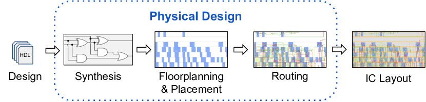
The integrated circuit (IC) design flow starts with design specifications that are converted to register transfer level (RTL) using a hardware description language (HDL). As depicted in Fig. 1, the physical design process synthesizes the design HDL to generate a logic-level netlist comprising macros and standard cells from the technology library. A floorplanning step determines regions and locations for the design’s macros and the IO (input-output) ports. Typically, the standard cells are placed during the placement stage, followed by routing all the design connectivity. The routed design is verified to ensure manufacturability and the physical layout is generated in GDSII format to send to the fabrication unit for manufacturing.
With fixed macro locations, placement is an essential step in the physical design flow to determine the locations of all the standard cells in the design [29, 30, 31, 32]. It significantly impacts the quality and efficiency of the subsequent stages, including routing and manufacturing. The VLSI placement typically consists of three stages: Global Placement, Legalization, and Detailed Placement.
II-A1 Global Placement
In the global placement stage, the placer aims to achieve roughly legal cell locations by distributing the cells across the chip area to minimize overlaps. In addition, the placer also targets other objectives, such as minimizing wirelength and ensuring timing constraints are met.
Wirelength-driven Placement: A wirelength-driven placer aims to minimize the overall wirelength while ensuring minimal cell overlap, as specified in Eqn. 1 [33].
| (1) |
where is the location of cells in the placement, and denotes the total wirelength of all cells in the design. is a density measure of the overlaps among the cells, and it should be below the threshold .
Timing-driven Placement: A timing-driven placer prioritizes optimizing timing critical paths in the design while ensuring the overlaps among the cells are minimum [34]. Given a timing endpoint (a primary output port or an input pin of memory element) with an arrival time of and a required arrival time , the slack of is calculated as follows,
| (2) | ||||
With the timing endpoints in the design, the total negative slack TNS and the worst negative slack WNS are computed as shown in Eqn. 2. A timing-driven placer optimizes either the WNS or the TNS to meet the timing constraint of the design.
II-A2 Legalization
II-A3 Detailed Placement
The detailed placement stage refines the legalized placement to improve design metrics such as wirelength or timing constraints [38, 39]. The refinement can be achieved by operations like (i) Swapping the positions of two cells to improve the objectives without causing legality or timing violations and (ii) Window-based approaches to find optimal cell locations within the specified region.
II-B Watermarking in IC Design
Watermarking [13, 14, 15] encodes unique and confidential signatures into the IC layouts to assist product owners in proof of ownership. Design houses leverage this technique to enhance IP rights protection in the chip supply chain and detect unauthorized usages or replications. These watermarks are typically inserted in the logic design or physical design level.
II-B1 Logic Design Watermarking
The watermarking at the logic design level focuses on safeguarding the Register Transfer Level (RTL) or netlist ownership. Designers embed unique signatures into the RTL or netlist that do not impact the core functionality and are invisible upon adversaries’ inspection. The signature insertion can be categorized as follows: (i) modifying the finite state machine (FSM) to add additional inputs or unused components as watermarks [3, 4]; (ii) adding additional power components as side-channel signatures [40, 41]; and (iii) introducing unique triggers during netlist design that induces the malfunctions when the triggers are detected [42].
More recent works introduce logic locking to add additional logic gates and circuits that alter the original design’s functionality when the incorrect key is applied [43, 44]; obfuscation to adding dummy logic gates or additional circuit connections to make the logic design appear differently from the original one [45, 46]. These techniques are orthogonal to the logic design watermarking, which can be combined to establish more robust intellectual property protection (IPP) frameworks.
II-B2 Physical Design Watermarking
The watermarking at the physical design level encodes signatures onto the IC layout from two directions: (i) constraint-based watermarking [16, 17, 18, 19, 20] that uses cell position/topology as the additional constraints during physical design; (ii) invasive watermarking [5, 21, 6] that adds redundant cells or wires as the watermark signatures.
It is beneficial to watermark at the physical design stage instead of the logic design for these reasons. (i) Adding additional watermarks into the logic design needs to consider physical design criteria like timing to maintain chip quality. However, watermarking after these constraints have been optimized at the physical design stage reduces such discrepancies. (ii) In logic design, if the logic circuits are not performing correctly after watermark insertion, designers need to revisit the RTL design in the previous stage. Physical watermarking, however, does not modify the circuits’ functionalities and only changes how cells are placed or connected on the canvas.
II-B3 Comparison
The watermarking frameworks’ quality is evaluated by the following metrics.
Criteria 1 - Fidelity: The watermarked layouts shall incur minimal quality degradation compared with non-watermarked ones on metrics like wirelength and timing. Besides, the watermarked layouts should adhere to the layouts’ design constraints, such as fence regions and row alignments.
Criteria 2 - Efficiency: The watermarking framework shall be efficient with minimal overheads for watermark insertion.
Criteria 3 - Robustness: The watermarked layout shall be robust against various attacks targeting to remove or forge the signature.
Note that there are other metrics like stealthiness, where watermarked layouts are invisible upon inspection, and effectiveness, in which the watermark shall be successfully extracted. The watermarking frameworks above all possess such properties. Therefore, we skip the evaluations in Table I.
| Stage | WM Method | Fidelity | Efficiency | Robustness | ||||
|---|---|---|---|---|---|---|---|---|
|
|
|||||||
| Physical Design |
|
|||||||
|
||||||||
| ICMarks |
As listed in Table I, during the logic design watermarking [3, 40, 42], the impact of layout quality and robustness depends on the design of the signature insertion algorithms. The watermark encoding also has to consider the physical design criteria in the later stages, and if certain requirements or design specifications are not met, the designers need to revisit the logic design for updates. Such alignments make it less efficient to insert watermarks at the logic design stage.
The constraint-based watermarking frameworks [19, 20, 16, 17, 18] encodes signatures during the placement stage of physical design. The watermarking frameworks did not consider the new design constraints, such as macros and fence regions could lead to performance degradation. In addition, the overhead of watermark insertion remains negligible compared to the time required to optimize the IC layout. The watermarks are embedded as part of the layout. By encoding the constraints into the layout, constraint-based watermarking are robust against removal or forging attacks.
By adding redundant cells/wires, the invasive watermark [5, 21, 6] is efficient for watermark insertion, and the quality degradation depends on how the corresponding algorithm designs the insertion mechanism. Nevertheless, the encoded watermarks can be forged if the adversaries have knowledge of the watermarking algorithm.
In this work, we propose a layout watermarking scheme ICMarks that combines region and position constraints. It can be seamlessly integrated into the physical design pipeline without degrading the layout performance or violating IC design constraints. Besides, its two-level strategic watermark insertion augments its watermarking strength and makes it exceedingly hard for the adversary to remove or counterfeit the signature.
III Problem Formulation
In this section, we introduce ICMarks’s goal and its threat model.
III-A Watermarking Goal
In the physical design stage, the IC design company invests huge efforts in identifying and fine-tuning optimization objectives for better cell placement and net routing. The optimization and customization are infused into different levels of the final layout, including (but not limited to) blocks and cells, to boost IC performance and reduce manufacturing expenses. As such, the final IC layouts constitute invaluable intellectual property, emphasizing the need to safeguard it.
ICMarks establishes ownership proof for the VLSI physical design by inserting watermarks into the placement stage, thereby authenticating the IP for the final layout. Fig. 2 depicts a typical scenario within the supply chain. The IC design company uses highly customized and optimized placement and routing algorithms to enhance physical design quality. The layout from the physical design stage is watermarked and sent to the fabrication company for manufacturing. The manufactured ICs are verified for their functionalities in the test company. The design company can employ reverse engineering approaches [24, 25] to extract the logic netlist and all standard cell locations from an IC layout in GDSII format, and employ ICMarks to decode the signature for ownership verification.

III-B Threat Model
The adversary in the fabricate or test company aims to steal the layout and stop from claiming its ownership by executing different attacks.
Adversary’s Locations: We consider the adversary to be in the fabrication or test company and has access to the layouts produced by the design company.
Adversary’s Objective: Adversary ’s objective is to (i) prevent design company from ownership proof by removing or forging the encoded signature; (ii) the attacked layout performance, such as wirelength or timing metrics shall not be significantly compromised.
Adversary’s Capacities: We consider an adversary with the following capacities: (i) The adversary has access to the layout . However, he cannot reverse-engineer the optimizations and customizations to reproduce because they are infused into every level of the design. (ii) The adversary has access to open-source physical design tools to remove or forge the watermark. He also knows the general algorithms to watermark the layout. However, the random seeds, signatures, and insertion parameters are beyond his reach.
IV ICMarks Design
This section presents the proposed layout watermarking ICMarks, a two-level scheme that inserts watermarks during multiple stages of VLSI placement. In Section IV-A, we introduce the Global Watermarking method. Next, we propose an independent embedding of the watermark signatures as Detailed Watermarking in Section IV-B. While Global and Detailed Watermarking can be used independently for IP protection, ICMarks combines both techniques to take advantage of their best properties.
IV-A Global Watermarking (GW)
Global Watermarking embeds watermarks during the global placement stage. The watermarks, including a pre-defined watermarked region and associated cells in the region, are embedded as a co-optimization term during global placement. The co-optimization objective is to ensure only those associated cells are placed in the watermarked region.
IV-A1 GW Watermark Selection
Given the original, optimized placement denoting the position of all cells as , we employ a sliding window-based algorithm that traverses the placement to search for a region to watermark as in Fig. 3. An ideal watermarked region should meet three criteria: (i) the number of cells within the region should be sufficient to accommodate the required number of signature bits ; (ii) the total cell area within the watermark region are shall be small, thereby providing ample space for watermarked cells to maneuver; and (iii) the cells area overlap on the watermarked region boundary shall be minimized, such that their displacement from the watermarked region has minimal impact on the layout performance. These requirements are incorporated into an evaluation function , as illustrated in Eqn. 3, to evaluate each region of the original placement .
| (3) |
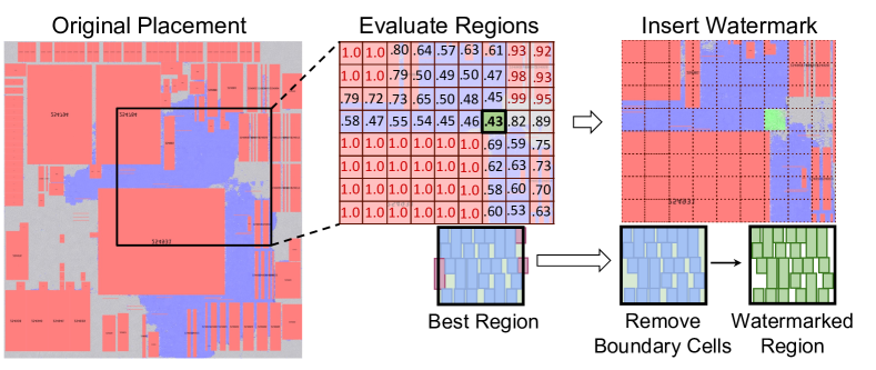
The scoring function is balanced by adjusting the weights , , , where . The scores of the traversed regions are then normalized into a range of . For regions that are nested within macros or other fence regions and any region where , the evaluation function yields the highest evaluation scores as 1.0, rendering the regions not suitable for inserting GW watermarks. The region with the minimum score is chosen as our target watermarked region , and the set of associated cells within the region is denoted as .
IV-A2 GW Watermark Insertion
The watermarked region and its associated cells is formulated as the additional watermarked region constraint in the placement objective. It enforces the associated cells to be in the watermarked region and other cells to be out of . For a design with fence regions, the placement formulation includes watermarked region as the additional optimization constraints, as specified in Eqn. 4 [47].
| (4) |
is the wirelength term and is the cell density term with density multiplier . denotes the location of cell and is the design net. The watermarked region is added as an additional region constraint with associated cells to obtain a watermarked placement .
GW Watermark Strength: Different hyperparameter settings , , result in different minimum-scored watermarked regions and associated cells. The p-value denoted as in statistical Null Hypothesis test [48] measures the probability of a layout carrying the watermark purely by coincidence. A smaller means a stronger watermark signature insertion. The probability that an overlapping cell is out of the watermarked region is denoted as , and the probability that the overlapping cell is in or overlaps is . We measure the probability that or more cells match the watermarking condition, that is, they are out of the watermarked region, as the probability of in Eqn. 5. Here, is the number of combinations of selecting elements from distinct elements. The placement algorithms tend to place cells more compactly, which means the probability of a cell being away from its original place . In Eqn. 5, is an increasing function of when . For simplicity of computation, we set as an upper bound for . In reality, is even smaller because the position and size of the watermarked region are not revealed to the adversary, and it introduces more randomness to strengthen .
| (5) |
IV-A3 GW Watermark Extraction
The design owner asserts ownership by employing the watermarked region to extract cells within the region and comparing these with the associated cells and non-associated cells . The extraction rate of the watermark, denoted as , is calculated in Eqn. 6.
| (6) |
IV-B Detailed Watermarking (DW)
In Detailed Watermarking, the watermarked cells are embedded by moving them slightly along the x- or y-axis after legalization. A follow-up detailed placement stage compensates for the performance degradation from the watermark insertion.
IV-B1 DW Watermark Selection
The Detailed Watermarking moves cells along the x- or y-axis to insert watermarks into the design. Randomly selecting watermarked cells and moving them without considering the dense interconnection could lead to significant performance degradation. To avoid this, Detailed Watermarking only selects cells that will not overlap with their neighbors after cell movements as the watermark as shown in Fig. 4.
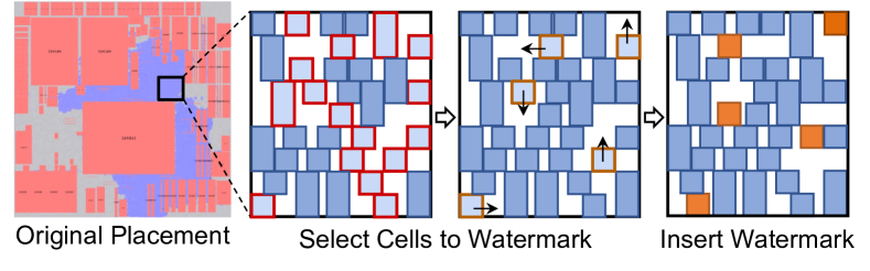
Algorithm 1 outlines how Detailed Watermarking identifies cells that will not overlap with neighbors during watermarking movements and subsequently inserts the signature. It starts by comparing the positions of cells within each row and identifying the cell indices that can move along the x-axis. Then, the algorithm compares cells across adjacent rows to determine if they can be moved up or down for . The cells with room along the x-axis and with room along the y-axis are identified as candidate cells for watermarking. and are associated with these candidate cells to retain a record of their movement directions and distances.
IV-B2 DW Watermark Insertion
At the end of legalization with placement , cells are moved along the x- or y-axis to insert unique watermark signatures hashed as bit sequences . If the -th bit in the signature is 1, the cell randomly selected from the candidate watermarked cell set is moved along the x-axis for . If the -th signature bit is 0, the cell is randomly chosen from the candidate watermarked cell set and moved along the y-axis for . The resulting placement is denoted as intermediate placement , and the indices of the cells moved along the x- or y-axis form the watermarked cells . These movements are performed before detailed placement, allowing possible performance degradation to be compensated during the subsequent detailed placement phase and yield a watermarked solution . The selected watermarked cells , and their corresponding position distance between intermediate placement and the watermarked placement constitute the watermark.
DW Watermark Strength: The p-value to measure the probability of a layout carrying the watermark purely by coincidence can be formulated by Eqn. 7. is the probability of cells moving along the x-axis being the same as the watermarked cells, and is the probability of cells moving along the y-axis being the same as the watermarked cells.
| (7) |
In Eqn. 8, is the probability of or more cells match the watermarked cells along x-axis as , and the is the probability of the watermarked cells are chosen from all of the candidate cells . Similarly, is the probability of or more cells match the watermarked cells along the y-axis, and the . Given and , the above and can be viewed as the approximate probability for no replacement watermarked cell selection.
| (8) |
IV-B3 DW Watermark Extraction
The design owner detects watermarks in the placement by comparing the watermarked cell position with the intermediate placement and calculates the new distance as . If cells in the extracted matches the both along x- and y-axis, the watermark extraction rate is calculated as Eqn. 9.
| (9) |
IV-C ICMarks Watermarking
As a combination of both the GW and the DW, ICMarks applies global watermarking during its global placement stage and detailed watermarking on top of the watermarked region before its detailed placement stage. By combining these two watermarking schemes, the inserted watermark strength is further augmented.
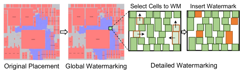
IV-C1 ICMarks Watermark Insertion
As in Fig. 5, ICMarks employs a hybrid approach that combines Global and Detailed Watermarking to produce stronger watermarks. Initially, ICMarks searches for a watermarked region using the strategy akin to Global Watermarking, yielding a watermarked region and associated cells . ICMarks runs global placement and legalization with such watermark constraints. Then, it perturbs cells along the x- and y-axis within the watermarked region , following the approach of Detailed Watermarking and obtain an intermediate placement . Afterward, the detailed placement proceeds to compensate for watermarking degradation and produce the watermarked placement . The perturbed distance and cells are the watermarks in the second step.
ICMarks Watermark Strength: Due to the combination of global and detailed watermarking, the watermark strength of ICMarks is further augmented. To coincidentally carry the watermark, one has to overcome both the signatures from the global and detailed watermarking. Given the watermark strength of the global watermarking to be and the detailed watermarking to be , where the and are changed to the number of cells available to move in the watermarked region. We get the ICMarks’s as in Eqn. 10, further minimizing the coincidental probability.
| (10) |
IV-C2 ICMarks Watermark Extraction
To claim ownership of the layout, given the cell positions , the watermark holder can use the following two steps. (i) The extraction of the watermarks from the watermarked region , with the global extraction rate denoted as in Eqn. 6. (ii) Afterwards, the inserted signatures are extracted by comparing with at the watermarked cell indices . The number of cells successfully matched is denoted as , from which the detailed extraction rate is calculated as in Eqn. 9. The final WER is calculated in Eqn. 11.
| (11) |
V Experiments
In this section, we first introduce the experiment setups in Section V-A. Then, we evaluate the performance of wirelength-driven and timing-driven design watermarking in Section V-B. Next, we show the robustness of ICMarks under attacks in Section VI.
V-A Experimental Setup
Datasets: We evaluate the watermarking impact on wirelength-driven benchmark suites: ISPD’2015 [26] and ISPD’2019 [27]; and the timing-driven ICCAD’2015 [28] benchmark suite. All designs in the ICCAD’2015 benchmark suite are large and contain more than 700k cells. The statistics of these designs are summarized in Table II, with designs having fence regions marked in blue. The macros, fence regions, and IO pin locations in the benchmarks are fixed.
| Suite | Design | Cells | Nets | Size | Stride | |||
|---|---|---|---|---|---|---|---|---|
| perf_a | 108K | 115K | 10 | 5 | 0.1 | 0.1 | 1 | |
| perf_b | 113K | 113K | 10 | 5 | 0.1 | 0.1 | 1 | |
| dist_a | 127K | 134K | 20 | 5 | 0.1 | 0.1 | 1 | |
| mult_b | 146K | 152K | 10 | 5 | 0.1 | 0.1 | 1 | |
| mult_c | 146K | 152K | 20 | 5 | 0.1 | 0.1 | 1 | |
| pci_a | 30K | 34K | 10 | 5 | 0.1 | 0.1 | 1 | |
| pci_b | 29K | 33K | 20 | 5 | 0.1 | 0.1 | 1 | |
| superblue11 | 926K | 936K | 100 | 40 | 0.1 | 0.5 | 1 | |
| superblue16 | 680K | 697K | 50 | 10 | 0.1 | 0.1 | 1 | |
| perf_1 | 113K | 113K | 50 | 10 | 0.1 | 0.5 | 1 | |
| fft_1 | 35K | 33K | 10 | 5 | 0.1 | 0.1 | 1 | |
| fft_2 | 35K | 33K | 10 | 5 | 0.1 | 0.1 | 1 | |
| fft_a | 34K | 32K | 10 | 5 | 0.1 | 0.1 | 1 | |
| fft_b | 34K | 32K | 20 | 5 | 0.1 | 0.1 | 1 | |
| mult_1 | 160K | 159K | 50 | 10 | 0.1 | 0.5 | 1 | |
| mult_2 | 160K | 159K | 50 | 10 | 0.1 | 0.5 | 1 | |
| mult_a | 154K | 154K | 50 | 10 | 0.1 | 0.5 | 1 | |
| superblue12 | 1293K | 1293K | 50 | 10 | 0.1 | 0.1 | 1 | |
| superblue14 | 634K | 620K | 50 | 10 | 0.1 | 0.1 | 1 | |
| ISPD 2015 (WL) | superblue19 | 522K | 512K | 100 | 10 | 0.1 | 0.5 | 1 |
| ispd19test1 | 9K | 3K | 10 | 5 | 0.1 | 0.1 | 1 | |
| ispd19test2 | 73K | 72K | 10 | 5 | 0.1 | 0.1 | 1 | |
| ispd19test3 | 8K | 9K | 20 | 5 | 0.5 | 0.1 | 1 | |
| ispd19test4 | 151K | 146K | 10 | 5 | 0.1 | 0.1 | 1 | |
| ispd19test5 | 29K | 29K | 10 | 5 | 0.1 | 0.1 | 1 | |
| ispd19test6 | 181K | 180K | 50 | 10 | 0.1 | 0.1 | 1 | |
| ispd19test7 | 362K | 359K | 100 | 10 | 0.1 | 0 | 1 | |
| ispd19test8 | 543K | 538K | 50 | 10 | 0.1 | 0.5 | 1 | |
| ispd19test9 | 903K | 895K | 200 | 20 | 0.1 | 0.1 | 1 | |
| ISPD 2019 (WL) | ispd19test10 | 903K | 895K | 200 | 20 | 0.1 | 0.5 | 1 |
| superblue1 | 1209k | 1215k | 100 | 50 | 0.1 | 0 | 1 | |
| superblue3 | 1213k | 1224k | 100 | 30 | 0.1 | 0 | 1 | |
| superblue4 | 795k | 802k | 100 | 50 | 0.1 | 0 | 1 | |
| superblue5 | 1086k | 1100k | 100 | 50 | 0.1 | 0.1 | 1 | |
| superblue7 | 1931k | 1933k | 100 | 30 | 0.1 | 0 | 1 | |
| superblue10 | 1876k | 1898k | 100 | 30 | 0.1 | 0.1 | 1 | |
| superblue16 | 981k | 999k | 100 | 30 | 0.1 | 0 | 1 | |
| ICCAD 2015 (Timing) | superblue18 | 768k | 771k | 100 | 50 | 0.1 | 0 | 1 |
Experiment Setup: ICMarks is implemented with Python 3.9 and benchmarked on a Linux Ubuntu system equipped with NVIDIA TITAN XP GPUs, each with 12 GB RAM, and 48 Intel(R) Xeon(R) CPUs, accompanied by 128 GB RAM. The watermarking methodology of ICMarks can be integrated into any VLSI physical design framework, and we chose to build upon the open-source placement framework, DREAMPlace [47] to demonstrate its viability. The DREAMPlace [47] accelerates the state-of-the-art placement algorithm ePlace [49]/RePlAce [50] on a GPU and maintains the same level of performance. For routing, we employ the open-source state-of-the-art framework CUGR [51]. For timing-driven benchmark suite, we use DREAMPlace 4.0 [34] where the timing metrics are measured by OpenTimer [52].
Hyperparameters: For the hyperparameters, we perform a grid search for the GW phase. In the search of Eqn. 3, the = {0.1, 0, 0.5}, ={0.1, 0, 0.5}, and = 1. The search terminates when the watermarked layout quality is not compromised. For all the considered benchmark suites, we report the GW hyperparameters in Table II. In the DW phase, , and is set to one adjacent row-height.
Baseline: We choose the following state-of-the-art watermarking frameworks as our baselines: (i) topology constraint-based Row Parity [20, 19] that inserts unique bit sequences as watermarks by shifting cells to different rows in the placement stage. Cells with a 1-bit are moved to an odd row, while cells with a 0-bit are moved to an even row; (ii) position constraint-based Cell Scattering [5] that employs pseudorandom coordinate transformation (PRCT) algorithms to scatter the watermarked cells on the chip canvas as watermarks. Cells with 1-bit are moved along the y-axis, and cells with 0-bit are moved along the x-axis if they do not overlap with their neighbors; (iii) invasive Buffer Insertion [6] that adds additional buffers as watermarks without affecting timing critical paths during the placement stage. Two buffers are inserted to represent 0-bit, and one buffer is inserted to represent 1-bit.
We skip the baselines that: (i) have different watermarking targets. [18, 17] are designed for smaller full-custom IC designs, [53, 54] are designed for FPGAs, whereas our watermarking targets are modern digital VLSI designs; (ii) have similar watermarking approaches as our baselines, and we use the baselines as a proof-of-concept. [16] inserts flip-flops instead of buffers into the layouts as watermarks. The signature length is set to 50-bit for all frameworks.
| Row Parity [20, 19] | Cell Scattering [5] | Buffer Insertion [6] | ICMarks: GW | ICMarks: DW | ICMarks: GW+DW | |||||||
| Design | PWLR | RWLR | PWLR | RWLR | PWLR | RWLR | PWLR | RWLR | PWLR | RWLR | PWLR | RWLR |
| perf_a | 1.0045 | 1.0155 | 0.9978 | 0.9967 | 1.5289 | 2.3270 | 0.9976 | 0.9873 | 0.9994 | 1.0003 | 0.9972 | 0.9873 |
| perf_b | 1.0058 | 1.0267 | 1.0020 | 1.0001 | 1.0176 | 1.0745 | 0.9930 | 0.9901 | 0.9990 | 1.0002 | 0.9890 | 0.9901 |
| dist_a | 1.0015 | 0.9999 | 0.9984 | 0.9965 | 1.0995 | 1.1072 | 1.0004 | 1.0052 | 0.9998 | 1.0005 | 1.0004 | 1.0052 |
| mult_b | 1.0047 | 1.0199 | 0.9991 | 0.9923 | 1.8966 | 2.9374 | 1.0010 | 1.0028 | 1.0002 | 1.0044 | 0.9994 | 1.0028 |
| mult_c | 1.0031 | 1.0252 | 0.9980 | 1.0023 | 1.6003 | 2.7459 | 1.0017 | 0.9979 | 0.9990 | 1.0020 | 0.9963 | 0.9979 |
| pci_a | 1.0080 | 1.0340 | 0.9931 | 0.9846 | 1.6269 | 1.6849 | 1.0361 | 1.0048 | 1.0011 | 1.0021 | 0.9997 | 0.9950 |
| pci_b | 1.0069 | 1.1173 | 0.9912 | 0.9977 | 1.2239 | 1.8207 | 0.9951 | 1.0026 | 0.9997 | 1.0008 | 0.9951 | 1.0026 |
| superblue11 | 1.0052 | 1.0344 | 1.0278 | 1.0358 | 1.6930 | 3.7086 | 0.9992 | 0.9992 | 0.9995 | 1.0005 | 0.9986 | 0.9992 |
| superblue16 | 1.0030 | 1.0210 | 0.9988 | 0.9989 | 1.1023 | 1.1377 | 1.0018 | 1.0204 | 1.0000 | 1.0000 | 1.0017 | 1.0204 |
| perf_1 | 1.0035 | 1.0199 | 0.9985 | 0.9983 | 1.0150 | 1.0642 | 1.0031 | 0.9973 | 1.0042 | 1.0019 | 0.9964 | 0.9973 |
| fft_1 | 1.0017 | 1.0260 | 1.0167 | 1.0156 | 1.0680 | 1.1457 | 0.9671 | 0.9673 | 1.0026 | 0.9975 | 0.9671 | 0.9673 |
| fft_2 | 1.0050 | 1.0260 | 1.0148 | 1.0114 | 1.4603 | 1.4476 | 0.9767 | 0.9770 | 1.0027 | 0.9996 | 0.9767 | 0.9770 |
| fft_a | 1.0121 | 1.0200 | 1.0024 | 0.9933 | 1.8203 | 2.1923 | 0.9939 | 0.9895 | 1.0075 | 1.0094 | 0.9939 | 0.9895 |
| fft_b | 1.0018 | 1.0075 | 0.9961 | 1.0030 | 1.9859 | 2.5615 | 0.9909 | 0.9890 | 0.9991 | 1.0036 | 0.9909 | 0.9890 |
| mult_1 | 1.0050 | 1.0238 | 1.0077 | 1.0065 | 1.0464 | 1.0631 | 0.9753 | 0.9744 | 1.0004 | 1.0008 | 0.9753 | 0.9744 |
| mult_2 | 1.0033 | 1.0199 | 0.9984 | 0.9967 | 1.0736 | 1.1147 | 0.9867 | 0.9900 | 0.9990 | 0.9992 | 0.9852 | 0.9900 |
| mult_a | 1.0037 | 1.0105 | 0.9995 | 0.9968 | 1.3862 | 1.6738 | 0.9973 | 0.9916 | 1.0005 | 0.9958 | 0.9973 | 0.9916 |
| superblue12 | 1.0031 | 1.0067 | 0.9979 | 0.9956 | 1.0683 | 1.1044 | 1.0036 | 0.9732 | 0.9994 | 0.9942 | 0.9854 | 0.9732 |
| superblue14 | 1.0020 | 1.0057 | 0.9991 | 0.9981 | 1.0212 | 1.0286 | 0.9851 | 0.9867 | 1.0001 | 1.0000 | 0.9887 | 0.9867 |
| superblue19 | 1.0025 | 1.0077 | 1.0001 | 1.0005 | 1.0295 | 1.0672 | 0.9881 | 0.9809 | 1.0003 | 1.0001 | 0.9814 | 0.9809 |
| Average: FR | 1.0047 | 1.0322 | 1.0006 | 1.0005 | 1.0724 | 1.1061 | 1.0028 | 1.0011 | 0.9997 | 1.0012 | 0.9975 | 1.0000 |
| Average: All | 1.0043 | 1.0231 | 1.0018 | 1.0012 | 1.0536 | 1.0901 | 0.9946 | 0.9913 | 1.0007 | 1.0006 | 0.9908 | 0.9908 |
| Row Parity [20, 19] | Cell Scattering [5] | Buffer Insertion [6] | ICMarks: GW | ICMarks: DW | ICMarks: GW+DW | |||||||
| Design | PWLR | RWLR | PWLR | RWLR | PWLR | RWLR | PWLR | RWLR | PWLR | RWLR | PWLR | RWLR |
| ispd19test1 | 1.0060 | 1.0129 | 0.9978 | 0.9998 | 1.0394 | 1.0619 | 0.9995 | 1.0015 | 1.0023 | 1.0043 | 0.9955 | 1.0015 |
| ispd19test2 | 1.0184 | 1.0201 | 1.0096 | 1.0016 | 1.0127 | 1.0408 | 0.9981 | 0.9999 | 1.0021 | 1.0003 | 0.9988 | 0.9999 |
| ispd19test3 | 1.0130 | 1.0475 | 1.0180 | 1.0193 | 1.0582 | 1.0801 | 1.0059 | 1.0045 | 0.9961 | 0.9976 | 1.0059 | 1.0045 |
| ispd19test4 | 1.0017 | 1.0050 | 0.9999 | 0.9998 | 1.1452 | 1.2494 | 0.9957 | 0.9907 | 0.9998 | 1.0028 | 0.9957 | 0.9907 |
| ispd19test5 | 1.0102 | 1.0556 | 1.0998 | 1.0975 | 0.9859 | 1.0121 | 1.0013 | 0.9998 | 0.9996 | 0.9968 | 1.0013 | 0.9998 |
| ispd19test6 | 1.0032 | 1.0106 | 0.9994 | 0.9993 | 1.0044 | 1.1108 | 1.0023 | 1.0026 | 1.0001 | 0.9997 | 1.0023 | 1.0026 |
| ispd19test7 | 1.0028 | 1.0160 | 1.0136 | 1.0109 | 1.0003 | 1.0717 | 1.0050 | 1.0054 | 1.0000 | 0.9997 | 1.0050 | 1.0054 |
| ispd19test8 | 1.0001 | 1.0082 | 0.9966 | 0.9958 | 1.0118 | 1.0806 | 0.9961 | 0.9929 | 0.9999 | 0.9996 | 0.9961 | 0.9929 |
| ispd19test9 | 1.0072 | 1.0108 | 1.0108 | 1.0095 | 1.0164 | 1.0814 | 1.0023 | 1.0023 | 1.0009 | 0.9999 | 1.0023 | 1.0023 |
| ispd19test10 | 1.0025 | 1.0090 | 1.0043 | 1.0108 | 1.0378 | 1.0982 | 0.9972 | 0.9967 | 0.9999 | 1.0002 | 0.9972 | 0.9966 |
| Average | 1.0065 | 1.0194 | 1.0060 | 1.0140 | 1.0304 | 1.0871 | 1.0003 | 0.9996 | 1.0001 | 1.0001 | 1.0000 | 0.9996 |
Evaluation Metrics: For the wirelength-driven benchmark suites, whose quality is measured by the layout wirelength, we use three metrics to evaluate the watermark performance:(i) Placement WireLength Rate (PWLR): The rate of estimated half-perimeter wirelength (HPWL) of watermarked layout compared to the original one; (ii) Routing WireLength Rate (RWLR): The rate of routed wirelength of watermarked layout compared to the original one; (iii) Watermark Extraction Rate (WER): The percentage of signatures extracted from the watermarked layout. For the timing-driven benchmark suite, whose quality is measured by the timing slack, we use three metrics to evaluate the performance under static timing analysis [52]: (i) Total Negative Slack Rate (TNSR): The rate of total negative slack (TNS) of watermarked layout compared to original one; (ii) Worst Negative Slack Rate (WNSR):The rate of worst negative slack (WNS) of watermarked layout compared to original one; (iii) Watermark Extraction Rate (WER): The percentage of signatures extracted from the layout. The rate average is calculated by the geometric mean [55] of designs’ metrics.
| Row Parity [20, 19] | Cell Scattering [5] | Buffer Insertion [6] | ICMarks: GW | ICMarks: DW | ICMarks: GW+DW | |||||||
| Design | TNSR | WNSR | TNSR | WNSR | TNSR | WNSR | TNSR | WNSR | TNSR | WNSR | TNSR | WNSR |
| superblue1 | 1.0053 | 1.0094 | 1.0119 | 1.0026 | 1.0083 | 1.0020 | 0.9001 | 0.8514 | 1.0256 | 1.0249 | 0.8283 | 1.0021 |
| superblue3 | 1.0053 | 1.0176 | 1.0066 | 0.9891 | 1.1035 | 1.0988 | 0.9302 | 0.9029 | 1.0035 | 0.9884 | 0.9363 | 0.9047 |
| superblue4 | 1.1299 | 0.9914 | 0.9698 | 1.0191 | 1.1954 | 1.1995 | 0.9037 | 0.9370 | 0.9554 | 0.9930 | 0.9221 | 1.0094 |
| superblue5 | 0.9801 | 0.9887 | 1.0126 | 0.9977 | 1.0932 | 1.1174 | 0.9159 | 1.0001 | 0.9922 | 0.9959 | 0.9159 | 1.0508 |
| superblue7 | 0.9801 | 0.9932 | 0.9979 | 1.0212 | 0.9933 | 1.0199 | 0.9584 | 0.9758 | 0.9934 | 1.0199 | 0.9636 | 0.9727 |
| superblue10 | 1.0099 | 1.0041 | 1.0218 | 1.0141 | 1.0194 | 1.2918 | 1.0069 | 1.0072 | 1.0058 | 1.0068 | 1.0069 | 1.0072 |
| superblue16 | 0.9814 | 1.1271 | 0.9067 | 1.3274 | 1.0109 | 1.0877 | 1.0166 | 1.0473 | 0.9060 | 1.3485 | 1.0069 | 1.0072 |
| superblue18 | 1.0068 | 0.9965 | 0.9981 | 1.0064 | 1.0438 | 1.0613 | 0.9337 | 0.9403 | 1.0014 | 1.0002 | 0.9254 | 0.9449 |
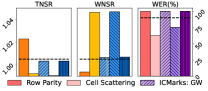
| Average | 1.0114 | 1.0151 | 0.9900 | 1.0424 | 1.0566 | 1.1063 | 0.9448 | 0.9559 | 0.9848 | 1.0418 | 0.9366 | 0.9867 |
To preserve the optimized outcomes from the physical design algorithms, we set a threshold of layout quality degradation to not exceed 0.5%. Because surpassing this threshold would counteract the benefits derived from the performance enhancement efforts in physical design [29].
V-B Experimental Results
V-B1 Wirelength-driven Watermarking Fidelity
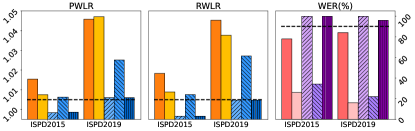
The performance of different watermarking schemes is tabulated in Table III for the ISPD’2015 benchmarks [26], and in Table IV for the ISPD’2019 benchmarks [27]. For all the layouts in Table III-Table IV, their inserted watermarks can be successfully extracted. Therefore, we evaluate how much layout performance is compromised to accommodate such watermark insertion among these watermarking frameworks.
Comparison with Prior Constraint-based Watermarking [20, 19, 5]: Among the two benchmark suites, ICMarks results in no PWLR and RWLR degradation for accommodating the 50-bit signature. In contrast, the topology constraint-based Row Parity [20, 19] changes the row index of the cells to encode watermarks but does not consider potential design constraints (e.g., fence regions and macros) in VLSI design. As a result, it results in 2.31% and 1.94% routed wirelength (RWLR) degradation on ISPD’2015 [26] and ISPD’2019 [27], respectively. The position constraint-based Cell Scattering [5] perturbs cell locations in the optimized layout for signature insertion. However, randomly selecting and moving watermarked cells after the optimization is done results in quality degradation, as reflected by the 0.12% and 1.4% RWLR degradation over the original design on ISPD’2015 [26] and ISPD’2019 [27].
Comparison with Invasive Watermarking [6]: The invasive watermarking Buffer Insertion [6] overlooks the additional design constraints, like fence regions and macros, in the modern VLSI design. The additional 50 buffers might be added close to such design constraints and result in significant cell displacement, as the design has to accommodate the buffers while satisfying the design constraints. As in Table III-Table IV, Buffer Insertion [6] introduced 9.01% and 8.71% routed wirelength (RWLR) degradation on ISPD’2015 [26] and ISPD’2019 [27] benchmarks. ICMarks, however, has no wirelength degradation on both benchmarks. Besides, for the highly-utilized designs, where most of the layout space is filled with standard cell and fixed marcos/fence regions/IO pins, to accommodate the additional buffers, cells have to be displaced significantly from their non-watermarked position for buffer insertion. As such, it introduced significant PWLR and RWLR degradations as the grey numbers in Table III.
DW Insertion Before/After Detailed Placement: After the placement stage is finished, the baseline Cell Scattering [5] moves cells in the layout along the x/y axis if there is space. The key difference is Cell Scattering [5] performs the movement after detailed placement, whereas the ICMarks: DW is performed before detailed placement. As seen in Table III- IV, ICMarks: DW improves the RWLR quality from Cell Scattering [5] by 0.06% and 1.39%, respectively.
Comparison with the GW and DW submodules: As a combination of GW and DW, ICMarks takes advantage of their strength and further reduces the performance degradation from accommodating watermarks. In contrast to GW, ICMarks slightly improves the placement quality. This improvement stems from modifying cell positions within a designated region, either across different rows or along the x-axis. Such modifications inherently disturb solutions formulated during global placement. Given that these disturbances occur in less compact regions, they provide different inputs to the detailed placement process, thereby offering potential optimization trajectories to minimize overall wirelength. The optimization to GW depends on the quality of the perturbations introduced, where the refinement on ISPD’2019 [27] is marginal, and the improvement on ISPD’2015 [26] is 0.05% over GW.
Compared with DW, ICMarks watermarks upon the placement solution from GW, whereas DW watermarks the original solution. The additional co-optimization of the GW watermarked region makes the placer further refine the cell positions in the watermarked region and, thus, improves the watermarked layout quality. By encoding DW signature on the GW layout, ICMarks introduced no quality degradations. In contrast, DW watermarks upon the original placement solution, which could introduce more performance degradation when inserting DW signatures. It is reflected by the 0.06% and 0.01% RWLR improvement over the original design on ISPD’2015 [26] and ISPD’2019 [27] benchmarks, respectively.
V-B2 Timing-driven Watermarking Fidelity
As depicted in Table V, ICMarks continuously preserves the layout quality in timing-driven watermarking benchmark ICCAD’2015 [28]. By strategically searching for the watermarked region and cells with minimal impact on the performance, ICMarks results in no WNS and TNS degradation. On the opposite, the constraint-based Row Parity [20, 19] and Cell Scattering [5] overlook design constraints in modern VLSI design and did not design the watermarking algorithms with the timing optimization objectives. It results in 1.51% and 4.24% WNSR degradation over the original designs, respectively. Furthermore, while Buffer Insertion [6] encodes additional buffers on the non-timing critical path, the inserted buffers still result in 5.66% TNSR and 10.63% WNSR timing metrics degradation.
V-B3 Watermarking Capacity
The watermarking capacity is measured by the maximum length of watermark bits that can be inserted into the layout without significantly degrading the layout quality. For Row Parity [20, 19], Cell Scattering [5], and ICMarks: DW, the signature length corresponds to the moved/inserted cell number. For Buffer Insertion [6], the length is the number of buffer-inserted nets. For ICMarks: GW, the signature length corresponds to the in Eqn. 3. For ICMarks, the signature length corresponds to the cells in global watermarking and moves cell over the watermarked region in the detailed watermarking.
We use ISPD’2019 [27] as the benchmarking target and display the results in Fig. 6. As seen, the maximum bits that can be inserted by Row Parity and Cell Scattering are both less than 30 bits. Both methods move the cells across rows after the detailed placement as watermarks, which leads to worse RWLR than PWLR, as the router has to cross rows to connect the cells. Buffer Insertion [6] inserts signatures without considering the design constraints, leading to significant cell displacement after signature insertion. Therefore, it exhibits low watermarking capacity on ISPD’2019 [27]. The ICMarks: DW’s capacity is larger and reaches 100 bits. Because it moves the cells before detailed placement and the subsequent detailed placement compensates for the watermark insertion. ICMarks: GW and ICMarks further outperform the scheme. They both demonstrate a capacity of more than 200 bits by exploring the less compact region for watermark encoding. Since ICMarks builds the watermarking scheme on top of ICMarks: GW, the two PWLR and RWLR lines are close in Fig. 6.
V-B4 Watermarking Strength
To successfully prove ownership, the owner not only needs to provide the signatures but also the exact distance information for ICMarks: DW; cell ID, and region positions for ICMarks: GW. The watermarking strength, if all watermarks are successfully extracted, is for Row Parity [20, 19], but will be 1.25 for ICMarks following Eqn. 10. As in Table VI, 50-bit signature provides sufficient protection to the layout.
| Signature | ICMarks: GW | ICMarks: DW | ICMarks: GW + DW |
|---|---|---|---|
| 30 bits | 5.68 | 1.91 | 4.93 |
| 50 bits | 1.69 | 7.88 | 1.25 |
| 100 bits | 1.50 | 7.88 | 1.43 |
V-B5 Watermarking Efficiency
The watermarking efficiency is benchmarked by the fraction of the additional time takes for ICMarks’s watermark insertion compared to the overall physical design stage, primarily placement and routing. We include the average time takes to encode 50-bit signatures onto the ISPD’2015 benchmark [26] and ISPD’2019 benchmark [27] in Table VII. The non-WM time and WM time is the average (geometric-mean) time it takes for placement and routing on the non-watermarked and watermarked layout. The Slow Down is the percentage overhead ICMarks introduced to the overall placement and routing phase. As seen, the time taken for watermark insertion is 10% compared with the overall placement and routing stage, making ICMarks efficient for watermarking. Besides, no additional computation resources or external tools are required for the signature insertion.
V-B6 Watermarking Stealthiness
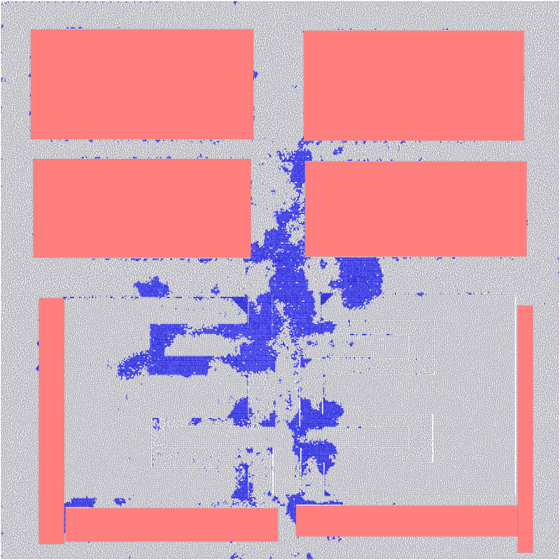
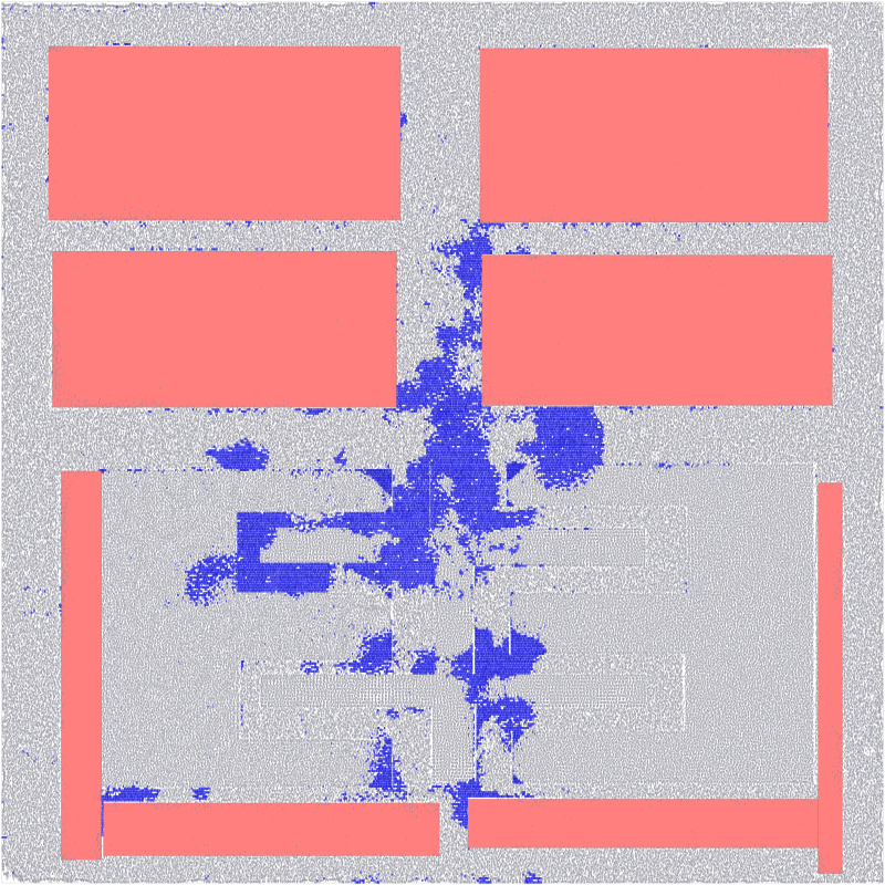
We display the layout watermarked by ICMarks with various sizes and different design constraints in Fig. 7. As seen, the watermarks are embedded as part of the layout, and invisible upon inspection while maintaining 100% WERs.


V-B7 Ownership Proof in Real-World Settings
To prove ownership, the design company obtains the suspicious layout and employs reverse-engineering approaches [24, 25] to acquire the logic netlist and all standard cell locations. Such methodology [24, 25] recovers large layouts netlists (over 7000k cells) from the GDSII layout with over 98% accuracy and efficiency. Then, the design company uses the netlists to recover the standard cells’ and macros’ locations. The watermark extraction algorithms in Section IV are subsequently used for ownership proof. While the reverse-engineering misalignment might degrade the watermark extraction rates slightly, ICMarks still provides sufficient ownership proof for the design companies benefiting from two aspects: (i) high watermarking strength of 1.25 for 50-bit signature and 1.43 for 100-bit signature, as in Table VI; (ii) high watermarking capacity that can accommodate more than 200-bit signatures without significant quality degradation, as in Fig. 6. As a result, even if only 88% signatures are extracted (10% lost from attacks in Section VI and 2% lost from reverse engineering [24, 25]), ICMarks still provides the watermarking strength at the level of and for 50-bit and 100-bit signatures, respectively. In Null Hypothesis [56], a watermarking strength (p-value) of smaller than 0.05 indicates the statistically significant presence of a watermark. Given the much lower watermarking strength than 0.05 after reverse-engineering, the design company can thereby confidently claim ownership of the design layout.
VI Attack Evaluation
In this section, we evaluate ICMarks’s robustness under watermark removal and forging attacks.
VI-1 Watermark Removal Attack
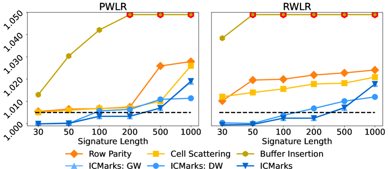
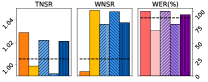
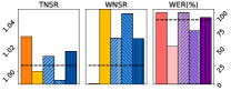
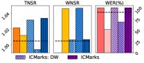
A successful watermark removal attack shall meet two criteria: (i) the encoded signatures are removed as reflected by the watermark extraction rate (WER) below 90% [20, 19]; (ii) the layout quality is not compromised, where the Placement Half-Perimeter WireLength Rate (PWLR), Routed Wirelength Rate (RWLR), Total Negative Slack Rate (TNSR), and Worst Negative Slack Rate (WNSR) do not exceed 1.005 [29]. The thresholds are reflected by the black dotted lines in Fig. 8 and Fig. 9.
For an IC layout watermarked by ICMarks, the watermarks are inserted by constraining the cell positions and cells’ region. To remove the signature, the adversary perturbs the cell positions/regions for watermark removal attacks. We compare four types of attacks aiming to erase the signatures at different levels of watermarking and prevent the owner from claiming ownership: (i) swap location attacks (SLA) [19], which target to attack Row Parity framework by random swapping cell locations, (ii) constraint perturbation attacks (CPA), which target to attack Cell Scattering and ICMarks: DW by moving cells along x/y axis if there is space; (iii) Optimization attacks (OA), which target to attack all watermarking frameworks by running another round of detailed placement; and (iv) adaptive region attacks (ARA), which target to attack ICMarks: GW and ICMarks framework by searching for less compacted regions and perturb cells around the region. We show ICMarks is robust against all removal attacks, and the results are summarized in Fig. 8 and Fig. 9 for wirelength-driven and timing-driven placements respectively.
We skip Buffer Insertion [6] and the corresponding watermark removal attacks because (i) Buffer Insertion’s [6] watermarked layout quality degradation is significantly higher than the considered threshold of 0.5% as in Table III-V; (ii) Other watermarking frameworks insert signatures without modifying the netlist, whereas Buffer Insertion [6] encodes adding buffers into the netlist as watermarks. While the buffer removal attacks, which remove multiple cascaded buffers, can potentially erase Buffer Insertion’s signature, our primary goal is evaluating the robustness of ICMarks under attacks. Therefore, we did not include the attacks at the netlist level in this section.
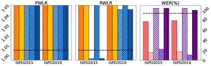
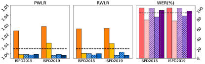
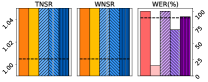
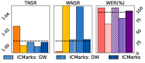
Swap Location Attacks (SLA): In SLA [19], cells randomly exchange their locations with another set of cells. Then, a follow-up legalization and external detailed placement engine NTUPlace4dr [57] compensate for the performance degradation and ensure the cells follow the design rules. In Fig. 8a and Fig. 8b, we randomly choose 0.1% and 0.5% cells from the layout and pair them to exchange their locations. As seen, even small location swaps result in huge performance degradation on modern IC layouts. In terms of the watermark extraction, Row Parity [20, 19], Cell Scattering [5], and ICMarks: DW get WERs below 90% and failed to verify their ownership. Those watermarking frameworks spread the watermarks across the layout, where minor changes will subsequently modify most cell locations within the compact region. By embedding cells in the less compact region, ICMarks: GW and ICMarks are less sensitive to such changes. As a result, ICMarks: GW and ICMarks still maintain high WERs.
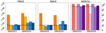
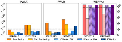
Constraint Perturbation Attacks (CPA): In CPA, cells shift their location along the x-axis for or y-axis for set to one adjacent row-height if such movements do not result in overlapping with their neighbors. In Fig. 8c, Fig. 8d, and Fig. 8e, we move the positions of 0.1%, 1%, 10% of the cells have space to move in the layout. From here, we find that under CPA 0.1% attack, layout performance hit the boundary of the wirelength degradation (PWLR and RWLR) threshold. For the watermark extraction, ICMarks, ICMarks: GW, and Row Parity [20, 19] achieve over 90% WER. However, the WER of Cell Scattering [5] and ICMarks: DW are subsequently lower than 90% because the constraint perturbation targets to remove the potential watermarked cell positions.
For the CPA 1% and 10% cell performance, however, the PWLR and RWLR degradations are greater than 1.005, meaning the attack failed to maintain the layout quality improvement from the design company’s physical design optimizations. But ICMarks: GW and ICMarks still maintain higher than 90% WER and successfully help the design company to claim ownership of the layout.
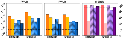
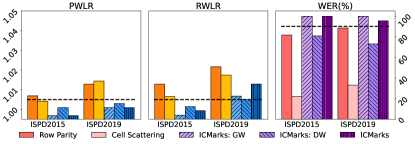
Optimization Attacks (OA): This attack employs an additional optimization stage to remove the watermarks. The optimization is implemented through another round of detailed placement from an external open-source placer NTUPlace4dr [57]. It aims to change cell locations slightly for signature removal while maintaining the layout quality. As shown in Fig. 8f, the layout wirelength degradation in Cell Scattering [5], ICMarks: GW, ICMarks: DW, and ICMarks are all below 1.005, indicating the attack preserves the layout quality. The WER of Cell Scattering [5] and ICMarks: DW are below 90%, meaning OA successfully removed their signatures. In contrast, ICMarks: GW and ICMarks have over 90% WER, demonstrating their resiliency.
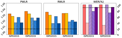
Adaptive Region Attacks (ARA): This attack targets to remove watermarks in ICMarks:GW. The adversary has prior knowledge of how ICMarks:GW performs the watermarking and has access to the hyperparameters used to search the watermarked region. The adversary operates on top of the watermarked layout. He tries to remove the inserted watermarks by moving cells within the searched top-1 or top-5 regions if there is room. In Fig. 8g and Fig. 8h, the PWLR and RWLR degradation for ICMarks: GW, ICMarks: DW, and ICMarks are around the threshold of 0.5% degradation, and the attacks do not significantly degrade the layout quality. The WER of ICMarks: GW and ICMarks remain over 90%. As the watermark insertion is performed on a non-watermarked layout, and the attack regions searched by ARA are on a watermarked layout, the watermark signatures are not the same. Therefore, ARA fails to remove ICMarks: GW and ICMarks’s signature, even if the same region watermarking algorithm is employed. In contrast, the watermarks of Row Parity [20, 19], Cell Scattering [5], and ICMarks:DW are spread across the layout, where minor changes in the compact area will subsequently modify the inserted watermarks. Therefore, these frameworks have compromised WER.
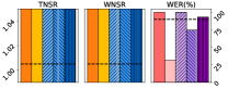
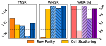
Attacks on Timing-driven Placement: In Fig. 9, the attack performance on timing-driven placement follows a similar trend as the wirelength-driven placement results in Fig. 8. ICMarks and ICMarks: GW remain resilient under all the removal attacks with a WER over 90%. Row Parity [20, 19] is also resilient to the attacks and has WER of over 90%. However, the watermarked layouts degrade the timing metrics (TNSR and WNSR) by 1% in Table V for timing-driven placement. The signatures in the baseline Cell Scattering [5] and ICMarks:DW are removed with WER 90%.
VI-2 Watermark Forging Attack
Instead of removing the watermarked signature, the adversary in a watermark forging attack counterfeits another set of watermarks on the watermarked layout and falsely claims his ownership. Row Parity [20, 19] and Buffer Insertion [6] techniques are not resilient to forging attacks. If the adversary has prior knowledge of the watermarking algorithm, they can easily counterfeit a different set of forged signatures from the row index ID of cells or add additional buffers into the layout for false ownership proof. For Cell Scattering [5], signatures are harder to counterfeit because forging the signature requires both random seeds and a non-watermarked layout. However, the inserted signatures can be easily erased by different watermark removal techniques in Section VI-1.
ICMarks: GW is resilient to forging attacks because the region with the minimal evaluation score is unique to the original non-watermarked placement. The non-watermarked layout and the scoring parameters are kept confidential. The ICMarks: GW signature verification requires the owner to provide that information to reproduce the watermark region . Therefore, the adversary cannot counterfeit the watermarks without access to the non-watermark layout. ICMarks: DW also exhibits similar properties, where the signatures are encoded before detailed placement on the intermediate placement . As such, the adversary with only access to the watermarked layout cannot reproduce the watermarked cells or distance to forge the signature. ICMarks, as a combination of ICMarks: GW and ICMarks: DW is also resilient to watermark forging attacks.
VII Conclusion
We present ICMarks, a robust watermarking framework for integrated circuits physical design IP protection in the supply chain. We first introduce a Global Watermarking method that identifies the watermarked region with insignificant performance degradation; then, we propose an independent Detailed Watermarking technique to select cells that do not overlap with neighbors after perturbation to encode watermarks. Based on these methods, we develop ICMarks, which combines the best attributes of both Global and Detailed Watermarking, thereby achieving minimal quality degradation with augmented robustness. Extensive experiments on ISPD’2015 [26], ISPD’2019 [27], and ICCAD’2015 [28] benchmarks demonstrate that ICMarks successfully inserts watermarks without compromising layout quality. Furthermore, we showcased ICMarks’s resiliency against watermark removal and forging attacks through comprehensive attack evaluations.
References
- [1] B. Liu and G. Qu, “VLSI supply chain security risks and mitigation techniques: A survey,” Integration, vol. 55, pp. 438–448, 2016.
- [2] L. Pawar, R. Kumar, and A. Sharma, “Risks analysis and mitigation technique in eda sector: VLSI supply chain,” in Analyzing the Role of Risk Mitigation and Monitoring in Software Development. IGI Global, 2018, pp. 256–265.
- [3] A. Cui, C.-H. Chang, and L. Zhang, “A hybrid watermarking scheme for sequential functions,” in 2011 IEEE International Symposium of Circuits and Systems (ISCAS), 2011, pp. 2333–2336.
- [4] D. Divyanshu, R. Kumar, D. Khan, S. Amara, and Y. Massoud, “Fsm inspired unconventional hardware watermark using field-assisted sot-mtj,” IEEE Access, vol. 11, pp. 8150–8158, 2023.
- [5] X. Cai, Z. Gao, F. Bai, and Y. Xu, “A watermarking technique for hard ip protection in post-layout design level,” in 2007 7th International Conference on ASIC, 2007, pp. 1317–1320.
- [6] G. Sun, Z. Gao, and Y. Xu, “A watermarking system for ip protection by buffer insertion technique,” in 7th International Symposium on Quality Electronic Design (ISQED’06). IEEE, 2006, pp. 5–pp.
- [7] D. Saha and S. Sur-Kolay, “Watermarking in hard intellectual property for pre-fab and post-fab verification,” IEEE Transactions on Very Large Scale Integration (VLSI) Systems, vol. 23, no. 5, pp. 801–809, 2014.
- [8] K. Shamsi, M. Li, K. Plaks, S. Fazzari, D. Z. Pan, and Y. Jin, “Ip protection and supply chain security through logic obfuscation: A systematic overview,” ACM Transactions on Design Automation of Electronic Systems (TODAES), vol. 24, no. 6, pp. 1–36, 2019.
- [9] J. Knechtel, S. Patnaik, and O. Sinanoglu, “Protect your chip design intellectual property: An overview,” in Proceedings of the International Conference on Omni-Layer Intelligent Systems, 2019, pp. 211–216.
- [10] P. SLPSK, S. Ray, and S. Bhunia, “Treehouse: A secure asset management infrastructure for protecting 3dic designs,” IEEE Transactions on Computers, 2023.
- [11] S. Sutardja, “1.2 the future of ic design innovation,” in 2015 IEEE International Solid-State Circuits Conference-(ISSCC) Digest of Technical Papers. IEEE, 2015, pp. 1–6.
- [12] M. Rostami, F. Koushanfar, and R. Karri, “A primer on hardware security: Models, methods, and metrics,” Proceedings of the IEEE, vol. 102, no. 8, pp. 1283–1295, 2014.
- [13] M. Rathor and G. P. Rathor, “Hard-sign: A hardware watermarking scheme using dated handwritten signature,” IEEE Design & Test, 2023.
- [14] H. Chen, C. Fu, B. D. Rouhani, J. Zhao, and F. Koushanfar, “Intellectual property protection of deep learning systems via hardware/software co-design,” IEEE Design & Test, 2023.
- [15] A. Tauhid, L. Xu, M. Rahman, and E. Tomai, “A survey on security analysis of machine learning-oriented hardware and software intellectual property,” High-Confidence Computing, p. 100114, 2023.
- [16] D. Saha, P. Dasgupta, S. Sur-Kolay, and S. Sen-Sarma, “A novel scheme for encoding and watermark embedding in vlsi physical design for ip protection,” in 2007 International Conference on Computing: Theory and Applications (ICCTA’07). IEEE, 2007, pp. 111–116.
- [17] F. Bai, Z. Gao, Y. Xu, and X. Cai, “A watermarking technique for hard ip protection in full-custom ic design,” in 2007 International Conference on Communications, Circuits and Systems. IEEE, 2007, pp. 1177–1180.
- [18] M. Ni and Z. Gao, “Watermarking system for ic design ip protection,” in 2004 International Conference on Communications, Circuits and Systems (IEEE Cat. No. 04EX914), vol. 2. IEEE, 2004, pp. 1186–1190.
- [19] A. B. Kahng, J. Lach, W. H. Mangione-Smith, S. Mantik, I. L. Markov, M. Potkonjak, P. Tucker, H. Wang, and G. Wolfe, “Constraint-based watermarking techniques for design ip protection,” IEEE Transactions on Computer-Aided Design of Integrated Circuits and Systems, vol. 20, no. 10, pp. 1236–1252, 2001.
- [20] A. B. Kahng, S. Mantik, I. L. Markov, M. Potkonjak, P. Tucker, H. Wang, and G. Wolfe, “Robust ip watermarking methodologies for physical design,” in Proceedings of the 35th annual Design Automation Conference, 1998, pp. 782–787.
- [21] T. Nie, T. Kisaka, and M. Toyonaga, “A watermarking system for ip protection by a post layout incremental router,” in Proceedings of the 42nd annual Design Automation Conference, 2005, pp. 218–221.
- [22] A. E. Dunlop, B. W. Kernighan et al., “A procedure for placement of standard cell VLSI circuits,” IEEE Transactions on Computer-Aided Design, vol. 4, no. 1, pp. 92–98, 1985.
- [23] R.-S. Tsay and E. Kuh, “A unified approach to partitioning and placement (VLSI layout),” IEEE Transactions on Circuits and Systems, vol. 38, no. 5, pp. 521–533, 1991.
- [24] R. S. Rajarathnam, Y. Lin, Y. Jin, and D. Z. Pan, “Regds: A reverse engineering framework from gdsii to gate-level netlist,” in 2020 IEEE International Symposium on Hardware Oriented Security and Trust (HOST), 2020, pp. 154–163.
- [25] L. Alrahis, A. Sengupta, J. Knechtel, S. Patnaik, H. Saleh, B. Mohammad, M. Al-Qutayri, and O. Sinanoglu, “Gnn-re: Graph neural networks for reverse engineering of gate-level netlists,” IEEE Transactions on Computer-Aided Design of Integrated Circuits and Systems, vol. 41, no. 8, pp. 2435–2448, 2021.
- [26] I. S. Bustany, D. Chinnery, J. R. Shinnerl, and V. Yutsis, “ISPD 2015 benchmarks with fence regions and routing blockages for detailed-routing-driven placement,” in Proceedings of the 2015 Symposium on International Symposium on Physical Design, 2015, pp. 157–164.
- [27] W.-H. Liu, S. Mantik, W.-K. Chow, Y. Ding, A. Farshidi, and G. Posser, “ISPD 2019 initial detailed routing contest and benchmark with advanced routing rules,” in Proceedings of the 2019 International Symposium on Physical Design, 2019, pp. 147–151.
- [28] M.-C. Kim, J. Hu, J. Li, and N. Viswanathan, “Iccad-2015 cad contest in incremental timing-driven placement and benchmark suite,” in 2015 IEEE/ACM International Conference on Computer-Aided Design (ICCAD), 2015, pp. 921–926.
- [29] Y. Qiu, Y. Xing, X. Zheng, P. Gao, S. Cai, and X. Xiong, “Progress of placement optimization for accelerating vlsi physical design,” Electronics, vol. 12, no. 2, p. 337, 2023.
- [30] S. Pawanekar, G. Trivedi, and K. Kapoor, “A nonlinear analytical optimization method for standard cell placement of vlsi circuits,” in 2015 28th International Conference on VLSI Design. IEEE, 2015, pp. 423–428.
- [31] A. Agnesina, K. Chang, and S. K. Lim, “VLSI placement parameter optimization using deep reinforcement learning,” in Proceedings of the 39th International Conference on Computer-Aided Design, 2020, pp. 1–9.
- [32] J.-M. Lin, C.-W. Huang, L.-C. Zane, M.-C. Tsai, C.-L. Lin, and C.-F. Tsai, “Routability-driven global placer target on removing global and local congestion for VLSI designs,” in 2021 IEEE/ACM International Conference On Computer Aided Design (ICCAD). IEEE, 2021, pp. 1–8.
- [33] Y. Lin, S. Dhar, W. Li, H. Ren, B. Khailany, and D. Z. Pan, “DREAMPlace: Deep learning toolkit-enabled gpu acceleration for modern vlsi placement,” in Proceedings of the 56th Annual Design Automation Conference 2019, 2019, pp. 1–6.
- [34] P. Liao, S. Liu, Z. Chen, W. Lv, Y. Lin, and B. Yu, “Dreamplace 4.0: Timing-driven global placement with momentum-based net weighting,” pp. 939–944, 2022.
- [35] P. Spindler, U. Schlichtmann, and F. M. Johannes, “Abacus: Fast legalization of standard cell circuits with minimal movement,” in Proceedings of the 2008 international symposium on Physical design, 2008, pp. 47–53.
- [36] R. Netto, S. Fabre, T. A. Fontana, V. Livramento, L. L. Pilla, L. Behjat, and J. L. Güntzel, “Algorithm selection framework for legalization using deep convolutional neural networks and transfer learning,” IEEE Transactions on Computer-Aided Design of Integrated Circuits and Systems, vol. 41, no. 5, pp. 1481–1494, 2021.
- [37] H. Yang, K. Fung, Y. Zhao, Y. Lin, and B. Yu, “Mixed-cell-height legalization on cpu-gpu heterogeneous systems,” in 2022 Design, Automation & Test in Europe Conference & Exhibition (DATE). IEEE, 2022, pp. 784–789.
- [38] M. Pan, N. Viswanathan, and C. Chu, “An efficient and effective detailed placement algorithm,” in ICCAD-2005. IEEE/ACM International Conference on Computer-Aided Design, 2005. IEEE, 2005, pp. 48–55.
- [39] W.-K. Chow, J. Kuang, X. He, W. Cai, and E. F. Young, “Cell density-driven detailed placement with displacement constraint,” in Proceedings of the 2014 on International symposium on physical design, 2014, pp. 3–10.
- [40] G. T. Becker, M. Kasper, A. Moradi, and C. Paar, “Side-channel based watermarks for integrated circuits,” in 2010 IEEE International Symposium on Hardware-Oriented Security and Trust (HOST). IEEE, 2010, pp. 30–35.
- [41] U. Das, M. S. Rahman, N. N. Anandakumar, K. Z. Azar, F. Rahman, M. Tehranipoor, and F. Farahmandi, “Psc-watermark: Power side channel based ip watermarking using clock gates,” in 2023 IEEE European Test Symposium (ETS). IEEE, 2023, pp. 1–6.
- [42] M. Shayan, K. Basu, and R. Karri, “Hardware trojans inspired ip watermarks,” IEEE Design & Test, vol. 36, no. 6, pp. 72–79, 2019.
- [43] A. Sengupta, M. Nabeel, N. Limaye, M. Ashraf, and O. Sinanoglu, “Truly stripping functionality for logic locking: A fault-based perspective,” IEEE Transactions on Computer-Aided Design of Integrated Circuits and Systems, vol. 39, no. 12, pp. 4439–4452, 2020.
- [44] H. M. Kamali, K. Z. Azar, F. Farahmandi, and M. Tehranipoor, “Advances in logic locking: Past, present, and prospects,” Cryptology ePrint Archive, 2022.
- [45] P. Santikellur, R. S. Chakraborty, and S. Bhunia, “Hardware ip protection using register transfer level locking and obfuscation of control and data flow,” in Behavioral Synthesis for Hardware Security. Springer, 2021, pp. 57–69.
- [46] P. Bagul, V. Inamdar et al., “Hardware obfuscation based watermarking technique for ipr ownership identification,” International Journal of Reconfigurable Computing, vol. 2023, 2023.
- [47] J. Gu, Z. Jiang, Y. Lin, and D. Z. Pan, “DREAMPlace 3.0: Multi-electrostatics based robust VLSI placement with region constraints,” in Proceedings of the 39th International Conference on Computer-Aided Design, 2020, pp. 1–9.
- [48] J. O. Berger and T. Sellke, “Testing a point null hypothesis: The irreconcilability of p values and evidence,” Journal of the American statistical Association, vol. 82, no. 397, pp. 112–122, 1987.
- [49] J. Lu, P. Chen, C.-C. Chang, L. Sha, D. J.-H. Huang, C.-C. Teng, and C.-K. Cheng, “eplace: Electrostatics-based placement using fast fourier transform and nesterov’s method,” ACM Transactions on Design Automation of Electronic Systems (TODAES), vol. 20, no. 2, pp. 1–34, 2015.
- [50] C.-K. Cheng, A. B. Kahng, I. Kang, and L. Wang, “Replace: Advancing solution quality and routability validation in global placement,” IEEE Transactions on Computer-Aided Design of Integrated Circuits and Systems, vol. 38, no. 9, pp. 1717–1730, 2018.
- [51] J. Liu, C.-W. Pui, F. Wang, and E. F. Y. Young, “Cugr: Detailed-routability-driven 3d global routing with probabilistic resource model,” in 2020 57th ACM/IEEE Design Automation Conference (DAC), 2020, pp. 1–6.
- [52] T.-W. Huang, G. Guo, C.-X. Lin, and M. D. Wong, “Opentimer v2: A new parallel incremental timing analysis engine,” IEEE transactions on computer-aided design of integrated circuits and systems, vol. 40, no. 4, pp. 776–789, 2020.
- [53] D. Saha and S. Sur-Kolay, “Fast robust intellectual property protection for vlsi physical design,” in 10th International Conference on Information Technology (ICIT 2007). IEEE, 2007, pp. 1–6.
- [54] W. Liang, X. Sun, Z. Xia, D. Sun, and J. Long, “A chaotic ip watermarking in physical layout level based on fpga,” Radioengineering, vol. 20, no. 1, pp. 118–125, 2011.
- [55] J. D. Lawson and Y. Lim, “The geometric mean, matrices, metrics, and more,” The American Mathematical Monthly, vol. 108, no. 9, pp. 797–812, 2001.
- [56] D. R. Anderson, K. P. Burnham, and W. L. Thompson, “Null hypothesis testing: problems, prevalence, and an alternative,” The journal of wildlife management, pp. 912–923, 2000.
- [57] C.-C. Huang, H.-Y. Lee, B.-Q. Lin, S.-W. Yang, C.-H. Chang, S.-T. Chen, Y.-W. Chang, T.-C. Chen, and I. Bustany, “Ntuplace4dr: A detailed-routing-driven placer for mixed-size circuit designs with technology and region constraints,” IEEE Transactions on Computer-Aided Design of Integrated Circuits and Systems, vol. 37, no. 3, pp. 669–681, 2018.