Large spontaneous valley polarization and anomalous valley Hall effect in antiferromagnetic monolayer
Abstract
Superior to ferromagnetic (FM) materials, antiferromagnetic (AFM) materials do not have any net magnetic moment and are robust to external magnetic perturbation with ultra-high dynamic speed. To achieve spontaneous valley polarization and anomalous valley Hall effect (AVHE) in AFM materials is of great significance for potential applications in spintronics and valleytronics. Here, we predict an A-type AFM monolayer with large spontaneous valley polarization. Monolayer has zero Berry curvature in momentum space but non-zero layer-locked hidden Berry curvature in real space, which provides the basic conditions for the realization of AVHE. Because possesses the combined symmetry ( symmetry) of spatial inversion () and time reversal () symmetry, the spin is degenerate, which prevents the AVHE. An out-of-plane external electric field can be used to produce spin splitting due to the introduction of layer-dependent electrostatic potential, and then layer-locked AVHE can be realized in . Moreover, the spin order of spin splitting can be reversed, when the direction of electric field is reversed. It is proved that the AVHE can be achieved in Janus without external electric field due to intrinsic built-in electric field. Our works provide an AFM monolayer with excellent properties to realize AVHE.
I Introduction
The valley is defined as the energy extrema of conduction and/or valence bands in momentum space, which is regarded as a degree of freedom in analogy to charge and spin. The valley index could be used for processing information and performing logic operations with low power consumption and high speed, known as the concept of valleytronicsq1 ; q2 ; q3 ; q4 . The rise of two-dimensional (2D) materials provides unprecedented opportunities for valley-relevant physics, and the significant advancements have been madeq1 ; q2 ; q3 ; q4 . As the typical valleytronic materials, the transition-metal dichalcogenide (TMD) monolayers possess a pair of degenerate but inequivalent -K and K valleys in the reciprocal space, which exhibit opposite Berry curvature and selective absorption of chiral lightq8-1 ; q8-2 ; q8-3 ; q9-1 ; q9-2 ; q9-3 . When the spin-orbit coupling (SOC) is considered, the -K and K valleys show opposite spin splitting, which can be called spin-valley locking. Unfortunately, the spontaneous valley polarization disappears in these nonmagnetic TMD monolayers, hindering further extension of valleytronics. Some extrinsic methods have been used to achieve valley splitting, such as external magnetic field, proximity effect, light excitationv5 ; v7 ; v9 ; v10 ; v11 .
The ferrovalley semiconductor (FVS) with intrinsic valley polarization has been proposedq10 , which spurs the continued advancement of valleytronicsq11 ; q12 ; q13 ; q13-1 ; q14 ; q14-1 ; q14-2 ; q15 ; q16 ; q17 ; q18 . The FVS is generally a hexagonal ferromagnetic (FM) monolayer with broken spatial inversion symmetry (), which can be used to achieve the anomalous valley Hall effect (AVHE). Compared to FM materials, the antiferromagnetic (AFM) materials possess the high storage density, robustness against external magnetic field, and ultrafast writing speedv12 . Therefore, realizing valley polarization and AVHE in AFM materials is more meaningful for energy-efficient and ultrafast valleytronic devices. A large number of AFM materials with spontaneous valley polarization are built on bilayer, which is constructed using the ferrovalley monolayer via van der Waals (vdW) interactionavh1 ; avh2 ; avh3 ; avh4 ; avh5 ; avh6 . In these AFM bilayers, the AVHE can be achieved, and the spin splitting can be induced by sliding ferroelectric polarization.
It may be more interesting to search for monolayer AFM materials to achieve spontaneous valley polarization and AVHE. For hexagonal AFM monolayer, the spontaneous valley polarization can appear, when including SOC. However, due to the absence of spin splitting in the band structures, the AVHE is prevented. The spin splitting in AFM materials can be produced by making the magnetic atoms with opposite spin polarization locating in the different environment (surrounding atomic arrangement)gsd . For example, the nonuniform potential caused by stacking AFM monolayer or on ferroelectric monolayer and constructing AFM Janus (X, Y=S, Se Te; XY) monolayers produces spin splitting in these AFM monolayers, and then the AVHE can be achievedv13 ; v14 ; v15 . The introduction of layer-dependent electrostatic potential caused by out-of-plane external electric field can also induce spin splitting in A-type AFM hexagonal monolayer and tetragonal monolayer , and the spin order of spin splitting can be reversed, when flipping the direction of electric fieldgsd1 ; gsd2 .
For A-type AFM hexagonal monolayer , the biaxial strain need be applied to change its valence band maximum (VBM) from to -K or K point, and the valley splitting is about 49 meVgsd1 . Only out-of-plane magnetic orientation can produce spontaneous valley polarization in AFM hexagonal monolayer, and the calculated magnetic anisotropy energy (MAE) is 27/unit cellgsd1 . It is very important and meaningful to search for AFM hexagonal monolayer with intrinsic -K/K valley, large valley splitting and strong out-of-plane magnetic anisotropy. Recently, 2D A-type AFM (X = F, Cl) and Janus monolayers have been predicted with strong out-of-plane magnetic anisotropy and high Nel temperatureszj , which share the similar crystal structures with . In this work, we predict that and possess large spontaneous valley polarization, which can be used to achieve AVHE.
II Computational detail
The spin-polarized first-principles calculations are performed within density functional theory (DFT)1 by using the projector augmented-wave (PAW) method, as implemented in Vienna ab initio Simulation Package (VASP)pv1 ; pv2 ; pv3 . We use generalized gradient approximation of Perdew-Burke-Ernzerhof (PBE-GGA)pbe as the exchange-correlation functional with the kinetic energy cutoff of 500 eV, the total energy convergence criterion of eV and the force convergence criterion of 0.0001 . To account for the localized nature of Fe-3 orbitals, a Hubbard correction is used by the rotationally invariant approach proposed by Dudarev et aldu . In ref.zj , the linear response method has been used to determine the effective () values, and they are 4.26, 4.96, and 4.27 eV for , and Janus monolayers, which are also adopted in our works. The SOC is incorporated for investigation of valley splitting and MAE. A slab model with a vacuum thickness of more than 30 along direction is used to avoid interlayer interactions. A 21211 Monkhorst-Pack k-point meshes are used to sample the Brillouin zone (BZ) for calculating electronic structures. The Berry curvatures are obtained directly from the calculated wave functions based on Fukui’s methodbm , as implemented in the VASPBERRY codebm1 ; bm2 .
III Crystal structures and magnetic ground state
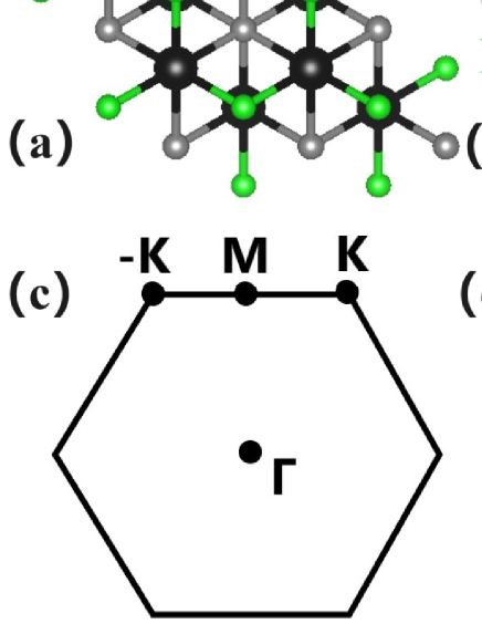
The crystal structures of along with the first BZ are shown in Figure 1 (a), (b) and (c), which consists of five atomic layers in the sequence of F-Fe-C-Fe-F, namely with the middle C layer sandwiched between two Fe-F bilayers. The crystallizes in the space group (No. 164), hosting spatial inversion symmetry without considering magnetic ordering. The magnetic ground state of can be determined by comparing the energies of FM and three AFM (AFM1, AFM2 and AFM3) configurations, as shown in Figure 1 (d). The AFM1 magnetic configuration of them is called A-type AFM state with the intralayer FM and interlayer AFM couplings. It is proved that the energy of AFM1 per unit cell is 651 meV, 15 meV and 395 meV lower than those of FM, AFM2 and AFM3 cases, confirming that the possesses A-type AFM ordeing. When spin is considered for , the inversion symmetry is missing for A-type AFM ordering, and the time-reversal symmetry is also lacking. However, a combination of inversion symmetry and time-reversal symmetry () exists in A-type AFM (see FIG.S1 of electronic supplementary information (ESI)). The optimized lattice constants are ==3.06 by GGA+ method, which is consistent with the previous value of 3.03 zj . The total magnetic moment of per unit cell is strictly 0.00 with the magnetic moment of bottom/top Fe atom being 3.91 /-3.91 .
IV Valley splitting and hidden Berry curvature
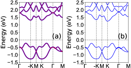
The energy band structures of are plotted in Figure 2 without SOC and with SOC for magnetization direction along the positive direction. Based on Figure 2 (a), the spin-up and spin-down channels are degenerate due to the symmetry, and the is an indirect band gap semiconductor with gap value of 1.54 eV. It is clearly seen that the energies of -K and K valleys in the conduction band are degenerate. The lattice of has inversion symmetry, but the opposite spin vectors of the two sublattices break spatial inversion () symmetry and time reversal () symmetry, giving rise to spontaneous valley polarization. The broken and can also be found in ferrovalley materials with spontaneous valley polarizationq10 . According to Figure 2 (b), when the SOC is included, the spin splitting is still absent, but the energy of -K valley becomes higher than one of K valley, producing valley polarization with valley splitting of 97 meV (). The valley splitting of is higher than those of available monolayer AFM valley materialsv13 ; v14 ; gsd1 ; gsd3 , and even higher than the valley splittings of many widely studied ferrovalley materialsq10 ; q11 ; q12 ; q13 ; q13-1 ; q14 ; q14-1 ; q14-2 ; q15 ; q16 ; q17 ; q18 . When including SOC, the is still an indirect band gap semiconductor, and the gap value is reduced to 1.47 eV.
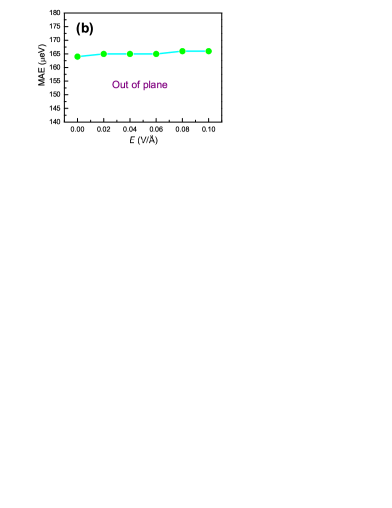
The symmetry of a system can be affected by different magnetic orientation, which has important effects on valley polarizationgsd4 ; gsd5 . For example, when the magnetic orientation is out-of-plane, the valley splitting can be observed for magnetic valley materials; while for in-plane magnetization, the spontaneous valley polarization will disappear. To achieve spontaneous valley polarization, an out-of-plane magnetic orientation is needed, and the MAE can be used to determine the magnetic orientation, which is defined as where and denote the in-plane and out-of-plane spin orientations. By GGA++SOC method, the calculated MAE is 164 /unit cell, and the positive value indicates the out-of-plane easy magnetization axis of . The out-of-plane easy magnetization axis confirms the spontaneous valley polarization of .
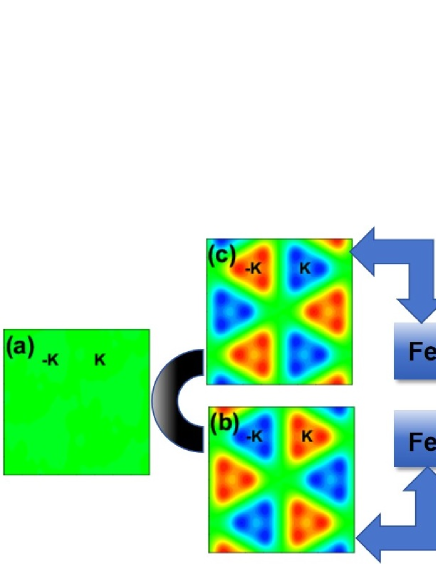
Due to symmetry of , there is zero berry curvature () everywhere in the momentum space. However, because each layer unit (F-Fe-C) breaks the local symmetry, there is layer-locked hidden Berry curvaturelqh . The A-type AFM ordering produces layer-spin locking, which makes the Berry curvatures of spin-up and spin-down channels equal in magnitude and opposite in sign. For , the distribution of Berry curvatures of total, spin-up and spin-down are shown in Figure 3. It is clearly seen that the total berry curvature everywhere in the momentum space is zero, and the hot spots of spin-resolved Berry curvatures locate at the -K and K valleys. The berry curvatures show opposite signs for different valley of the same spin channel and the same valley of different spin channel, producing layer-locked hidden Berry curvature in real space. By applying a longitudinal in-plane electric field, the Bloch carriers will acquire an anomalous transverse velocity q4 . When the Fermi level is shifted between the -K and K valleys in the conduction band, the spin-up and spin-down carriers from K valley will accumulate along opposite sides of different layer, resulting in the valley layer-spin Hall effect (FIG.S2 of ESI), but the AVHE is absent due to spin degeneracy.
V Spin splitting caused by electric field and AVHE
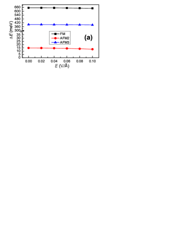
An out-of-plane electric field can be used to break the symmetry by removing symmetry of crystal structurex1 , and then the removal of spin degeneracy of -K and K valleys can be achieved. The layer-dependent electrostatic potential can be induced by an out-of-plane electric field, which leads to spin splitting effect. Here, an out-of-plane electric field (0.00-0.10 ) is applied, and the produces exactly the same results except spin order, which is because two Fe layers with opposite magnetic moments are related by a glide mirror symmetry. Within applied out-of-plane electric field, the magnetic ground state of is determined by calculating energy difference between FM/AFM2/AFM3 and AFM1 orderings. According to Figure 4 (a), A-type AFM ordering (AFM1 ordering) is always ground state within considered range, and the electric field has small influence on magnetic energy differences. The MAE vs is shown in Figure 4 (b), and the positive MAE confirms the out-of-plane magnetic orientation of within considered range. These ensure that the AVHE can be achieved in by electric field engineering.
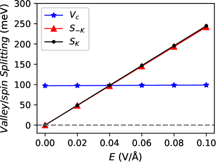
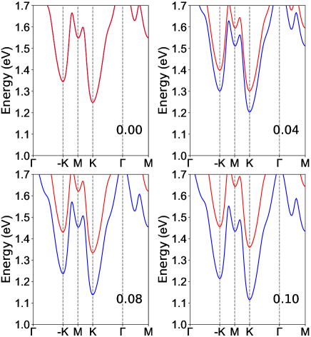
The energy band structures of at representative without SOC and with SOC are plotted in FIG.S3 of ESI, and the enlarged figures of spin-resolved SOC energy band structures near the Fermi level for the conduction band are plotted in Figure 5. With applied electric field, it is clearly seen that the spin degeneracy is removed. The valley splitting and spin splittings of -K and K valleys in the conduction band as a function of are shown in Figure 6. With increasing , the valley splitting increases from 97 meV to 99 meV, maintaining large spontaneous valley polarization. It is clearly seen that the spin splittings of -K and K valleys almost coincide, and show a linear relationship with . The out-of-plane electric field induces layer-dependent electrostatic potential rz , where and denote the electron charge and the distance of two Fe layers. The spin splittings of -K and K valleys can be estimated by . Taking =0.10 as a example, the estimated spin splitting is approximately 233 meV with the being 2.33 A, which is close to DFT result of 242 meV. With the electric field from to , the layer-dependent electrostatic potential is reversed, which makes spin order of spin splitting reverse, but the sizes of spin splitting and valley splitting remain unchanged (FIG.S4 of ESI).
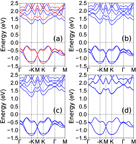
For at =0.10 , the energy band structures without SOC and with SOC for magnetization direction along the positive , negative , and positive direction are plotted in Figure 7. According to Figure 7 (a), the spin splitting can be observed due to the broken symmetry, and the energies of -K and K valleys in the conduction band are degenerate. Figure 7 (b) shows that the SOC can produce spontaneous valley polarization with valley splitting of 99 meV, and the energy of -K valley is higher than one of K valley. When the magnetization direction is reversed, the valley polarization can be switched with the same size of valley splitting(Figure 7 (c)), and the energy of K valley is higher than one of -K valley. When the magnetization direction of is in-plane along direction (Figure 7 (d)), no valley polarization and no obvious spin splitting can be observed. These similar magnetization-direction induced phenomena can also be observed in ferrovalley monolayersq11 ; q12 ; q13 ; q13-1 ; q14 ; q14-1 ; q14-2 ; q15 ; q16 ; q17 ; q18 .
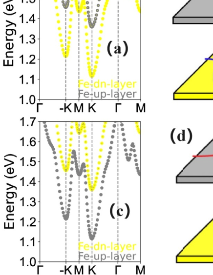
For at =0.10 , the distribution of Berry curvatures of total, spin-up and spin-down are plotted in FIG.S5 of ESI. Due to broken symmetry, the total nonzero berry curvature in the momentum space can be observed. It is clearly seen that the Berry curvatures show opposite sign for the same valley at different spin channel and different valley at the same spin channel. For monolayer , the Fe-layer-resolved conduction bands near the Fermi level with SOC at =+0.10 and -0.10 are plotted in Figure 8 (a) and Figure 8 (c). Under an in-plane electric field, when the Fermi level is shifted between the -K and K valleys in the conduction band, only the spin-up carriers from the K valley move to the boundary of bottom layer of the sample (Figure 8 (b)), producing layer-locked AVHE. Conversely, the spin-down carriers from the K valley will move to the opposite side of top layer of the sample (Figure 8 (d)), when the direction of electric field is reversed. This transverse accumulation of spin-polarized carriers can give rise to a net charge/spin current, and Figure 8 (b) and Figure 8 (d) generate opposite measurable voltage.
VI Spin splitting caused by Janus structure
The spontaneous valley polarization and electric-field induced spin splitting can also be achieved in (see FIG.S6 of ESI), but these valleys in the conduction band deviate from high symmetry -K/K point. For Janus monolayer, an out-of-plane intrinsic polar electric field can appear, which is equivalent to an external electric field for producing spin splittinggsd3 . By replacing the top F layer by Cl element in , the Janus monolayer is obtained (see Figure 9 (a) and (b)), which has the symmetry of (No. 156) without considering spin, lacking inversion symmetry . Calculated results show that the energy of AFM1 per unit cell is 648 meV, 15 meV and 373 meV lower than those of FM, AFM2 and AFM3 cases, confirming that the has A-type AFM ordering. When considering spin, the inversion symmetry and time-reversal symmetry are missing for A-type AFM , and a combination of inversion symmetry and time-reversal symmetry () also lacks. According to the the plane-averaged electrostatic potential along the direction, the built-in electric field of is predicted to be 1.71 (see FIG.S7 of ESI). In fact, Janus monolayer is an electric-potential-difference AFM materialgsd3 , which possesses spontaneous spin splitting.
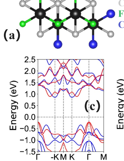
To confirm the spontaneous valley polarization of , the MAE is calculated, and the predicted value is 166/unit cell, which means that the easy magnetization axis of is out-of-plane. The energy band structures of are plotted in Figure 9 (c) and (d) without SOC and with SOC for magnetization direction along the positive direction. Due to the broken symmetry, the obvious spin splitting can be observed in , and it is an indirect band gap semiconductor without valley polarization (Figure 9 (c)). When considering the SOC, Figure 9 (d) shows spontaneous valley polarization with a valley splitting of 95 meV, which is larger than ones of many magnetic valley materialsv13 ; v14 ; gsd1 ; gsd3 ; q10 ; q11 ; q12 ; q13 ; q13-1 ; q14 ; q14-1 ; q14-2 ; q15 ; q16 ; q17 ; q18 . The total magnetic moment of per unit cell is strictly 0.00 , and the magnetic moment of bottom/top Fe atom is 3.82 /-3.90 .
For , the distribution of Berry curvatures of total, spin-up and spin-down are shown in FIG.S8 of ESI. Due to broken symmetry, shows the total nonzero berry curvature in the momentum space, and opposite sign for the same valley at different spin channel and different valley at the same spin channel. By shifting the Fermi level between the -K and K valleys in the conduction band, the spin-up carriers from K valley will accumulate along the bottom boundary of the sample under a longitudinal in-plane electric field, resulting in the layer-locked AVHE. Therefore, for Janus , the AVHE can be achieved without external electric field.
VII Conclusion
In summary, we present an A-type hexagonal AFM monolayer to realize AVHE by applying out-of-plane electric filed. The spontaneous valley polarization can occur in with the valley splitting of about 97 meV due to intrinsic the out-of-plane magnetic orientation, but the spin splittings of -K and K valleys are absent, preventing AVHE. The introduction of an out-of-plane electric field induces the spin splitting in monolayer , which is due to layer-dependent electrostatic potential. By combining with layer-locked hidden Berry curvature, the layer-locked AVHE can be achieved in monolayer by applying external electric field. Our works enrich valleytronic materials with AFM ordering, which provides advantageous for the development of energy-efficient and ultrafast electronic devices.
Acknowledgements.
This work is supported by Natural Science Basis Research Plan in Shaanxi Province of China (2021JM-456). We are grateful to Shanxi Supercomputing Center of China, and the calculations were performed on TianHe-2..References
- (1) J. R. Schaibley, H. Yu, G. Clark, P. Rivera, J. S. Ross, K. L. Seyler, W. Yao and X. Xu, Nat. Rev. Mater. 1, 16055 (2016).
- (2) G. Pacchioni, Nat. Rev. Mater. 5, 480 (2020).
- (3) S. A. Vitale, D. Nezich, J. O. Varghese, P. Kim, N. Gedik, P. Jarillo-Herrero, D. Xiao and M. Rothschild, Small 14, 1801483 (2018).
- (4) D. Xiao, M. C. Chang and Q. Niu, Rev. Mod. Phys. 82, 1959 (2010).
- (5) A. Srivastava, M. Sidler, A. V. Allain, D. S. Lembke, A. Kis and A. Imamoglu, Nat. Phys. 11, 141 (2015).
- (6) K. F. Mak, K. He, J. Shan and T. F. Heinz, Nat. Nanotechnol. 7, 494 (2012).
- (7) H. Zeng, J. Dai, W. Yao, D. Xiao, and X. Cui, Nat. Nanotechnol. 7, 490 (2012).
- (8) M. Zeng, Y. Xiao, J. Liu, K. Yang and L. Fu, Chem. Rev. 118, 6236 (2018).
- (9) C. Zhao, T. Norden, P. Zhang, P. Zhao, Y. Cheng, F. Sun, J. P. Parry, P. Taheri, J. Wang, Y. Yang, T. Scrace, K. Kang, S. Yang, G. Miao, R. Sabirianov, G. Kioseoglou, W. Huang, A. Petrou and H. Zeng, Nat. Nanotechnol. 12, 757 (2017).
- (10) D. MacNeill, C. Heikes, K. F. Mak, Z. Anderson, A. Kormnyos, V. Zlyomi, J. Park and D. C. Ralph, Phys. Rev. Lett. 114, 037401 (2015).
- (11) X. X. Zhang, Y. Lai, E. Dohner, S. Moon, T. Taniguchi, K. Watanabe, D. Smirnov and T. F. Heinz, Phys. Rev. Lett. 122, 127401 (2019).
- (12) L. Xu, M. Yang, L. Shen, J. Zhou, T. Zhu and Y. P. Feng, Phys. Rev. B 97, 041405 (2018).
- (13) W. Zhou, Z. Yang, A. Li, M. Long and F. Ouyang, Phys. Rev. B 101, 045113 (2020).
- (14) T. Cao, G. Wang, W. Han, H. Ye, C. Zhu, J. Shi, Q. Niu, P. Tan, E. Wang, B. Liu and J. Feng, Nat. Commun. 3, 887 (2012).
- (15) L. Xie and X. Cui, Proc. Natl. Acad. Sci. USA 113, 3746 (2016).
- (16) W. Y. Tong, S. J. Gong, X. Wan and C. G. Duan, Nat. Commun. 7, 13612 (2016).
- (17) Y. B. Liu, T. Zhang, K. Y. Dou, W. H. Du, R. Peng, Y. Dai, B. B. Huang, and Y. D. Ma, J. Phys. Chem. Lett. 12, 8341 (2021).
- (18) Z. Song, X. Sun, J. Zheng, F. Pan, Y. Hou, M.-H. Yung, J. Yang, and J. Lu, Nanoscale 10, 13986 (2018).
- (19) J. Zhou, Y. P. Feng, and L. Shen, Phys. Rev. B 102, 180407(R) (2020).
- (20) P. Zhao, Y. Ma, C. Lei, H. Wang, B. Huang, and Y. Dai, Appl. Phys. Lett. 115, 261605 (2019).
- (21) X. Y. Feng, X. L. Xu, Z. L. He, R. Peng, Y. Dai, B. B. Huang and Y. D. Ma, Phys. Rev. B 104, 075421 (2021)
- (22) S. D. Guo, J. X. Zhu, W. Q. Mu and B. G. Liu, Phys. Rev. B 104, 224428 (2021).
- (23) S. D. Guo, X. S. Guo, X. X Cai and B. G. Liu, Phys. Chem. Chem. Phys. 24, 715 (2022).
- (24) Y. Zang, Y. Ma, R. Peng, H. Wang, B. Huang, and Y. Dai, Nano Res. 14, 834 (2021).
- (25) R. Peng, Y. Ma, X. Xu, Z. He, B. Huang, and Y. Dai, Phys. Rev. B 102, 035412 (2020).
- (26) W. Du, Y. Ma, R. Peng, H. Wang, B. Huang, and Y. Dai, J. Mater. Chem. C 8, 13220 (2020).
- (27) R. Li, J. W. Jiang, W. B. Mi and H. L. Bai, Nanoscale 13, 14807 (2021).
- (28) T. Jungwirth, J. Sinova, A. Manchon, X. Marti, J. Wunderlich, and C. Felser, Nat. Phys. 14, 200 (2018).
- (29) T. Zhang, X. L. Xu, B. B. Huang, Y. Dai, L. Z. Kou and Y. D. Ma, Mater. Horiz. 10, 483 (2023).
- (30) Y. Liu, Y. Feng, Y. Dai, B. Huang and Y. Ma, Nano Lett. 24, 3507 (2024).
- (31) S. D. Guo, Y. L. Tao, G. Wang, S. Chen, D. Huang and Y. S. Ang, Front. Phys. 19, 23302 (2024).
- (32) W. Xun, C. Wu, H. Sun, W. Zhang, Y. Z. Wu and P. Li, Nano Lett. 24, 3541 (2024).
- (33) Y. Feng, J. Han, K. Zhang, X. Lin, G. Gao, Q. Yang and S. Meng, Phys. Rev. B 109, 085433 (2024).
- (34) Y. Feng, Y. Dai, B. Huang, L. Kou and Y. Ma, Nano Lett. 23, 5367 (2023).
- (35) S. D. Guo, Y. L. Tao, G. Wang and Y. S. Ang, J. Phys.: Condens. Matter 36, 215804 (2024).
- (36) T. Zhao, S. Xing, J. Zhou, N. Miao and Z. Sun, Journal of Materiomics 10, 269 (2024)..
- (37) W. Du, R. Peng, Z. He, Y. Dai, B. Huang, and Y. Ma, npj 2D Mater. Appl. 6, 11 (2022).
- (38) Y. Xu, H. Liu, Y. Dai, B. Huang and W. Wei, Appl. Phys. Lett. 122, 242404 (2023).
- (39) S. D. Guo, Y. L. Tao, Z. Y. Zhuo, G. Zhu and Y. S. Ang, Phys. Rev. B 109, 134402 (2024).
- (40) S. D. Guo, W. Xu, Y. Xue, G. Zhu and Y. S. Ang, Phys. Rev. B 109, 134426 (2024).
- (41) P. Wang, Q. Liu, N. Liu, M. Kuang, T. Yang, B. Wang, M. Ju, H. Yuan, X. Jiang and J. Zhao, ACS Appl. Mater. Interfaces 15, 52767 (2023).
- (42) P. Hohenberg and W. Kohn, Phys. Rev. 136, B864 (1964); W. Kohn and L. J. Sham, Phys. Rev. 140, A1133 (1965).
- (43) G. Kresse, J. Non-Cryst. Solids 193, 222 (1995).
- (44) G. Kresse and J. Furthmller, Comput. Mater. Sci. 6, 15 (1996).
- (45) G. Kresse and D. Joubert, Phys. Rev. B 59, 1758 (1999).
- (46) J. P. Perdew, K. Burke and M. Ernzerhof, Phys. Rev. Lett. 77, 3865 (1996).
- (47) S. L. Dudarev, G. A. Botton, S. Y. Savrasov, C. J. Humphreys, and A. P. Sutton, Phys. Rev. B 57, 1505 (1998).
- (48) T. Fukui, Y. Hatsugai and H. Suzuki, J. Phys. Soc. Japan. 74, 1674 (2005).
- (49) H. J. Kim, https://github.com/Infant83/VASPBERRY, (2018).
- (50) H. J. Kim, C. Li, J. Feng, J.-H. Cho, and Z. Zhang, Phys. Rev. B 93, 041404(R) (2016).
- (51) S. D. Guo and Y. S. Ang, Phys. Rev. B 108, L180403 (2023).
- (52) S. D. Guo, J. X. Zhu, M. Y. Yin and B. G. Liu, Phys. Rev. B 105, 104416 (2022).
- (53) S. D. Guo, W. Q. Mu and B. G. Liu, 2D Mater. 9, 035011 (2022).
- (54) R.Chen, H. P. Sun, M. Gu, C. B. Hua, Q. Liu, H. Z. Lu and X. C. Xie, Natl. Sci. Rev. 11, nwac140 (2024).
- (55) Y. Xue, W. Xu, B. Zhao, J. Zhang and Z. Yang, Phys. Rev. B 108, 075138 (2023).
- (56) R. W. Zhang, C. X. Cui, R. Z. Li, J. Y. Duan, L. Li, Z. M. Yu and Y. G. Yao, Preprint at https://doi.org/10.48550/arXiv.2306.08902 (2023).