Excitonic response in TMD heterostructures from first-principles: impact of stacking, twisting, and interlayer distance
Abstract
Van der Waals heterostructures of two-dimensional transition metal dichalcogenides provide a unique platform to engineer optoelectronic devices tuning their optical properties via stacking, twisting, or straining. Using ab initio Many-Body Perturbation Theory, we predict the electronic and optical (absorption and photoluminescence spectra) properties of MoS2/WS2 and MoSe2/WSe2 hetero-bilayers with different stacking and twisting. We analyse the valley splitting and optical transitions, and explain the enhancement or quenching of the inter- and intra-layer exciton states. Contrary to established models, that focus on transitions near the high-symmetry point K, our results include all possible transitions across the Brillouin Zone. This result, for a twisted Se-based heterostructures, in an interlayer exciton with significant electron density in both layers and a mixed intralayer exciton distributed over both MoSe2 and WSe2. We propose that it should be possible to produce an inverted order of the excitonic states in some MoSe2/WSe2 heterostructures, where the energy of the intralayer WSe2 exciton is lower than that in MoSe2. We predict the variability of the exciton peak positions (100 meV) and the exciton radiative lifetimes, from pico- to nano-seconds, and even micro-seconds in twisted bilayers. The control of exciton energies and lifetimes paves the way towards applications in quantum information technologies and optical sensing.
I Introduction
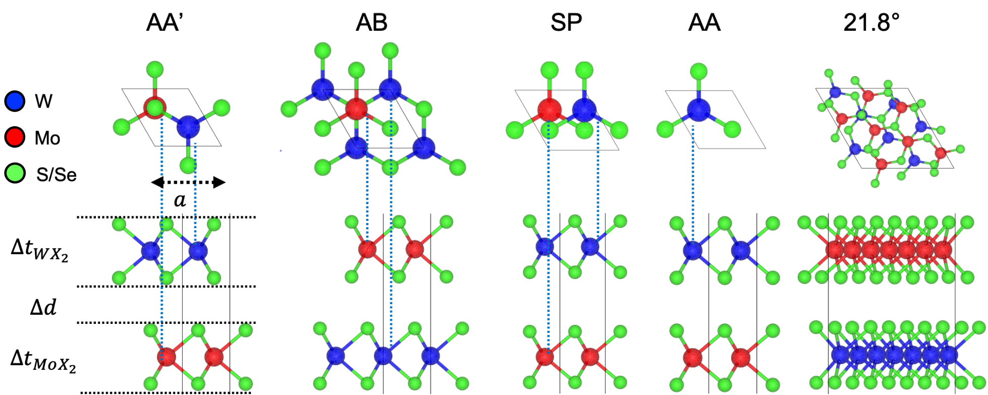
Transition metal dichalcogenides (TMDs) can host strong light-matter interaction and enhanced excitonic effects, making them ideal for next-generation optical devices [1]. TMD monolayers (MLs) can be further stacked into van der Waals heterostructures (vdW HS) [2, 3, 4] with added functionalities. Their electronic and optical properties strongly depend on layer thickness (), interlayer distance (), stacking and twist angle [5, 6, 7]. Achieving experimental control on these features is complex [8, 9]: encapsulation affects thickness and interlayer distance, and the dielectric environment influences transport and other properties. Thereofore, theoretical models are essential for isolating effects and guiding experimental design. In addition, for small twist angles, TMDs HS display regions which are misaligned and other with local atomic registry (AA′, AA, AB and SP, Fig. 1). In general, the changes of these degrees of freedom occur simultaneously. This makes it epxerimentally difficult to disentangle them.
Heterostructures of TMDs with different transition metal atoms typically show a type II band alignment, which leads to the formation of interlayer excitons (IL), in addition to intralayer (IN) ones [10]. Understanding how IN and IL exciton energies and intensities are affected by the above degrees of freedom is essential to control and exploit them for quantum information technologies [11, 12, 13]. The energetics, intensity and dynamics of bright IN excitons can be probed via photoluminescence (PL) or time-resolved photoluminescence (TRPL) [10, 14, 12]. Establishing a correspondence between observed peaks and individual monolayers is usually done by analogy with exciton energies in the freestanding MLs. However, this approach has limited predictive power as it neglects the vdW interaction between layers and the resulting electrostatic environment (screening). Ab initio Many-Body Perturbation Theory (Ai-MBPT) formalism, instead, allows for unambiguous identification of the spatial and spectral origin of each excitonic transition. The first ab-initio calculations of PL and absorption by IL and IN excitons in a TMD vdW HS were done by Torun et al [15], but with a focus on the AA′ stacking only. The same year Gillen et al. [16] computed absorption spectra of Se-based AA′, AA, AB HS using the Bethe-Salpeter Equation (BSE).
In this work, we systematically analyze the variation of the electronic and optical properties of MoX2/WX2 (with X = S/Se) vdW HS with interlayer distance, stacking and twisting, using Ai-MBPT [17, 18] We have updated the PL implementation in the Yambo code, following the general formalism of Melo and Marini [19] and incorporated the approaches and formalism developed in [20, 21]. These theories provide a framework for a full ab-initio description of the coupled out-of-equilibrium dynamics of photons, phonons, and electrons at different level of approximation. The dynamics of the carriers following light excitation can either be described in real-time or as a non-coherent thermalized exciton population. We implemented the computation of the lesser component of the electron-hole Green’s function, , which gives access to PL and transient absorption [18, 19]. We find that, under sufficient compression along the stacking direction, the excitonic ground state originates from an emerging transition at . This is due to enhanced orbital overlap in the vdW gap. In-plane compressive (resp. tensile) strain results in an increase (resp. decrease) of the first and second bright exciton energies. We predict that absorption and PL spectra can be unequivocally attributed to specific stacks/twists, as the corresponding shift of exciton energies are of the order of 100 meV. The absorption and PL spectra of twisted MoSe2/WSe2 heterostructures is particularly interesting as it hosts new emergent features: flat bands, an IL exciton with significant electron density contribution in both layers, two degenerate IN excitons localized on each of the ML, suppression of IN WSe2 exciton, and reversed excitonic order. The MoSe2/WSe2 twisted heterostructure is promising for applications in photovoltaics, as the computed exciton lifetimes reach 0.4 s, namely several order of magnitudes larger than typical values [22, 23].
II Theoretical Methods
The ground state properties are computed by solving the Kohn-Sham (KS) equations within the Density Functional Theory (DFT) formalism using the Quantum Espresso (QE) code [24, 25]. All structural relaxations were performed including Spin-Orbit Coupling (SOC), semi-empirical van der Waals correction D2 [26], and Se semicore states in the pseudopotential. The inclusion of Se semicore states is essential to predict the direct band-gap of MLs. Usually, the 3s and 3p Se states are assumed to be frozen in the core because of the large energy separation from 3d states. However, the spatial overlap of the corresponding wavefuntions is non-negligible. Freezing the semicore states results in an unphysical shift of the extrema of the conduction and valence bands, and indirect band-gap for both MoSe2 and WSe2 MLs phases (Appendix A).
In order to obtain quantitative predictions of the electronic structure, we computed corrections to DFT energies using the GW method [27] in the plasmon-pole approximation for all k-points in the Brillouin Zone (BZ) [28]. We employed the stochastic integration and the 2D cut-off of the Coulomb potential [29] to compute the screening . Neutral excitations are computed from the BSE for electron-hole interactions in the Ai-MBPT formalism [17, 18]. To obtain the exciton energies and wavefunctions, we solve the BSE in the Tamm-Dancoff approximation including local field effects [30]. The BSE can be recast into an eigenvalue equation
| (1) |
where are quasi-particle band energies, are the BSE coefficients and the energy of exciton . The optical absorption is computed from the imaginary part of the polarizability function , given by
| (2) |
where is the exciton response [18, 31] function and the thickness of the material. The PL spectra are computed as in [19], analogously to Ref.s [32, 15, 21, 20]. Here, we neglect the exciton-phonon coupling. In this approximation, the intensity of the emission spectra is
| (3) |
where, the minimum energy of the exciton dispersion, the refractive index, the exciton dipoles, a infinitesimally small imaginary number, and the Boltzmann constant We assume a low-density thermalized initial population of excitons. This can be modelled by a Bose distribution function, which parametrically depends on the exciton temperature [33, 34, 35, 15]. The excited state dynamics is described by the exciton radiative lifetimes in the optical limit () [22, 23]:
| (4) |
where is the area of the unit cell.
To visualize exciton wavefunctions () or identify IN or IL cases, one often chooses a “chemically reasonable” position for the hole (e.g. on the electrophilic chalcogen) and examines the electron part of . In the HS in particular, this choice is delicate and potentially arbitrary, e.g. which layer’s chalcogen should we choose? To analyse electron and hole localization within the heterostructure we define the probability P(IN) that a transition is intralayer using the integrals
| (5) |
where is the exciton wavefunction, and , denote electron and hole coordinates, respectively, with the coordinate normal to the heterostructure. The threshold is set halfway between the two layers. It follows that and give the interlayer transition probabilities. Their values are reported in Tables 8 and 9. The defined above is unequivocal in this sense and can distinguish IN and IL for each layer and in a quantitative fashion. The implementation of Eq. 4 and other post-processing to reproduce the main results of this work are available in the author’s forked repository of the Yambopy Python library111https://github.com/rreho/yambopy.
III Computational details
All calculations have been performed with fully relativistic pseudopotentials from PseudoDojo including the s, p and d semicore shells [37]. The ground state properties have been computed with Quantum Espresso [24] relaxing the structures with the Broyden (BFGS [38]) algorithm and the inclusion of spin orbit coupling and vdW corrections [26, 39], a plane wave kinetic energy cutoff of 120 Ry, and the PBE [40] exchange correlation functional. Atomic forces and pressure were converged to better than Ry/a.u. and kbar, respectively. With this choice, the total energies are converged to within less than 1 meV per unit cell.
The GW correction and excitonic properties have been computed on a 30x30x1 grid with 12 Å of vacuum for the MLs and 20 Å of vacuum for the HS. We employed the stochastic integration and the 2D cut-off of the Coulomb potential described in [29] to reduce the needed size of the reciprocal space grid. We included 500 unoccupied bands for the MLs, 900 for the S-based HS, 1200 for the Se-based aligned HS and 1600 for the twisted MoSe2/WSe2 in order to compute the screening and the BSE kernel. The values of the kinetic energy cut-off for the response functions and the exchange energy were convergenced to ensure precision better than 50 meV. Unless otherwise stated, we employed a K for the exciton population.
IV Results
IV.1 Ground state properties
All MLs and HS were fully relaxed (atoms and cell) with stresses and forces below kbar and Ry/a.u.. The lattice parameters (3.191 Å and 3.327 Å for S- and Se-based HS, respectively), remained unchanged in the other stackings. The most stable configuration is AA′, followed by AB, SP and AA (Table 1). In the AA stacking the metal atoms belonging to different MLs are on top of each other, resulting in electrostatic repulsion, increased total energy and increased interlayer distance . The layer thickness is not affected by the stacking (Table 4). During relaxation of the twisted Se-based HS, instead, the layer spacing shrinks significantly, resulting in enhanced pressure along the stacking direction and higher total energy.
| AA′ | AB | SP | AA | twisted | ||
|---|---|---|---|---|---|---|
| MoS2/WS2 | E | 0 | 3 | 21 | 75 | // |
| 3.040 | 3.026 | 3.523 | 3.633 | // | ||
| MoSe2/WSe2 | E | 0 | 4 | 26 | 105 | 980 |
| 3.137 | 3.138 | 2.253 | 3.721 | 2.954 |
IV.2 GW electronic band structure
A quantitative description of the electronic band structure allows one to determine the spatial origin of optical transitions and the direct/indirect nature of each system. This is especially important in phonon assisted processes where multiple electron scatterings might occur from K to Q and vice versa.
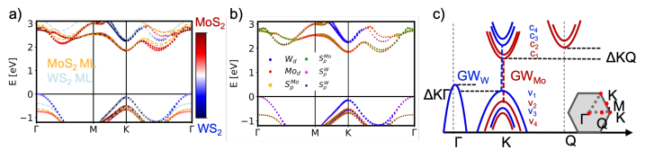
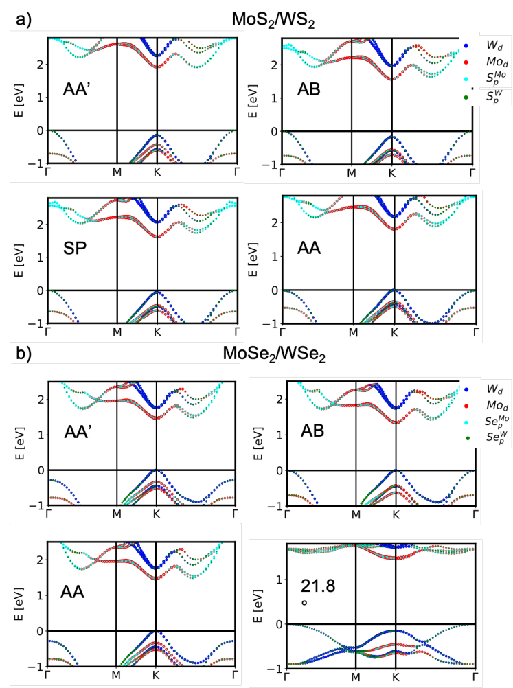
In Fig. 2 we analyse the GW band structure for the specific case of MoS2/WS2 in the AB stacking. All GW band structures are reported in Appendix C and Figures 7. The bands are projected either on layers (a), as schematically represented in (c), or on specific atomic orbitals (b). The orbital projection shows the effect of the MLs hybridization and screening in the HS. The HS band structure is more complex than a simple superposition of those of the constituent layers (orange and cyan dashed line in Fig. 2.a): the valence and conduction band edges display a type II alignment at K, with a reduced fundamental gap at K ( = 2.058 eV) with respect to the MLs, leading to the formation of IL excitons. The GW gap of TMD MLs and HS ranges between 1.2 – 2.5 eV and increases with the atomic number of the chalcogen atom, while it is less sensitive to the transition metal (Table 5).
The electronic states close to K either belong to WS2 or MoS2 layers (Fig. 2.a and c). Specifically, they belong to and orbitals of sulphur and metal atoms, respectively (Fig. 2.b). We denote , M = (Mo, W) the layer-specific GW gaps (topmost valence to lowest conduction band belonging to W/Mo). These determine the continuum energy level of IN excitons and their binding energy (BE). We predict that due to interlayer screening the gap in a vdW HS is considerably lower than the monolayer one, except for the AA′ MoS2/WS2 HS (Table 5 and Table 7).
All systems display a similar orbital projected band structure (Fig. 7) since they share the same crystal symmetry. The differences are due to the details of the stacking: The spatial overlap between out-of-plane and orbitals from each layer affects the valley splitting at high symmetry points of the conduction ( and valence () bands and the SOC splitting at K (Fig. 2.b). Going from the most stable (AA’) to the less stable (AA) structure, the energy overlap between the second and third valence band (involving and orbitals from both layers) increases ( Table 5), pushing upwards the valence band at the K point and resulting in a direct gap for the AA structure (). The Se-based HS exhibit direct gap, except for the twisted one. The variations in the band structure influence the IL and IN exciton energies; however, these are not the only determinants of the absorption peaks (see Section IV.3.b). The many-body Kernel, as described by Eq. 1, introduces additional complexity through screening effects that differ with each stacking configuration.
The computed GW gap of S-based HS agree with the literature within 10 meV, while the Se-based gaps are red-shifted by about 100 - 200 meV [3, 41, 42, 43, 44, 45]. This discrepancy is within the typical accuracy of GW/BSE simulations and can be attributed to specific simulation choices: relaxation with SOC, full Se semi-core pseudopotential, vdW correction, and use of the RIM-W 2D Coulomb potential integration method [29], which leads to increased screening with respect to previous simulations.
IV.3 Optical properties of HS
In this section, we present the absorption and emission spectra of vdW HS. In particular, we discuss the IL excitons and the change in their energy onset upon varying the interlayer distance . We distinguish between symmetry forbidden dark IL excitons and “grey” excitons, which are dark due to the reduced overlap between the hole and electron wavefunctions.
Spectra:
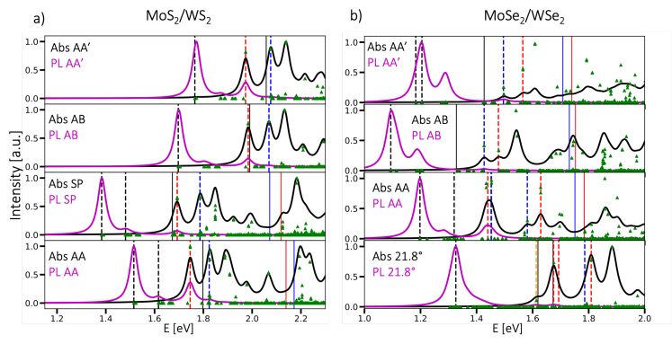
Fig. 3 shows the PL and absorption spectra (Eq. 2) for different HS stackings. For the three stacking that are closer in total energy (AA’, AB, SP), we predict a red-shift of the spectra. This is marked by the IL (black dashed lines, transition) and IN (red/blue dashed lines, and , respectively) excitons. The AA and twisted stackings exhibit quite a different structure (as indicated by the higher total energy) and cannot be directly compared to the above. The vdW HS bright exciton peaks (Table 2) are red shifted with respect to the constituent MLs (Table 6), except for the AA′ (stable) and AB stacking of the S-based HS. The BEs of the IN excitons are considerably smaller (100 meV) in the vdW HS Table 2 with respect to the MLs Table 6. Thus, it is not straightforward to determine the layer localization of HS excitons simply comparing with the MLs.
In the twisted HS the reduced interlayer distance and rotation compensate each other. As a consequence, exciton positions are close to those of the MLs. Moreover, the IN-W exciton around1.8 eV is quenched, and it shows a small oscillator strength. We expect this to be a result of the compression along the stacking direction.
The magnitude of the gaps varies among different stacking, the binding energy of the IL and IN excitons are close in magnitude (Table 2), again except for the twisted HS which has a larger binding energy. This implies that variations in the energy gaps and the contributions stemming from the many-body Kernel (as described in Eq. 1) counterbalance one another.
Interlayer excitons:
In all vdW HS (Fig. 3) we identify a dark IL exciton state below the first IN-Mo and IN-W peaks. Our results predict a reversed intralayer exciton order around 1.4 eV in the MoSe2/WSe2 AA′ and AB stacking , with the IN-W exciton lower in energy than IN-Mo. This unexpected reversed exciton order can be explained by the energy discrepancy in the electronic properties of the parent MLs (Section IV.2). Note that the exciton order is very sensitive to the details of the relaxation procedure.
The electron distribution of the IL exciton in TMD HS does not reside only in the vacuum region between the two layers, contrary to predictions based on continuum models. We understand this as a consequence of the nature of the exciton wavefunction, which formally contains contributions from all the -points in the Brillouin Zone. Such electron distribution cannot be described in models that compute the optical properties only in proximity to the high-symmetry point K.
Our results show that IL excitons of the twisted HS have a significant electron density weight in both layers (Table 9). Moreover, for the same system, we predict an exciton state just below the electronic gap, indicated in orange (Fig. 3.b), featuring mixed intralayer MoSe2 (v2-c2) and WSe2 (v1-c4) transitions. We label this state IN(Mo+W). Analogously, not all the IN excitons have an electronic distribution highly localized within one layer (Table 9 and 8). An example of this can be seen in the AB stacking of MoSe2/WSe2, where the probability of IN localization, denoted as P(IN-W) (Eq. 5), is only 20.21%.
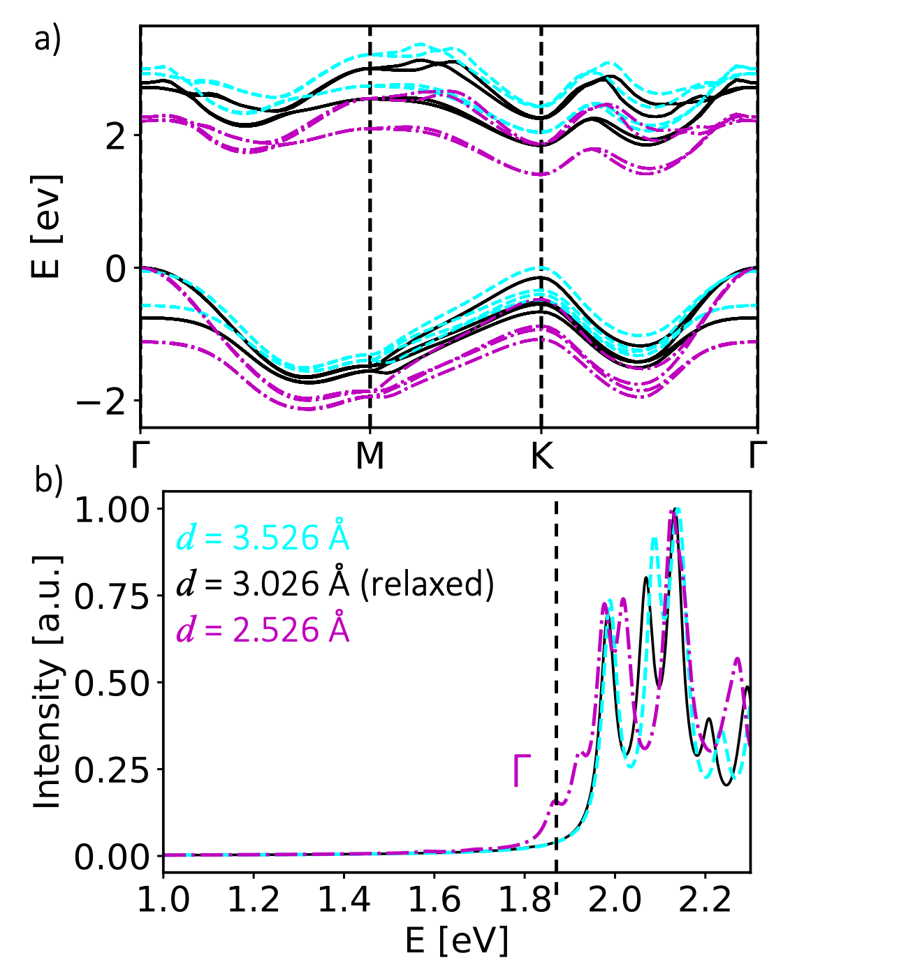
To assess the dependence of the exciton peaks on the interlayer distance , we consider the specific case of MoS2/WS2 in the AB stacking (Fig. 4). We varied by 0.5 Å and inspected the effects on the band structure and absorption. Increasing the bands blueshift by about 200 meV, but absorption peaks blueshift by only 6 meV. This implies that c-axis tensile strain has a relatively weak effect on the position of the peaks.
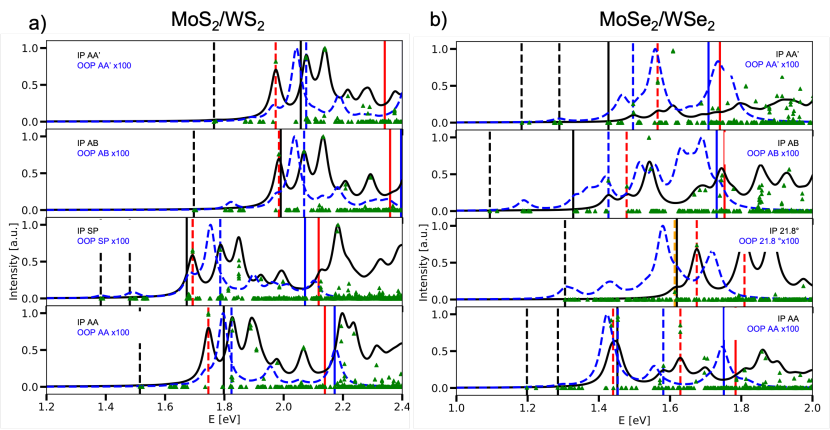
Decreasing the bands redshift by 400 meV, the system is in an unfavourable configuration with high stresses and pressure. Absorption changes drastically, with new peaks arising between 1.8 and 1.9 eV (Fig. 4.b). In particular, the enhanced overlap between the orbitals due to vertical compression results in a new bright transition at at 1.86 eV. The lack of inversion symmetry in vdW HS results in a 10 meV splitting of the c1/c2 bands. The effect of the splitting propagates to the absorption and emission spectra (Eq. 1) where the first poles of the BSE equation with low oscillator strength (green triangles Figs 3.a and 3.b) are IL excitons, with energy splitting of the order of the SOC splitting [46]. This effect is more pronounced in Se-based HS due to Se larger atomic mass and SOC. In addition, MoS2/WS2 in the SP stacking displays two dark IL exciton state groups separated by 0.098 eV. Se-based vdW HS, instead, display two distinct IL excitons in the AA′ and AA stacking. Furthermore, we observe that all systems have clusters of dark BSE equation poles below the first bright peak whose energy, shape, and spread varies with the different stacking.
dark and “grey” IL excitons:
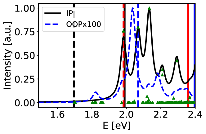
The darkness of excitons can be due to symmetry as in MLs but also to the interlayer nature, which implies very small overlap between the hole and electron wavefunctions. The latter excitons are “grey”, but not dipole forbidden. To discern the dark IL exciton, one can either inspect the dipole matrix elements or move the electric field polarization out of plane. Considering again the AB alignment of MoS2/WS2 as a prototypical example we see that varying the electric field direction, the forbidden IL exciton at 1.8 eV becomes bright, with the IN excitons being weaker than the in-plane (IP) configuration (Fig. 5). In particular, we observe that, among the series of IL excitons below the fundamental gap, the first one remains dark in the out-of-plane (OOP) configuration while the second one becomes bright. This is due to different spin indices of the bands involved in the formation of the exciton states. The first IL exciton of the series comes from a transition between (spin-down/spin-up), while the second one from (spin-down/spin-down). Note that in Fig. 5 we rescaled the maximum absorption to 1 for both IP and OOP configuration, however, in absolute value, the OOP one is around two orders of magnitude weaker due to the smaller out-of-plane dipole.
Detailed exciton energies and transitions for the various systems are listed in Table 2. In Appendix E we report the absorption plots for IP and OOP electric field direction for all systems, along with information on the relevant energetic transitions.
| System | Stacking | IX0 exciton | IX1 exciton | IX2 exciton | |||||||
|---|---|---|---|---|---|---|---|---|---|---|---|
| E [eV] | BE [eV] | IL/IN | E [eV] | BE [eV] | IL/IN | E [eV] | BE [eV] | IL/IN | |||
| MoS2/WS2 | AA′ | 1.765 | 0.292 | IL | 1.973 | 0.368 | IN-Mo | 2.075 | 0.327 | IN-W | |
| AB | 1.697 | 0.293 | IL | 1.984 | 0.375 | IN-Mo | 2.069 | 0.327 | IN-W | ||
| SP | 1.383 | 0.290 | IL | 1.693 | 0.379 | IN-Mo | 1.786 | 0.332 | IN-W | ||
| AA | 1.515 | 0.283 | IL | 1.746 | 0.393 | IN-Mo | 1.824 | 0.348 | IN-W | ||
| MoSe2/WSe2 | AA′ | 1.205 | 0.222 | IL | 1.496 | 0.204 | IN-W | 1.565 | 0.175 | IN-Mo | |
| AB | 1.094 | 0.235 | IL | 1.427 | 0.305 | IN-W | 1.478 | 0.275 | IN-Mo | ||
| AA | 1.198 | 0.252 | IL | 1.435 | 0.349 | IN-Mo | 1.581 | 0.170 | IN-W | ||
| 21.8∘ | 1.305 | 0.475 | IL | 1.613 | Mo: 0.430 W: 0.387 | IN-Mo and IN-W | 1.675 | 0.477 | IN-Mo | ||
V Photoluminescence and exciton radiative lifetimes
Photoluminescence gives a quantitative description of the states involved in the creation of the IL exciton and their recombination time which is crucial for any technological application, such as solar energy conversion devices [47, 48, 49, 50, 51].
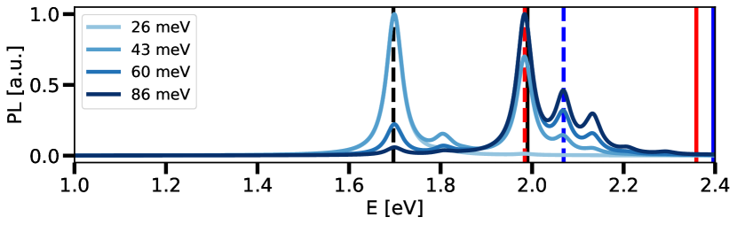
Exciton population is tuned by changing the (in K or meV) in the Bose distribution. For very small exciton population at K, the PL intensity peaks at the lowest dark exciton state. In emission, we see that higher exciton states are populated and emit from the energy positions of the BSE poles (Fig. 6).
Fixing the exciton temperature at 400 K, we inspect the information carried by the PL spectra among different stacking (Fig. 3). In analogy to the IP vs OOP electric field configuration described in Section IV.3, the emission spectra show that not all dark IL excitons are the same in nature. Again, we can distinguish between dark (spin forbidden) and “grey” (small electron/hole overlap) IL excitons. Interestingly, PL allows analyzing further the BSE poles and it carries complementary information with respect to the absorption spectra (both IP and OOP). Varying the direction of the electric field reveals the relative intensity of the exciton peaks in relation to the excitation direction. Meanwhile, PL serves as a distinct method for identifying the most prominent interlayer (IL) emission peaks beneath the fundamental gap, among the series of BSE poles. For example, in the AA′ stacking (both S- and Se- based HS) we have two BSE poles around 1.77/1.19 eV, but only the second one is bright in emission. The PL spectra for the Se-based 21.8∘ twisted HS is rather unique. IL excitons are not peaked at K but between and (see Supplementary Information). Note that, in addition to IL excitons, PL is peaked also for poles belonging to IN excitons.
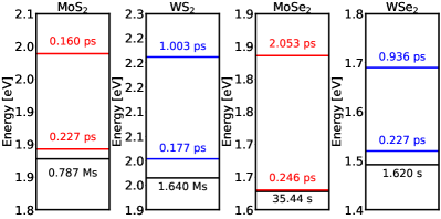
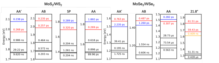
The exciton radiative lifetimes can be modulated extensively across several orders of magnitude by varying factors such as the number of layers, stacking configurations, and temperature [23, 22, 52, 53], as confirmed by our results illustrated in Fig. 11. Longer lifetimes are interesting, for instance, for photovoltaic applications [48].
In MLs, the dark exciton states are long-lived (1 Mega-second) attributable to the low exciton oscillator strength, suggesting a low probability of re-emission upon occupation (Appendix Fig. 10). Bright excitons possess lifetimes in the picosecond range, aligning with values reported in similar studies [22, 23]. In vdW HS we observe a significant change in the order of magnitude of the lifetimes depending on the stacking. The IL exciton lifetimes are in the pico/nanosecond range with a couple of exceptional transitions in the range for the AA stacking. The IN exciton lifetimes are all within the picosecond range, except for the mixed IN excitons of Se-based twisted vdW HS around 1.62 eV. Moreover, the stacking shows a long-lived ground state IL exciton with lifetime . The order of magnitude of the lifetime is inversely proportional to the exciton dipole strength (Eq. 4). IL excitons are characterized by an out-of-plane dipole moment. Its strength depends on the distance and especially on the overlap between the constituent electron and hole wave functions. A reduced overlap leads to a reduction of the exciton dipole strength and in turn an increase of its lifetime. The order of magnitude of these excitons radiative lifetimes aligns quite well with available experiments which report, for the IL exciton lifetime, a value of in MoS2/WS2 and ns in MoSe2/WSe2 [54, 55, 56, 57, 14]. To sum up, we show that there are IL excitons with ultra-long lifetime of the order of and that PL is a useful tool to identify stackings and investigate the nature of IL excitons in vdW HS.
VI Conclusion
We compute the electronic band structure, absorption spectra and photoluminescence for MoS2/WS2, MoSe2/WSe2 vdW heterostructures in different stacking configurations and compare to the constituent MLs. We discuss the shift and variations of the exciton peaks, order, and lifetimes with different stacking, and analyze the sensitivity of these results to the geometrical relaxation and the inclusion of semicore states in the pseudopotentials. We show that in vdW HS, the intralayer excitons have electron density spread in both layers. This feature is enhanced in the Se-based twisted HS where the mixed intralayer exciton has an electron density distributed over both MoSe2 and WSe2. In addition, the twisted HS has a peculiar IL exciton with the electron density spread in both layers. We discuss on the difference between spin-forbidden dark interlayer excitons and “grey” excitons, whose darkness is the result of a reduce spatial overlap between the electron and hole wavefunctions. We show that “grey“ excitons become bright when the dipoles are excited in the stacking direction. Furthermore, we show that the emission spectra obtained with our implementation of the PL spectra within the Ai-MBPT formalism in the Yambo code can bring additional insight into the nature of “grey” excitons.
Our findings highlight the potential to use absorption and emission as characterization tools for HS stacking. The tunability of the excitonic properties of vdW TMDs heterostructures promises significant applications in Quantum Information, especially in logical qubit creation.
Acknowledgements.
The authors acknowledge the fruitful discussion with Pedro M.M.C. de Melo, D. Vanmaekelbergh, M. Palummo, A. Marini and F. Paleari as well as extensive support from the Yambo developer team. RR, ABM and ZZ acknowledge financial support from “Materials for the Quantum Age - QuMat” project (registration number 024.005.006, Gravitation program of the Dutch Ministry of Education, Culture and Science OCW), and the European Union “Quondensate” project (Horizon EIC Pathfinder Open, grant agreement No. 101130384). MJV is supported by ARC project DREAMS (G.A. 21/25-11) funded by Federation Wallonie Bruxelles and ULiege, and the Excellence of Science (EOS) programme (grant 40007563-CONNECT) funded by the FWO and F.R.S.-FNRS. The results of this research have been achieved using supercomputer facilities provided by NWO - Domain Science (Snellius), the Tier-0 PRACE Research Infrastructure resource Discoverer based in Sofia, Bulgaria (OptoSpin project id. 2020225411) and Mare Nostrum by the Barcelona Supercomputing center (Spanish Supercomputing Network, RES).Appendix A The role of Se semi-core states and van der Waals correction
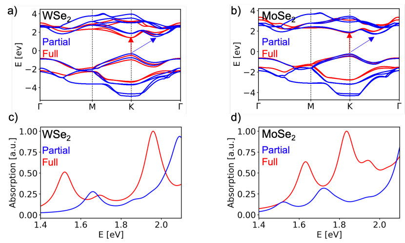
The treatment of the potential generated by the electronic states of Selenium (atomic number Z = 34) is critical for the assessment of the direct/indirect gap nature of TMDs MLs. In the pseudopotential approach, core electrons are considered to be frozen. If only partial Se semicore states are included in the pseudopotential we find an unphysical indirect GW band gap for the TMDs monolayers. Including semi-core states and relaxing the structure with van der Waals corrections provided the correct direct band structure. As an example, we provide a table of the relaxed lattice parameter for WSe2 using different pseudo-potentials, with/without van der Waals correction (Table 3). In Figure 8 we show these effects for the GW band structure of MoSe2 and WSe2. The shift in energy is also reflected in the position of the exciton peaks in absorption. Coincidentally, the position of the first exciton for WSe2 with partial semi-core pseudopotentials is 1.63 eV and closer to the experimental value than the one reported in the main text, 1.520 eV. Moreover, employing partial semi-core pseudopotentials the MoSe2 IX0 exciton (at 1.52 eV) is lower in energy than the WSe2 IX0 exciton. Since full semi-core pseudopotential lead to the correct band structure for the MLs, we employ full semi-core pseudopotentials throughout this study for consistency. We understand this difference as an increased screening due to the treatment of the Coulomb potential as a truncated potential in a slab geometry [29].
| a [Å] | [Å] | vdW | Semicore | gap [eV] | GW gap |
|---|---|---|---|---|---|
| 3.323 | 3.360 | No | Partial | 2.178 | Indirect |
| 3.323 | 3.360 | Yes | Partial | 2.253 | Indirect |
| 3.338 | 3.251 | Yes | Full | 1.934 | Direct |
Appendix B Structural properties of ML and HS
Relaxed structural parameters (lattice parameter , layer thickness and , and van der Waals gap ) of MLs and HS are reported in Table 4.
| System | Stacking | [Å] | [Å] | [Å] | [Å] |
|---|---|---|---|---|---|
| MoS2 | // | 3.194 | // | 3.129 | // |
| WS2 | // | 3.195 | // | // | 3.129 |
| MoSe2 | // | 3.317 | // | 3.301 | // |
| WSe2 | // | 3.338 | // | // | 3.251 |
| MoS2/WS2 | AA′ | 3.191 | 3.040 | 3.116 | 3.132 |
| AA | 3.191 | 3.633 | 3.117 | 3.131 | |
| AB | 3.191 | 3.026 | 3.116 | 3.130 | |
| SP | 3.191 | 3.523 | 3.116 | 3.131 | |
| MoSe2/WSe2 | AA′ | 3.327 | 3.137 | 3.329 | 3.342 |
| AA | 3.327 | 3.721 | 3.328 | 3.342 | |
| AB | 3.327 | 3.138 | 3.328 | 3.342 | |
| 21.8∘ | 8.780 | 2.954 | 3.280 | 3.333 |
Appendix C GW band structures for TMD HS
For each system, we report the orbital-projected band structure in Fig. 7. Our findings indicate that all systems exhibit a type II band alignment, with the primary composition of the first four conduction and valence bands being the d-orbitals of the metals and the p-orbital of the chalcogen atom. Although the orbital projections vary only slightly among the systems, the and splittings are strongly influenced by the different stacking configurations, as reported in the main text and in Table 5.
| System | stacking | |||||||||||
|---|---|---|---|---|---|---|---|---|---|---|---|---|
| MoS2/WS2 | AA′ | 2.058 | 2.341 | 2.403 | -0.150 | 0.000 | 0.283 | 0.142 | 0.033 | 0.008 | 0.336 | 0.015 |
| AB | 1.990 | 2.359 | 2.397 | -0.149 | 0.009 | 0.369 | 0.142 | 0.117 | 0.008 | 0.336 | 0.011 | |
| SP | 1.673 | 2.072 | 2.118 | -0.060 | 0.122 | 0.398 | 0.033 | 0.124 | 0.009 | 0.435 | 0.011 | |
| AA | 1.798 | 2.139 | 2.172 | 0.021 | 0.094 | 0.341 | 0.066 | 0.086 | 0.010 | 0.365 | 0.008 | |
| MoSe2/WSe2 | AA′ | 1.427 | 1.748 | 1.706 | 0.028 | 0.030 | 0.331 | 0.018 | 0.079 | 0.027 | 0.383 | 0.011 |
| AB | 1.329 | 1.753 | 1.731 | 0.006 | 0.090 | 0.424 | 0.018 | 0.183 | 0.019 | 0.383 | 0.025 | |
| AA | 1.452 | 1.784 | 1.751 | 0.281 | 0.030 | 0.331 | 0.113 | 0.079 | 0.027 | 0.272 | 0.011 | |
| 21.8∘ | 1.780 | 2.042 | 1.983 | -0.156 | 0.159 | 0.302 | 0.150 | 0.045 | 0.025 | 0.226 | 0.015 |
Appendix D Absorption and Emission Spectra of TMD Monolayers
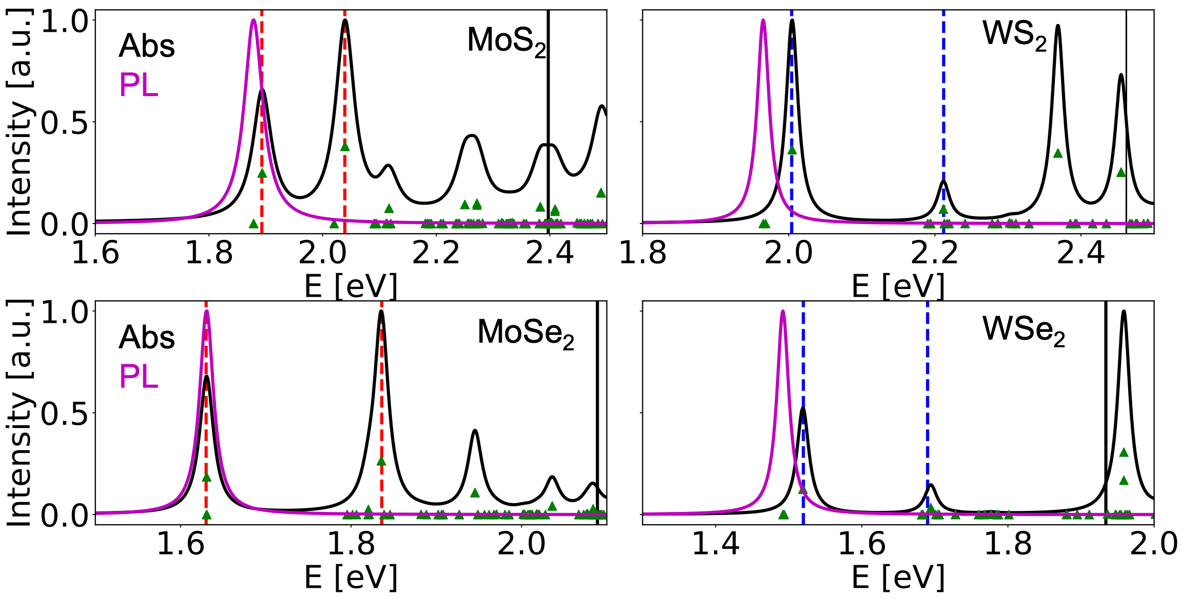
The absorption and emission spectra (Eq. 1 and Eq. 2) of the MLs (Fig. 9), confirm the high exciton binding energy attributed to diminished dielectric screening in the 2D limit. We observe a prominent emission peak at the first exciton eigenstate of the BSE Hamiltonian (Eq. 1). This peak coincides with the position of the first finite oscillator strength (green triangles) and is dark in absorption due to optical selection rules (spin forbidden). MoSe2 has a dark exciton degenerate with the first bright peak, confirming previous reports [10, 58]. The computed excitonic peaks (labelled as IXN, where ), align closely with experimental data for the S-based MLs [33] (Table 6). The results for Se-based MLs are further from experimental findings [59] (e.g. the energy of the first exciton peak in WSe2 is about 100-200 meV lower ) due to the underestimation of the electronic energy gap (Section IV.2).
| ML | IX1 [eV] | BE [eV] | IX2 [eV] | BE [eV] | PL [eV] |
|---|---|---|---|---|---|
| MoS2 | 1.893 | 0.504 | 2.039 | 0.358 | 1.878 |
| WS2 | 2.004 | 0.458 | 2.212 | 0.250 | 1.965 |
| MoSe2 | 1.630 | 0.459 | 1.836 | 0.253 | 1.630 |
| WSe2 | 1.520 | 0.414 | 1.694 | 0.240 | 1.492 |
| ML | gap [eV] | [eV] | [eV] |
|---|---|---|---|
| MoS2 | 2.397 | 0.122 | 0.184 |
| WS2 | 2.462 | 0.252 | 0.028 |
| MoSe2 | 2.089 | 0.345 | 0.144 |
| WSe2 | 1.934 | 0.312 | 0.309 |
Appendix E Optical absorption of TMD heterostructures
We report a detailed table with the most notable transitions in the BSE spectra that are visible either in absorption (IP and OOP) or PL in Table 10. Moreover, in Fig. 12, we visualize the IP and OOP absorption spectra for all studied systems. We observe that the most intense OOP peaks are all dark in the IP configuration, and the brightest IP peaks are reduced in the OOP configuration.
| stacking | [eV] | IX0 | P(IL) | IX1 | P(IN-Mo) | IX2 | P(IN-W) |
|---|---|---|---|---|---|---|---|
| AA’ | 1.960 | 1.670 (0.290) | 97.81% | 1.889 (0.366) | 94.06% | 2.057 (0.255) | 54.74% |
| AA | 1.798 | 1.515 (0.283) | 99.2% | 1.746 (0.393) | 99.7% | 1.824 (0.348) | 65.24% |
| AB | 1.727 | 1.194 (0.533) | 99.2% | 1.496 (0.618) | 98.3% | 1.639 (0.475) | 99.0% |
| SP | 1.673 | 1.383 (0.290) | 99.14% | 1.693 (0.379) | 80.15% | 1.786 (0.332) | 97.26% |
| stacking | [eV] | IX0 | P(IL) | IX1 | P(IN-) | IX2 | P(IN-) |
|---|---|---|---|---|---|---|---|
| AA’ | 1.427 | 1.205(0.222) | 97.70% | 1.496(0.204) | 57.91%(W) | 1.565(0.175) | 84.38% (Mo) |
| AA | 1.452 | 1.198(0.252) | 96.98% | 1.435(0.349) | 99.6%(Mo) | 1.581(0.170) | 59.06% (W) |
| AB | 1.329 | 1.094(0.235) | 98.71% | 1.427(0.3049) | 20.21%(W) | 1.478(0.275) | 86.16% (Mo) |
| 21.8∘ | 1.780 | 1.305(0.138) | 52.63% | 1.613(0.370/0.415) | 40.31%(W) | 1.675(0.477) | 25.63%(Mo) |
| MoS2/WS2 AA′ | MoSe2/WSe2 AA′ | ||||
|---|---|---|---|---|---|
| E [eV] | BE [eV] | Transition (K point) | E [eV] | BE [eV] | Transition (K point) |
| 1.765 | 0.292 | IL (K) v1-c1 | 1.184 | 0.243 | IL(K) v1-c1 |
| 1.771 | 0.298 | IL (K) v1-c1 | 1.205 | 0.264 | IL(K) v1-c2 |
| 1.867 | 0.190 | IL (K) v1-c1 | 1.205 | 0.222 | IL(K) v1-c2 |
| 1.964 | 0.377 | IN-Mo (K) v2-c1 | 1.274 | 0.153 | IL (, close to K) v1-c1 |
| - | - | - | 1.290 | 0.169 | IL (, close to K) v1-c2 |
| 1.973 | 0.368 | IN-Mo (K) v2-c1 | 1.462 | / | IL ( close to K) v1-c2 |
| 2.043 | 0.359 | IN-W (K) v1-c4 | 1.496 | 0.204 | IN-W (K) v1-c4 |
| 2.075 | 0.327 | IN-W (K) v1-c4 | 1.565 | 0.175 | IN-Mo (K) v2-c1 |
| MoS2/WS2 AB | MoSe2/WSe2 AB | ||||
| E [eV] | BE [eV] | Transition (K point) | E [eV] | BE [eV] | Transition (K point) |
| 1.697 | 0.293 | IL (K) v1-c1 | 1.094 | 0.235 | IL(K) v1-c1 |
| - | - | - | 1.186 | 0.143 | IL (, close to K) v1-c1 |
| - | - | - | 1.332 | - | IL (, close to K) v1-c1 |
| 1.805 | 0.554 | IL (K) v1-c2 | 1.367 | - | IL (, close to K) v1-c1 |
| 1.984 | 0.375 | IN-Mo (K) v2-c1 | 1.420 | - | IL (, close to K) v1-c1 |
| 2.069 | 0.327 | IN-W (K) v1-c4 | 1.427 | 0.305 | IN-W (K) v1-c4 |
| 2.120 | / | IL (, close to K) v1-c1 | 1.478 | 0.275 | IN-Mo (K) v2-c2 |
| MoS2/WS2 SP | MoSe2/WSe2 AA | ||||
| E [eV] | BE [eV] | Transition (K point) | E [eV] | BE [eV] | Transition (K point) |
| 1.383 | 0.290 | IL (K) v1-c1 | 1.198 | 0.252 | IL (K) v1-c1 |
| - | - | - | 1.223 | 0.278 | IL (K) v1-c2 |
| 1.480 | 0.193 | IL (K) v1-c1 | 1.285 | 0.168 | IL (K) v1 - c1 |
| 1.684 | / | IL (K) v1-c2 | 1.435 | 0.349 | IN-Mo (K) v2-c1 |
| 1.693 | 0.379 | IN-Mo (K) v2-c1 | 1.453 | 0.298 | IN-W (K) v1-c4 |
| - | - | - | 1.554 | / | IL (, close to K) v1-c1 |
| 1.750 | 0.370 | IN-W (K) v1-c3 | 1.581 | 0.170 | IN-W (K) v1-c4 |
| MoS2/WS2 AA | MoSe2/WSe2 21.8∘ | ||||
| E [eV] | BE [eV] | Transition (K point) | E [eV] | BE [eV] | Transition (K point) |
| 1.515 | 0.283 | IL (K) v1-c1 | 1.305 | 0.475 | IL ( and , close to ) v1-c1 |
| - | - | - | 1.326 | 0.496 | IL (between and ) v1-c1 |
| 1.616 | 0.182 | IL (K) v1-c2 | 1.403 | 0.377 | IL () v1-c1 |
| 1.735 | 0.063 | IL (, close to K v1-c1) | 1.578 | 0.404 | IN-W (K) v1-c3 |
| 1.746 | 0.393 | IN-Mo (K) v2-c1 | 1.613 | Mo: 0.430 W: 0.387 | IN-Mo (K) v2-c1 IN-W (K): v1-c4 |
| - | - | - | 1.675 | 0.477 | IN-Mo (K) v2-c1 |
| 1.824 | 0.348 | IN-W (K) v1-c4 | 1.730 | 0.252 | IN-W (, close to K) v1-c4 |
References
- Wilson et al. [2021] N. P. Wilson, W. Yao, J. Shan, and X. Xu, Excitons and emergent quantum phenomena in stacked 2d semiconductors, Nature 599, 383 (2021).
- Novoselov et al. [2005] K. S. Novoselov, D. Jiang, F. Schedin, T. Booth, V. Khotkevich, S. Morozov, and A. K. Geim, Two-dimensional atomic crystals, Proceedings of the National Academy of Sciences 102, 10451 (2005).
- Splendiani et al. [2010] A. Splendiani, L. Sun, Y. Zhang, T. Li, J. Kim, C.-Y. Chim, G. Galli, and F. Wang, Emerging photoluminescence in monolayer mos2, Nano letters 10, 1271 (2010).
- Lee et al. [2012] Y.-H. Lee, X.-Q. Zhang, W. Zhang, M.-T. Chang, C.-T. Lin, K.-D. Chang, Y.-C. Yu, J. T.-W. Wang, C.-S. Chang, L.-J. Li, et al., Synthesis of large-area mos2 atomic layers with chemical vapor deposition, arXiv preprint arXiv:1202.5458 (2012).
- Sohier et al. [2023] T. Sohier, P. M. de Melo, Z. Zanolli, and M. J. Verstraete, The impact of valley profile on the mobility and kerr rotation of transition metal dichalcogenides, 2D Materials 10, 025006 (2023).
- Tran et al. [2019] K. Tran, G. Moody, F. Wu, X. Lu, J. Choi, K. Kim, A. Rai, D. A. Sanchez, J. Quan, A. Singh, et al., Evidence for moiré excitons in van der waals heterostructures, Nature 567, 71 (2019).
- Rakib et al. [2022] T. Rakib, P. Pochet, E. Ertekin, and H. T. Johnson, Moiré engineering in van der waals heterostructures, Journal of Applied Physics 132 (2022).
- Ma et al. [2023] W. Ma, Q. Zhang, L. Li, D. Geng, and W. Hu, Small twist, big miracle—recent progress on fabrication of twisted 2d materials, Journal of Materials Chemistry C (2023).
- Ribeiro-Palau et al. [2018] R. Ribeiro-Palau, C. Zhang, K. Watanabe, T. Taniguchi, J. Hone, and C. R. Dean, Twistable electronics with dynamically rotatable heterostructures, Science 361, 690 (2018).
- Wang et al. [2018] G. Wang, A. Chernikov, M. M. Glazov, T. F. Heinz, X. Marie, T. Amand, and B. Urbaszek, Colloquium: Excitons in atomically thin transition metal dichalcogenides, Reviews of Modern Physics 90, 021001 (2018).
- Ji et al. [2017] Z. Ji, H. Hong, J. Zhang, Q. Zhang, W. Huang, T. Cao, R. Qiao, C. Liu, J. Liang, C. Jin, et al., Robust stacking-independent ultrafast charge transfer in mos2/ws2 bilayers, ACS nano 11, 12020 (2017).
- Trovatello et al. [2020] C. Trovatello, F. Katsch, N. J. Borys, M. Selig, K. Yao, R. Borrego-Varillas, F. Scotognella, I. Kriegel, A. Yan, A. Zettl, et al., The ultrafast onset of exciton formation in 2d semiconductors, Nature communications 11, 5277 (2020).
- Tsai et al. [2022] J.-Y. Tsai, J. Pan, H. Lin, A. Bansil, and Q. Yan, Antisite defect qubits in monolayer transition metal dichalcogenides, Nature communications 13, 492 (2022).
- Jiang et al. [2021] Y. Jiang, S. Chen, W. Zheng, B. Zheng, and A. Pan, Interlayer exciton formation, relaxation, and transport in tmd van der waals heterostructures, Light: Science & Applications 10, 72 (2021).
- Torun et al. [2018] E. Torun, H. P. Miranda, A. Molina-Sánchez, and L. Wirtz, Interlayer and intralayer excitons in mos 2/ws 2 and mose 2/wse 2 heterobilayers, Physical Review B 97, 245427 (2018).
- Gillen and Maultzsch [2018] R. Gillen and J. Maultzsch, Interlayer excitons in mose 2/wse 2 heterostructures from first principles, Physical Review B 97, 165306 (2018).
- Sangalli et al. [2019] D. Sangalli, A. Ferretti, H. Miranda, C. Attaccalite, I. Marri, E. Cannuccia, P. Melo, M. Marsili, F. Paleari, A. Marrazzo, et al., Many-body perturbation theory calculations using the yambo code, Journal of Physics: Condensed Matter 31, 325902 (2019).
- Marini et al. [2009] A. Marini, C. Hogan, M. Grüning, and D. Varsano, Yambo: an ab initio tool for excited state calculations, Computer Physics Communications 180, 1392 (2009).
- de Melo and Marini [2016] P. M. M. de Melo and A. Marini, Unified theory of quantized electrons, phonons, and photons out of equilibrium: A simplified ab initio approach based on the generalized baym-kadanoff ansatz, Physical Review B 93, 155102 (2016).
- Lechifflart et al. [2023] P. Lechifflart, F. Paleari, D. Sangalli, and C. Attaccalite, First-principles study of luminescence in hexagonal boron nitride single layer: Exciton-phonon coupling and the role of substrate, Physical Review Materials 7, 024006 (2023).
- Paleari et al. [2019] F. Paleari, H. P. Miranda, A. Molina-Sánchez, and L. Wirtz, Exciton-phonon coupling in the ultraviolet absorption and emission spectra of bulk hexagonal boron nitride, Physical review letters 122, 187401 (2019).
- Palummo et al. [2015] M. Palummo, M. Bernardi, and J. C. Grossman, Exciton radiative lifetimes in two-dimensional transition metal dichalcogenides, Nano letters 15, 2794 (2015).
- Chen et al. [2018] H.-Y. Chen, M. Palummo, D. Sangalli, and M. Bernardi, Theory and ab initio computation of the anisotropic light emission in monolayer transition metal dichalcogenides, Nano letters 18, 3839 (2018).
- Giannozzi et al. [2009] P. Giannozzi, S. Baroni, N. Bonini, M. Calandra, R. Car, C. Cavazzoni, D. Ceresoli, G. L. Chiarotti, M. Cococcioni, I. Dabo, et al., Quantum espresso: a modular and open-source software project for quantum simulations of materials, Journal of physics: Condensed matter 21, 395502 (2009).
- Giannozzi et al. [2017] P. Giannozzi, O. Andreussi, T. Brumme, O. Bunau, M. B. Nardelli, M. Calandra, R. Car, C. Cavazzoni, D. Ceresoli, M. Cococcioni, et al., Advanced capabilities for materials modelling with quantum espresso, Journal of physics: Condensed matter 29, 465901 (2017).
- Barone et al. [2009] V. Barone, M. Casarin, D. Forrer, M. Pavone, M. Sambi, and A. Vittadini, Role and effective treatment of dispersive forces in materials: Polyethylene and graphite crystals as test cases, Journal of computational chemistry 30, 934 (2009).
- Hedin [1965] L. Hedin, New method for calculating the one-particle green’s function with application to the electron-gas problem, Physical Review 139, A796 (1965).
- Farid et al. [1988] B. Farid, R. Daling, D. Lenstra, and W. van Haeringen, Gw approach to the calculation of electron self-energies in semiconductors, Physical Review B 38, 7530 (1988).
- Guandalini et al. [2023] A. Guandalini, P. D’Amico, A. Ferretti, and D. Varsano, Efficient gw calculations in two dimensional materials through a stochastic integration of the screened potential, npj Computational Materials 9, 44 (2023).
- Onida et al. [2002] G. Onida, L. Reining, and A. Rubio, Electronic excitations: density-functional versus many-body green’s-function approaches, Reviews of modern physics 74, 601 (2002).
- Sangalli et al. [2017] D. Sangalli, J. Berger, C. Attaccalite, M. Grüning, and P. Romaniello, Optical properties of periodic systems within the current-current response framework: Pitfalls and remedies, Physical Review B 95, 155203 (2017).
- Libbi et al. [2022] F. Libbi, P. M. M. de Melo, Z. Zanolli, M. J. Verstraete, and N. Marzari, Phonon-assisted luminescence in defect centers from many-body perturbation theory, Physical Review Letters 128, 167401 (2022).
- Hong et al. [2014] X. Hong, J. Kim, S.-F. Shi, Y. Zhang, C. Jin, Y. Sun, S. Tongay, J. Wu, Y. Zhang, and F. Wang, Ultrafast charge transfer in atomically thin mos2/ws2 heterostructures, Nature nanotechnology 9, 682 (2014).
- Heo et al. [2015] H. Heo, J. H. Sung, S. Cha, B.-G. Jang, J.-Y. Kim, G. Jin, D. Lee, J.-H. Ahn, M.-J. Lee, J. H. Shim, et al., Interlayer orientation-dependent light absorption and emission in monolayer semiconductor stacks, Nature communications 6, 7372 (2015).
- Chen et al. [2016] H. Chen, X. Wen, J. Zhang, T. Wu, Y. Gong, X. Zhang, J. Yuan, C. Yi, J. Lou, P. M. Ajayan, et al., Ultrafast formation of interlayer hot excitons in atomically thin mos2/ws2 heterostructures, Nature communications 7, 12512 (2016).
- Note [1] Https://github.com/rreho/yambopy.
- van Setten et al. [2018] M. van Setten, M. Giantomassi, E. Bousquet, M. Verstraete, D. Hamann, X. Gonze, and G.-M. Rignanese, The PseudoDojo: Training and grading a 85 element optimized norm-conserving pseudopotential table, Computer Physics Communications 226, 39 (2018).
- Head and Zerner [1985] J. D. Head and M. C. Zerner, A broyden—fletcher—goldfarb—shanno optimization procedure for molecular geometries, Chemical physics letters 122, 264 (1985).
- Grimme et al. [2010] S. Grimme, J. Antony, S. Ehrlich, and H. Krieg, A consistent and accurate ab initio parametrization of density functional dispersion correction (dft-d) for the 94 elements h-pu, The Journal of chemical physics 132 (2010).
- Perdew et al. [1996] J. P. Perdew, K. Burke, and M. Ernzerhof, Generalized Gradient Approximation Made Simple, Physical Review Letters 77, 3865 (1996).
- Mak et al. [2010] K. F. Mak, C. Lee, J. Hone, J. Shan, and T. F. Heinz, Atomically thin mos 2: a new direct-gap semiconductor, Physical review letters 105, 136805 (2010).
- Chhowalla et al. [2013] M. Chhowalla, H. S. Shin, G. Eda, L.-J. Li, K. P. Loh, and H. Zhang, The chemistry of two-dimensional layered transition metal dichalcogenide nanosheets, Nature chemistry 5, 263 (2013).
- Zhang et al. [2014] Y. Zhang, T.-R. Chang, B. Zhou, Y.-T. Cui, H. Yan, Z. Liu, F. Schmitt, J. Lee, R. Moore, Y. Chen, et al., Direct observation of the transition from indirect to direct bandgap in atomically thin epitaxial mose2, Nature nanotechnology 9, 111 (2014).
- Zhao et al. [2013] W. Zhao, Z. Ghorannevis, L. Chu, M. Toh, C. Kloc, P.-H. Tan, and G. Eda, Evolution of electronic structure in atomically thin sheets of ws2 and wse2, ACS nano 7, 791 (2013).
- Lan et al. [2018] F. Lan, R. Yang, Y. Xu, S. Qian, S. Zhang, H. Cheng, and Y. Zhang, Synthesis of large-scale single-crystalline monolayer ws2 using a semi-sealed method, Nanomaterials 8, 100 (2018).
- Hanbicki et al. [2018] A. T. Hanbicki, H.-J. Chuang, M. R. Rosenberger, C. S. Hellberg, S. V. Sivaram, K. M. McCreary, I. I. Mazin, and B. T. Jonker, Double indirect interlayer exciton in a mose2/wse2 van der waals heterostructure, ACS nano 12, 4719 (2018).
- Choi et al. [2021] J. Choi, M. Florian, A. Steinhoff, D. Erben, K. Tran, D. S. Kim, L. Sun, J. Quan, R. Claassen, S. Majumder, et al., Twist angle-dependent interlayer exciton lifetimes in van der waals heterostructures, Physical Review Letters 126, 047401 (2021).
- Lagarde et al. [2014] D. Lagarde, L. Bouet, X. Marie, C. Zhu, B. Liu, T. Amand, P. Tan, and B. Urbaszek, Carrier and polarization dynamics in monolayer mos 2, Physical review letters 112, 047401 (2014).
- Korn et al. [2011] T. Korn, S. Heydrich, M. Hirmer, J. Schmutzler, and C. Schüller, Low-temperature photocarrier dynamics in monolayer mos2, Applied Physics Letters 99 (2011).
- Shi et al. [2013] H. Shi, R. Yan, S. Bertolazzi, J. Brivio, B. Gao, A. Kis, D. Jena, H. G. Xing, and L. Huang, Exciton dynamics in suspended monolayer and few-layer mos2 2d crystals, ACS nano 7, 1072 (2013).
- Peimyoo et al. [2013] N. Peimyoo, J. Shang, C. Cong, X. Shen, X. Wu, E. K. Yeow, and T. Yu, Nonblinking, intense two-dimensional light emitter: monolayer ws2 triangles, ACS nano 7, 10985 (2013).
- Re Fiorentin et al. [2021] M. Re Fiorentin, F. Risplendi, M. Palummo, and G. Cicero, First-principles calculations of exciton radiative lifetimes in monolayer graphitic carbon nitride nanosheets: implications for photocatalysis, ACS Applied Nano Materials 4, 1985 (2021).
- Volmer et al. [2023] F. Volmer, M. Ersfeld, P. E. Faria Junior, L. Waldecker, B. Parashar, L. Rathmann, S. Dubey, I. Cojocariu, V. Feyer, K. Watanabe, et al., Twist angle dependent interlayer transfer of valley polarization from excitons to free charge carriers in wse2/mose2 heterobilayers, npj 2D Materials and Applications 7, 58 (2023).
- Miller et al. [2017] B. Miller, A. Steinhoff, B. Pano, J. Klein, F. Jahnke, A. Holleitner, and U. Wurstbauer, Long-lived direct and indirect interlayer excitons in van der waals heterostructures, Nano letters 17, 5229 (2017).
- Baranowski et al. [2017] M. Baranowski, A. Surrente, L. Klopotowski, J. M. Urban, N. Zhang, D. K. Maude, K. Wiwatowski, S. Mackowski, Y.-C. Kung, D. Dumcenco, et al., Probing the interlayer exciton physics in a mos2/mose2/mos2 van der waals heterostructure, Nano letters 17, 6360 (2017).
- Kiemle et al. [2020] J. Kiemle, F. Sigger, M. Lorke, B. Miller, K. Watanabe, T. Taniguchi, A. Holleitner, and U. Wurstbauer, Control of the orbital character of indirect excitons in mos 2/ws 2 heterobilayers, Physical Review B 101, 121404 (2020).
- Rivera et al. [2015] P. Rivera, J. R. Schaibley, A. M. Jones, J. S. Ross, S. Wu, G. Aivazian, P. Klement, K. Seyler, G. Clark, N. J. Ghimire, et al., Observation of long-lived interlayer excitons in monolayer mose2–wse2 heterostructures, Nature communications 6, 6242 (2015).
- Yu et al. [2015] H. Yu, X. Cui, X. Xu, and W. Yao, Valley excitons in two-dimensional semiconductors, National Science Review 2, 57 (2015).
- Wilson et al. [2017] N. R. Wilson, P. V. Nguyen, K. Seyler, P. Rivera, A. J. Marsden, Z. P. Laker, G. C. Constantinescu, V. Kandyba, A. Barinov, N. D. Hine, et al., Determination of band offsets, hybridization, and exciton binding in 2d semiconductor heterostructures, Science advances 3, e1601832 (2017).