Enhancement of spin current to charge current conversion in Ferromagnet/Graphene interface
Abstract
The use of graphene in spintronic devices depend, on its ability to convert a spin current into an electric charge current. We have systematically investigated the spin pumping induced spin-to-charge current conversion at the Graphene/FM interface and the effect of interface modification through high spin orbit coupling (SOC) material (Pt) as an interlayer (IL) of varying thicknesses by using broadband FMR spectroscopy. The spin mixing conductance was enhanced from m-2 to m-2 where as the spin current density was enhanced from 0.1350.003 to 0.2420.004 MA/m2 at the Graphene/FM interface due to the interface modification using high SOC material Pt as an interlayer. We observe the value of spin current to charge current conversion efficiency nm for the Graphene/FM interface. These findings support the idea that Graphene in contact with high SOC material (Pt) be a potential candidate for spintronic applications, specifically for spin-torque-based memory applications.
I Introduction
Generation, transportation and detection of pure spin current play a fundamental role in spintronic devices. The primary motivations behind ongoing spintronics research are to achieve, non-volatility Fert , improvement of information processing Zutic and higher integration densities of spin current driven logic and memory devices Urazhdin ; Sankey . When a ferromagnetic (FM) thin film is coupled with a nonmagnetic (NM) thin film, interesting phenomena arise, which include perpendicular magnetic anisotropy (PMA) Carcia , interfacial Dzyaloshinshkii-Moriya interaction (iDMI) Ham , chiral damping Jue , Rashba Edelstein effect (REE) Manchon ; Wang and spin pumping Tser ; Tser2 ; Tser3 . While most of these phenomena have been attributed due to high spin-orbit interactions, of the heavy metal (HM) layers being a natural choice for the NM layer. Two-dimensional (2D) materials have recently gained much interest in comparison with the conventional NMs because of their monolayer stability, high spin orbit coupling (SOC), and a lack of inversion symmetry in their crystal structures Feng1 . These unique properties make them excellent candidates for interface magnetism engineering in spintronics.
Pure spin currents i.e. the transfer of spin angular momentum occurs from the FM layer to the NM layer across the interface, are generated by spin pumping via magnetization precession Tser2 ; Tser3 . Quantitatively, the spin pumping is determined by the interfacial spin mixing conductance () that takes into account the spin pumped, backflow spin currents and the enhanced Gilbert damping Urban ; Tser2 . The enhancement of Gilbert damping is more prominent in NM layers with high spin orbit coupling (SOC) because of the stronger interaction between electron spin and lattice. For spin current to charge current conversion there are two principal mechanisms: inverse Rashba-Edelstein effect (IREE) JC ; VM and the inverse spin Hall effect (ISHE) Azevedo ; Saitoha . The major difference between these two effects is that IREE is often referred to as an interface effect caused by the significant interfacial SOC and an electric field normal to the surface, induced by the breaking of the inversion symmetry while the spins and electrons are confined in the 2D state JC ; Shen ; Feng . On the other hand, ISHE arises from the spin-orbit scattering within the bulk of the NM material, with the charge current being transverse to the spin current and spin polarization Saitoha ; Mosendz . The basic mechanism can be identified by injecting a pure spin current . For IREE, the surface charge current density is given by:
| (1) |
where is the Rashba parameter; represents the non-equilibrium spin density caused by spin injection; represents the unit vector normal to the interface that aligns with the inversion symmetry breaking electric field. Shen ; Feng ; Cheng . The induced charge current due to ISHE is described by:
| (2) |
where is perpendicular to both the spin current density and the spin polarization vector . The spin Hall angle quantifies the spin current to charge current conversion efficiency Hirsch ; Sinova .
Recently, for spin to charge current conversion, single layer graphene (SLG) Zhu ; Feng1 ; Novoselov ; Gao and semiconducting transition-metal dichalcogenide (TMD) monolayers (MLs) have attracted a great deal of interest. Owing to the low atomic number of carbon, pure graphene has a weak SOC, thus minimising the possibility of applications in spintronics Axel . In order to overcome this limitation, multiple approaches have been proposed mainly with the objective of enhancing SOC and local magnetic moments in graphene. These approaches includes (i) functionalization of graphene with tiny doses of adatoms or nanoparticles Gao ; Balakrishnan (ii) fabrication of nanostructures with ferromagnetic gate electrodes D and (iii) ferromagnetic insulator (FMI) or ferromagnetic metal (FM) directly attached to graphene in order to induce magnetic proximity effects Mendes ; Singh ; Ramos . Moreover, when graphene is synthesized directly on top of semiconducting TMDs, it demonstrates a significant increase in SOC Benítez . Recently, it was demonstrated that a Py electrode under FMR pumps spin current into SLG Tang . When a heavy metal layer is deposited on graphene, the SOC strength at the interface changes, making SLG attached with a FM potential candidate for spintronic applications.
In the present work, we investigate the spin pumping and spin-to-charge current conversion in a heterostructure consisting of Quartz/SLG/ [Py(5 nm)] and the effect of interface modification through high SOC material (Pt) as an interlayer (IL) of varying thickness. We study the effect of interfacial SOC strength using IL thickness variation on the spin pumping efficiency in the SLG by using broadband FMR spectroscopy. The results are interesting for spintronics applications, specifically by provide an understanding of how the interface modification could further enhance the spin current to charge current conversion.
II Experimental Methods and characterization
We prepared the thin film heterostructures: Quartz/Py(5 nm), Quartz/SLG/Py(5 nm) and Quartz/SLG/IL/Py(5 nm) with Pt(1,2 nm) as an interlayer (IL). We used commercially available chemical-vapor deposited (CVD) graphene (manufactured by Graphenea) on a Quartz substrate. The thin films of Pt and Py were deposited using DC- magnetron sputtering with a base pressure below 3 × 10⁻⁷ Torr. The deposition pressure and argon flow rate were 3 × 10⁻³ Torr and 15 standard cubic centimeters per minute (SCCM), respectively. The target was pre-sputtered for two minutes to avoid any contamination. The SLG on Quartz substrate was characterized by Raman spectroscopy (Model: Princeton Instruments Acton Spectra Pro 2500i) equipped with a 532 nm Laser. Saturation magnetization of the thin films was measured by a SQUID-based magnetometer (MPMS 3, Quantum Design). In order to investigate the spin pumping, a lock-in-based broadband ferromagnetic resonance (FMR) set-up (NanOsc) was used. The samples of roughly mm2 were placed on a 200 m wide coplaner waveguide (CPW) in a flip-chip manner and the FMR measurements were carried out in the broad frequency range (3–15 GHz) as a function of in-plane external DC magnetic field in a direction perpendicular to the radio frequency field (hrf) at room temperature. For the spin current to charge current conversion measurements, electrical contacts were made using silver paste and gold wire beneath the inverted sample. The spin current to charge current conversion in in-plane and out of plane geometry were measured by a nanovoltmeter (Keithley 2182A) which is integrated to the FMR setup Tahir ; Medwal . Out of plane angle-dependent spin current to charge current conversion measurements were performed at the microwave frequencies of 3 and 5 GHz.
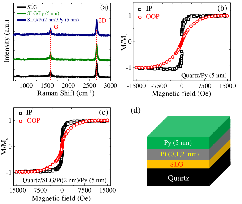
The Raman spectra of CVD-grown SLG on a Quartz before and after the deposition of Py (5 nm) and Pt(2 nm)/Py(5 nm) bilayer thin films are shown in Fig. 1a. The Raman spectra is recorded at a laser wavelength of 532 nm having a spot size of 0.5 m. The low laser power of 125 W is used to avoid any heating effect and thermal damage. The two most commonly recognised SLG signatures are the G peak at 1583.9 -1 and the 2D (or ) peak at 2677.9 -1. Here, the 2D peak is identified with second order peak of zone-boundary phonons and the G peak corresponds to a doubly degenerate zone-centre mode. We use the spectral weight ratio (2D/G) as a quantitative measure of sputtering damage. The 2D/G ratio for SLG is 2.07 ± 0.02, which remains unchanged after the deposition of Py (5 nm) and Pt(1,2 nm)/Py (5 nm) bilayer thin films Chen . The typical in-plane (open black squares) and out-of-plane (open red circles) magnetic hysteresis loops for Quartz/Py(5 nm) and Quartz/SLG/Pt(2 nm)/Py(5 nm) stack measured at room temperature are shown in Fig. 1b and Fig. 1c, respectively. The saturation magnetization (4) value was determined from the magnetic hysteresis measurement for the Quartz/Py (5 nm) sample and was found to be , while for the Quartz/SLG/Pt (2 nm)/Py (5 nm) bilayer, the value is , which agrees reasonably well with the value estimated from the FMR measurements for the same sample.
III Magnetization dynamics and spin pumping
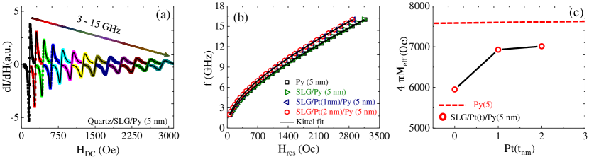
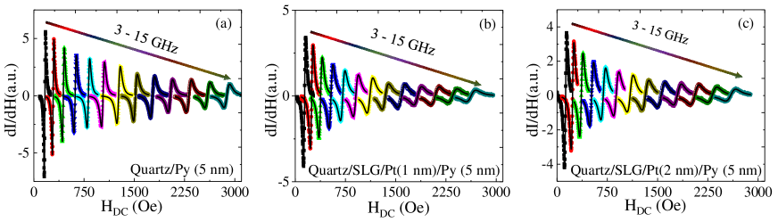
The prepared thin film stacks are subjected to the flip-chip FMR method for magnetization dynamics studies. The measurement schematic with the orientation of the relevant quantities is given in our previous reports Tahir ; Medwal . The FMR measurements are performed in static fields well above the in-plane anisotropy fields so that magnetization of the ferromagnetic layer can be considered parallel to the external magnetic field (). During magnetization precession, the ferromagnetic system absorbs the applied microwave power, thereby giving rise to the recorded FMR spectrum. The recorded FMR spectra of the Quartz/SLG/Py(5 nm) interface are shown in Fig. 2a, while the FMR spectra of the Quartz/Py(5 nm) and Quartz/SLG/Pt(1,2 nm)/Py(5 nm) interfaces are shown in Fig. 5a and Fig. 5 (b,c) in the Appendix. The derivative Lorentzian function (Eq. 3) having symmetric and asymmetric coefficients is used to fit the recorded FMR spectra Woltersdorf .
| (3) |
Here , and are the in plane applied DC magnetic field, FMR linewidth and resonance field of microwave absorption, respectively. The FMR signal’s amplitudes and correspond to symmetric and antisymmetric coefficients, respectively Woltersdorf . We evaluate the and from the fittings of the FMR spectra. The plots of microwave absorption frequency versus are shown in Fig. 2b. The effective magnetization is calculated, using Kittel’s equation (Eq. 4) Kittel .
| (4) |
Here = = GHz/T is the gyromagnetic ratio, is the Bohr magneton, is the Lande’s spectroscopic splitting factor, and is the reduced Planck’s constant, is the in-plane anisotropy field of the FM layer. The variation of as a function of the interlayer Pt thickness is shown in Fig. 2c. We find that value is higher for Quartz/Py(5 nm) sample compared to Quartz/SLG/Pt(0,1,2 nm)/Py (5 nm) samples (Fig. 2c). The value of is given by = - , where is the surface/interface anisotropy constant, is the thickness of the Py layer, and is the saturation magnetization. Since is proportional to interfacial spin-orbit coupling, we believe the decrease of for Quartz/SLG/Pt(0,1,2 nm)/Py(5 nm) is caused by the increase in interfacial spin-orbit coupling due to d-d hybridization, similar to some previous reports for 2-D/FM systems Wu ; Jamilpanah .
The surface/interface imperfections and defects in the FM thin films can enhance the linewidth of the FMR spectra. The total FMR linewidth can be expressed as:
| (5) |
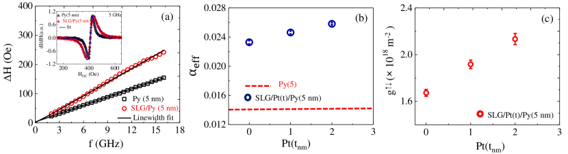
The Gilbert contributions represent the intrinsic damping. It follows from the Landau Lifshitz-Gilbert equation that the FMR linewidth would depend linearly on the microwave frequency for intrinsic damping. The variation of versus are shown in Fig. 3a. The solid line fit is given by the following equation Kittel ; Gilbert :
| (6) |
Here is the frequency-independent contribution known for inhomogeneous broadening, related to the magnetic inhomogeneity in the thin film. The linear behavior of versus confirms the intrinsic origin of the damping parameter observed in our Quartz/SLG/Py(5 nm) and Quartz/Py(5 nm) samples, as shown in Fig. 3a. The FMR spectra of Quartz/Py(5 nm) and Quartz/SLG/Py(5 nm) recorded at 5 GHz are shown in the inset of Fig. 3a. The value of = 44.58 Oe for Quartz/Py(5 nm) enhances to 52.93 Oe at 5 GHz for the Quartz/SLG/Py(5 nm) interface. Spin pumping is responsible for the enhancement in the . In the present scenario, the value of measured from the slope of the linear frequency dependence of linewidth have the following contributions:
| (7) |
Here, is the damping contribution due to energy transfer to the lattice within the bulk of the ferromagnet Hickey , whereas is mainly due to the spin pumping which is the result of the spin angular momentum loss due to spin current outflow from the FM layer into the NM layer or due to the spin-flip at the interface due to interfacial spin-orbit coupling Conca . The value of is measured as a function of inetrlayer Pt thickness as shown in Fig. 3b. A large increase in is observed for the samples Quartz/SLG/Pt(0,1,2 nm)/Py(5 nm) compared to the reference sample Quartz/Py(5 nm) as shown in Fig. 3b. The enhancement in the Gilbert damping attributed to spin-pumping is estimated by , which is utilised to calculate the interfacial spin-mixing conductance (). The interfacial spin mixing conductance () determines the amount of spin current injected or transmitted by the precessing magnetization vector of the FM layer across the interface and is given by the following expression: Tser
| (8) |
where is the saturation magnetization. The extracted values of () at the Quartz/SLG/Py(5 nm) interface is found to be increasing after the interface modification through high SOC material Pt(1,2 nm) as an interlayer. The values of () for Quartz/SLG/Py(5 nm) interface is extracted to be m-2 which is further enhanced to m-2 for Quartz/SLG/Pt/Py(5 nm) interface as shown in Fig. 3c. The enhancement of the Gilbert damping and spin mixing conductance observed in the Quartz/SLG/Pt(0,1,2 nm)/Py(5 nm) stacks could be attributed to: 1) the spin current injected in the SLG by the spin pumping mechanism at the SLG/Pt(0,1,2 nm)/Py(5 nm) interface, which creates a spin accumulation on the SLG. The dissipation of spin current at the SLG/Py and SLG/Pt/Py interfaces through spin-flip scattering acts as an additional channel for spin relaxation, leading to enhanced damping Ando1 . The diffusive flow of spins in SLG/Pt(0,1,2 nm)/Py(5 nm) can be described by spin current density , evaluated using the following expression Tser ; Tser2 :
| (9) |
Here is the RF magnetic field of Oe (at 15 dBm rf power) in the strip line of the CPW. The calculated values of are found to be dependent on interlayer (Pt) thickness and vary within the range of 0.1350.003 to 0.2420.004 MA/m2 at 3 GHz.
IV Spin current to charge current conversion
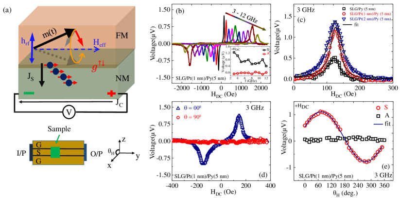
The study of spin current to charge current conversion is carried out with in-plane microwave excitation. The voltage is measured with a dc magnetic field () sweep. The measuring wires are connected to a nanovoltmeter for a direct measurement of the . In Fig. 4a, the schematic of measurement geometry of the FM/NM stack shows how spin pumping is used for the generation and flow of spin current across the FM/NM interface. A schematic of CPW shows the thin film stack in contact with the main signal transmission line (S), which is isolated from the adjacent ground line (G). In order to understand the effect of excitation frequency on the , we have performed measurements for the Quartz/SLG/Pt(0,1,2 nm)/Py(5 nm) samples in the broad frequency range of 3 to 12 GHz. Fig. 4b shows the measured vs for different values for Quartz/SLG/Pt(1 nm)/Py(5 nm) interface. The measured vs spectra are symmetric in shape and change sign with inversion of magnetic field direction which indicates that the voltage signal we measure may be primarily due to spin pumping induced spin to charge current conversion in the Pt(0,1,2 nm)/SLG interface. The sign reversal of with reversal of could be due to the fact that the where is the direction of spin polarization which gets reversed upon changing the direction of . We envisage two possibilities regarding the mechanisms responsible for spin-to-charge conversion. 1) The observed may have contributions of spin pumping induced ISHE voltage () in the Pt(1,2 nm)/SLG interface and spin-rectification effects such as anisotropic magneto resistance (AMR) and anomalous Hall effect (AHE) of the Py layer. The is supposed to generate a symmetric Lorentzian shape, while the AMR/AHE is associated with an asymmetric Lorentzian shape Ando2 ; Mosendz2 . Therefore, in order to separate the and components of voltage we have used the following Lorentzian function to fit the experimental data:
| (10) |
Best fit to the experimental data is shown by a solid black line in Fig. 4c. Inset of Fig. 4b shows the and components of voltage measured at 3 to 12 GHz frequencies for SLG/Pt(1 nm)/Py(5 nm) sample. It is clear that has significant non-zero values for all , while is close to zero throughout the frequency range. This confirms that the observed voltage signal could be due to the ISHE and certainly not AMR/AHE.
2) Spin to charge current conversion reported for 2D interfaces such as YIG/SLG Mendes , Ag/Bi JC and LAO/STO Soumyanarayanan suggests an alternative mechanism in the presence of 2D SOC driven by broken inversion symmetry. In the case of SLG/Pt(1,2 nm)/Py(5 nm) interface, we propose that initially the spin current flows into the Pt layer and diffuses with the spin diffusion length . Subsequently, it is converted into a charge current density shown in Eq. 2 by means of ISHE. This current density leads to a voltage as:
| (11) |
Here , , and are, respectively, the resistance, thickness and width of NM layer, and is a ellipticity factor and Azevedo . The reported values of spin diffusion length () and spin Hall angle () for Pt are 3.4 nm and 0.056 respectively Sanchez .
| Sample details | (A/) | ||
|---|---|---|---|
| Pt(0 nm) | 0.1350.003 | 0.0390.0002 | 0.1350.002 |
| Pt(1 nm) | 0.1590.005 | 0.1180.0005 | 0.4040.005 |
| Pt(2 nm) | 0.2420.004 | 0.1330.0003 | 0.4560.003 |
To interpret the origin of voltage in Py/SLG (Pt=0 nm) interface with the same spin pumping ISHE mechanism, we consider / , so that the expression for spin pumping voltage given by Eq. 11 reduces to:
| (12) |
The spin current is pumped from the FM layer into the Py/SLG interface and converted by the IREE into a charge current density . The measured voltage is related to this current density by . Taking into account the values of the effective thickness of SLG = m Ni , , m -2, mm and the amplitude of peak voltage V at 3 GHz for the Py/SLG interface. We observe the value of IREE coefficient nm for Py/SLG interface. The reported values of in SLG for YIG/SLG interface are of the order of nm. Mendes ; Mendes2 The spin pumping induced spin to charge current conversion voltage is enhanced for modified interfaces utilising the Pt IL, as compared to Py/SLG interface. The observed enhancement of the in Quartz/SLG/IL/Py (5 nm) interface at f = 3 GHz as shown in Fig. 4c (compared to Py/SLG) could be due to the increase of effective spin-orbit coupling due to the insertion of high SOC Pt interlayer.
To measure the voltage dependence on the out-of-plane (OOP) polar angle we rotate the sample with respect to the magnetic field. Fig. 4d shows the spectra observed at 3 GHz, with at = and for SLG/Pt(1 nm)/Py(5 nm) interface. It can be observed that the sign of at = gets reversed when is applied in the reverse direction and falls below the noise level when = as shown in Fig. 4d. Fig. 4e shows the variation of and voltage components with varying OOP angle for SLG/Pt(1 nm)/Py(5 nm) interface at 3 GHz. As already discussed, the component of voltage arises due to the AMR and AHE while the is due to the as well as AMR and AHE Lustikova . We find that is negligible and remains unchanged with variation in , while is significantly larger and varies sinusoidally with as shown in Fig. 4e. This indicates that the voltage signal measured is primarily due to the spin pumping-induced spin current-to-charge current conversion.
We calculate the value of as shown in Table 1 in order to verify the contribution of IL Pt in the spin current to charge current conversion in our SLG/Pt(0,1,2 nm)/Py interfaces. We take the value (observed for FM/SLG interface) fixed, which is of the order of . Then we calculate the value of for our SLG/Py (Pt = 0 nm) interface, which is found to be 0.1350.002 MA/m2 and 0.4040.005 MA/m2 for the SLG/Pt(1 nm)/Py interface, which further enhanced to 0.4560.003 MA/m2 for the SLG/Pt (2 nm)/Py interface. We clearly observed the enhancement in the with respect to the IL Pt thickness. Based on these findings, we speculate that the IREE may be responsible for the spin-to-charge conversion at the SLG/Py interface, while at the SLG/Pt (1,2 nm)/Py interface, both ISHE and IREE contributed to the spin-to-charge conversion.
V Conclusion
In summary, we have systematically investigated the dc voltage at the SLG/Py(5 nm) interface as a result of spin pumping induced spin current to charge current conversion by using coplanar waveguide based broadband ferromagnetic resonance setup. We have also observed the effect of the interlayer by inserting a high SOC material Pt (1,2 nm) at the SLG/Py interface. We demonstrate a strong correlation of measured spin mixing conductance and spin current to charge current conversion with the varying thickness of Pt interlayer. We contemplate that for the spin-current to charge-current conversion in our SLG/Py (5 nm) interface, the inverse Rashba-Edelstein effect is responsible, whereas in our SLG/Pt (1,2 nm)/Py (5 nm) interface, both the inverse spin Hall effect and the inverse Rashba Edelstein effect contributed to the conversion mechanism. These findings support the idea that graphene in contact with heavy metals may be a potential material for spintronic applications.
VI Acknowledgements
M.T. acknowledges the MHRD, Government of India for senior Research Fellowship. S.M. acknowledges the Department of Science and Technology (DST), Government of India for financial support. R.M. acknowledges Initiation grant, IIT Kanpur (IITK/PHY/2022027), and I-HUB Quantum Technology Foundation (I-HUB/PHY/2023288), IISER Pune for financial support.
Appendix A FMR measurements
Fig. 5 shows the recorded FMR spectra of Quartz/Py(5 nm) stack and Quartz/SLG/Pt(1,2 nm)/Py(5 nm).
Appendix B Measurement of spin current to charge current conversion in SLG/Pt(2 nm)/Py(5 nm) interface
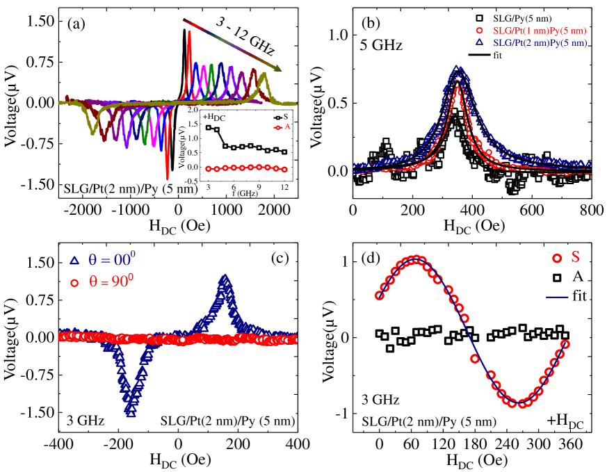
Fig. 6a shows the measured vs for different values for Quartz/SLG/Pt(2 nm)/Py(5 nm) sample. As we already discussed in the main text that the sign of gets reversed when is applied in the reverse direction. The measured vs spectra are symmetric in shape and change sign with inversion of magnetic field direction which indicates that the voltage signal we measure primarily due to spin pumping induced spin to charge current conversion in the SLG/Pt(2 nm)/Py(5 nm) interface. The spin pumping induced spin to charge current conversion voltage is enhanced for modified interfaces utilising the Pt IL, as compared to Py/SLG interface. The observed enhancement of the in Quartz/SLG/IL/Py (5 nm) interface at f = 5 GHz as shown in Fig. 6b (compared to Py/SLG) could be due to the increase of effective spin-orbit coupling due to the insertion of high SOC Pt interlayer. Best fit to the experimental data is shown by a solid black line in Fig. 6b. Inset of Fig. 6a shows the and components of voltage measured at 3 to 12 GHz frequencies for SLG/Pt(2 nm)/Py(5 nm) sample. It is clear that has significant non-zero values for all , while is close to zero throughout the frequency range. This confirms that the observed voltage signal could be due to the ISHE and certainly not AMR/AHE. To measure the voltage dependence on the OOP polar angle we rotate the sample with respect to the magnetic field. Fig. 6c shows the spectra observed at = 3 GHz, with at = and for SLG/Pt(2 nm)/Py(5 nm) interface. It can be observed that the sign of at OOP angle = gets reversed when is applied in the reverse direction and falls below the noise level when = as shown in Fig. 6c. Fig. 6d shows the variation of and voltage components with varying OOP angle for SLG/Pt(2 nm)/Py(5 nm) sample.
References
- (1) A. Fert Rev. Mod. Phys. 80, 1517 (2008).
- (2) I. Zutic, J. Fabian, and S. D. Sarma Rev. Mod. Phys. 76, 323 (2004).
- (3) S. Urazhdin, V. E. Demidov, H. Ulrichs, T. Kendziorczyk, T. Kuhn, J. Leuthold, G. Wilde and S. O. Demokritov Nature Nanotechnology 9, 509-513 (2014).
- (4) J. C. Sankey, Y.T. Cui, J. Z. Sun, J. C. Slonczewski, R. A. Buhrman and D. C. RalphNature Phys 4, 67-70 (2008).
- (5) P. F. Carcia, A. D. Meinhaldt, A. Suna Appl. Phys. Lett. 47, 178-180 (1985).
- (6) W.S. Ham, A.M. Pradipto, K. Yakushiji, K. Kim, S. H. Rhim, K. Nakamura, Y. Shiota ,S. Kim and T. Ono npj Comput Mater 7, 129 (2021).
- (7) E. Jue, C. K. Safeer, M. Drouard, A. Lopez, P. Balint, L. B.-Prejbeanu, O. Boulle, S. Auffret, A. Schuhl, A. Manchon, I. M. Miron G. Gaudin Nature Mater 15, 272-277 (2016).
- (8) X. Wang and A. Manchon Phys. Rev. Lett. 108, 117201 (2012).
- (9) A. Manchon, H.C.Koo, J. Nitta, S. M. Frolov, R. A. Duine Nat Mater.14(9), 871-82 (2015).
- (10) Y. Tserkovnyak, A. Brataas, G. E. W. Bauer, and B. I. Halperin, Rev. Mod. Phys. 77, 1375 (2005).
- (11) Y. Tserkovnyak, A. Brataas, and G. E. W. Bauer, Phys. Rev. B. 66, 224403 (2002).
- (12) Y. Tserkovnyak and A. Brataas, Phys. Rev. Lett. 88, 117601 (2002).
- (13) Y. P. Feng, L. Shen, M. Yang, A. Wang, M. Zeng, Q. Wu, S. Chintalapati and C.R. Chang WIREs Comput Mol Sci 7, e1313 (2017).
- (14) R. Urban, G. Woltersdorf, and B. Heinrich Phys. Rev. Lett. 87, 217204 (2001).
- (15) J.C.R. Sanchez, L. Vila1, G. Desfonds, S. Gambarelli, J.P. Attane, J.M. D. Teresa. C. Magen and A. Fert Nat Commun. 4, 2944 (2013).
- (16) V.M. Edelstein Solid State Commun.,73, 233-235 (1990).
- (17) E. Saitoha, M. Ueda, H. Miyajima and G. Tatara Appl. Phys. Lett. 88, 182509 (2006).
- (18) A. Azevedo, L. H. Vilela Leão, R. L. Rodriguez-Suarez, A. B. Oliveira, S. M. Rezende J. Appl. Phys.97, 10C715 (2005).
- (19) K. Shen, G. Vignale, and R. Raimondi Phys. Rev. Lett. 112, 096601 (2014).
- (20) J. Shen, Z. Feng, P. Xu, D. Hou, Y. Gao, and X. Jin Phys. Rev. Lett. 126, 197201(2021).
- (21) O. Mosendz, V. Vlaminck, J. E. Pearson, F. Y. Fradin, G. E. W. Bauer, S. D. Bader, and A. Hoffmann Phys. Rev. B 82, 214403 (2010).
- (22) J. Cheng, B.F. Miao, Z. Liu, M. Yang, K. He, Y.L. Zeng, H. Niu, X. Yang, Z.Q. Wang, X.H. Hong, S.J. Fu, L. Sun, Y. Liu, Y.Z. Wu, Z. Yuan, and H.F. Ding Phys. Rev. Lett. 129, 097203(2022).
- (23) J. E. Hirsch Phys. Rev. Lett. 83, 1834(1999).
- (24) J. Sinova, S. O. Valenzuela, J. Wunderlich, C. H. Back and T. Jungwirth Rev. Mod. Phys. 87, 1213(2015).
- (25) Z. Zhu, Y. Cheng, U. Schwingenschlögl, Phys. Rev. B 84, 153402 (2011).
- (26) K. S. Novoselov, A. K. Geim, S. V. Morozov, D. Jiang, M. I. Katsnelson, I. V. Grigorieva, S. V. Dubonos and A. A. Firsov Nature 438, 197-200 (2005).
- (27) Y. Gao, S. A. Yang, and Q. Niu Phys. Rev. Lett. 112, 166601 (2014).
- (28) A. Hoffmann and S.D.Bader Phys. Rev. Applied4, 047001 (2015).
- (29) J. Balakrishnan, G. K. W. Koon, A. Avsar, Y. Ho, J. H. Lee, M. Jaiswal, S.J. Baeck, J.H. Ahn, A. Ferreira, M. A. Cazalilla, A. H. Castro Neto and B. Özyilmaz Nat Commun5, 4748 (2014).
- (30) D. Bercioux, D. F. Urban, F. Romeo, and R. Citro Appl. Phys. Lett.101, 122405 (2012).
- (31) J.B.S. Mendes, O.A. Santos, L.M. Meireles, R.G. Lacerda, L.H.V.Leão, F.L.A. Machado, R.L. Rodríguez-Suárez, A. Azevedo, and S.M. Rezende Phys. Rev. Lett.115, 226601 (2015).
- (32) S. Singh, A. Ahmadi, C. T. Cherian, E. R. Mucciolo, E. d. Barco, B. Özyilmaz Appl. Phys. Lett. 106, 032411 (2015).
- (33) J. G. G. S. Ramos, T. C. Vasconcelos, A. L. R. Barbosa J. Appl. Phys. 123, 034304 (2018).
- (34) L.A. Benítez, J. F. Sierra, W. S. Torres, A. Arrighi, F. Bonell, M. V. Costache and S. O. Valenzuela Nature Phys 14, 303-308 (2018).
- (35) Z.Tang, E. Shikoh, H. Ago, K. Kawahara, Y. Ando, T. Shinjo, and M. Shiraishi Phys. Rev. B 87, 140401(R) (2013).
- (36) M.Tahir, D. Tiwari, A. Juyal, R. Medwal and S. Mukhopadhyay SPIN 273, 2440001 (2024) 2440001
- (37) R. Medwal, S. Gupta, R. S. Rawat, A. Subramanian, and Y. Fukuma Phys. Status Solidi RRL , 1900267 (2019).
- (38) C.T. Chen, E. A. Casu, M. Gajek, S. Raoux Appl. Phys. Lett. 103, 033109 (2013).
- (39) L. Jin, K. Jia, D. Zhang, B. Liu, H. Meng, X. Tang, Z. Zhong, and H.Zhang ACS Appl. Mater. Interfaces. 11, 35458 (2019).
- (40) G. Woltersdorf, Ph.D. dissertation Simon Fraser University (2004).
- (41) G.Wu, Y.Ren, X.He, Y.Zhang, H.i.Xue, Z.Ji, Q.Y.Jin, and Z. Zhang PHYSICAL REVIEW APPLIED 13, 024027 (2020).
- (42) L.Jamilpanah, M.Hajiali, S.M. Mohseni Journal of Magnetism and Magnetic Materials 514, 1672 (2020).
- (43) C. Kittel, Phys.Rev. 73, 155 (1948).
- (44) T. L. Gilbert IEEE Transactions on Magnetics 40, 3443-3449 (2004).
- (45) M. C. Hickey and J. S. Moodera Phys. Rev. Lett. 102, 137601 (2009).
- (46) A. Conca, S. Keller, L. Mihalceanu, T. Kehagias, G. P. Dimitrakopulos, B. Hillebrands, and E. T. Papaioannou, Phys. Rev. B. 93, 134405 (2016).
- (47) K. Ando, S. Takahashi, J. Ieda, Y. Kajiwara, H. Nakayama, T. Yoshino, K. Harii, Y. Fujikawa, M. Matsuo, S. Maekawa, E. Saitoh J. Appl. Phys. 109, 103913 (2011).
- (48) K. Ando and E. Saitoh, Nat. Commun. 3, 629 (2012).
- (49) O. Mosendz, J. E. Pearson, F. Y. Fradin, G. E. W. Bauer, S. D. Bader, and A. Hoffmann, Phys. Rev. Lett. 104, 046601 (2010).
- (50) A. Soumyanarayanan, N. Reyren, A. Fert, and C. Panagopoulos, Nature (London) 539, 509 (2016).
- (51) A. Azevedo, L. H. Vilela Leao, R. L. Rodriguez Suarez, A. F. Lacerda Santos, and S. M. Rezende Phys. Rev. B 83, 144402 (2011).
- (52) A. Azevedo, L. H. Vilela Leao, R. L. Rodriguez Suarez, A. F. Lacerda Santos, and S. M. Rezende Phys. Rev. B 83, 144402 (2011).
- (53) J.C.R.Sanchez, N. Reyren, P.Laczkowski, W. Savero, J.P.Attane, C.Deranlot, M.Jamet, J.M. George, L. Vila, and H.Jaffres Phys. Rev. Lett. 112, 106602 (2014).
- (54) Z. H. Ni, H. M. Wang, J. Kasim, H. M. Fan, T. Yu, Y. H. Wu, Y. P. Feng, and Z.X. Shen. Nano Lett. 7, 9, 2758-2763 (2007).
- (55) J. B. S. Mendes, O. A. Santos, T. Chagas, R. M. Paniago, T. J. A. Mori, J. Holanda, L. M. Meireles, R.G.Lacerda, A. Azevedo, and S. M. Rezende Phys. Rev. B 99, 214446 (2019).
- (56) J. Lustikova, Y. Shiomi, and E. Saitoh Phys. Rev. B 92, 224436 (2015).