Fabrication of planar halfmetallic ferromagnetic Josephson junctions with long range coupling
Abstract
Superconducting junctions with a ferromagnet as the weak link, where triplet correlations can transport supercurrents over a substantial distance, have been of long-standing interest. In this work, we study the triplet transport in planar La0.7Sr0.3MnO3(LSMO) nanowire Josephson junctions with NbTi superconducting contacts. By meticulous ion etching with an artificial Pt hard mask, the NbTi/LSMO bilayer is structured to form an LSMO bridge without damaging its top layer. We observe superconducting (critical) currents of the order of 109 A/m2 in a junction with a length of 1.3 m, and distinguishing superconducting quantum interference (SQI) patterns when sweeping a magnetic field perpendicular () to the plane of the wire or parallel () to the plane and along the wire. The observed Gaussian-shaped SQI pattern is attributed to the diffusive transport of triplet pairs in the LSMO. Our work demonstrates that combinations of oxide magnets with conventional (-wave) alloy superconductors can be a promising new route to realizing superconducting spintronics.
In Josephson junctions of two superconductors (S) with a halfmetallic ferromagnetic (HMF) weak link, it is possible to convert conventional (spinless) Cooper pairs to equal-spin triplets that can in principle carry supercurrents over micrometer distances. This long range proximity (LRP) effect stems from the fully spin-polarized nature of the HFM, in which the triplets are not susceptible to pairbreaking exchange fields. The singlet-triplet conversion requires some form of spin mixing at the S/HMF interface, which can be in the form of magnetic inhomogeneities, or engineered by inserting additional ferromagnetic (F) layers. Long range effects have been reported in various experiments on devices with planar geometries [1, 2, 3, 4]. Triplets were generated in CrO2-based hybrids via magnetic inhomogeneities established either by strain or disorder of grain boundaries [5], while high-density critical supercurrents were observed using stacked S/F/CrO2 geometries [3]. Similarly, the LRP effect was studied in combinations of the high-Tc superconductor YBa2Cu3O7(YBCO) and the magnetic manganites La0.7Ca0.3MnO3(LCMO) and La0.7Sr0.3MnO3(LSMO) [4, 6]. Visani et al. reported equal-spin Andreev reflections at the interface between YBCO and LCMO in a vertical architecture, as well as the existence of triplets in the LCMO layer of 30 nm [6]. Interestingly, uncompensated magnetic moments were discovered at the Cu-O-Mn chains across the interface between YBCO and LCMO that could be a source of magnetic inhomogeneity, although the relation to triplet generation was not elucidated [7]. Very recently, extremely long coherent transport of triplets was found in lateral YBCO/LSMO/YBCO junctions [4]. Sanchez-Manzano et al. observed LRP effects in quite wide (20 or 25 m) but also quite long (1 m) LSMO wires, where multiple magnetic domain walls were present and possibly played a role in triplet generation and transport. Despite the LRP effect being unequivocally observed in the high-Tc S/HMF systems, the underlying physics, in particular with respect to the triplet generation, still remains to be explored.
To further study the triplets generation and transport in HMF, in this work we fabricated lateral junctions of LSMO with the conventional superconductor NbTi, by carefully ion etching grown NbTi/LSMO bilayer using artificial Pt hard masks. By starting from a bilayer, we avoided contamination of the LSMO/NbTi interface as it would occur when transfering the LSMO film - for further processing. NbTi does not grow epitaxially on LSMO, differing from the high- S/HMF systems, but we know from earlier work that triplets are generated at the NbTi/LSMO interface [8]. The removal of the NbTi on LSMO was examined by energy-dispersive X-ray spectroscopy (EDS) characterizations and electrical resistance measurements, confirming the LSMO-based junctions. We observed the LRP effect in a junction with 1.3 m length and 5 m width. The critical current of this junction reached 11108 A/m2 at 1.5 K. By sweeping the magnetic fields (perpendicular to the plane of the wire) and (field in-plane and along the wire) at 6.3 K, just below the temperature where zero resistance is reached, distinguishing superconducting quantum interference (SQI) patterns were obtained. We attribute those Gaussian-shaped SQI patterns to the diffusive transport of triplets in LSMO. Our work demonstrates that strong triplet supercurrent can be found in conventional (-wave) alloy S/HMF junctions. This may shed light on understanding the generation and transport of triplets in HMFs, and also offers a platform for spintronics-type applications.
| Step IV | Step VI | ||||
| thickness(nm) | etch rate(nm/min) | etch time(min) | thickness (nm) | etch time(min) | |
|---|---|---|---|---|---|
| Pt | 9 | ||||
| NbTi | 9 | ||||
| LSMO | |||||
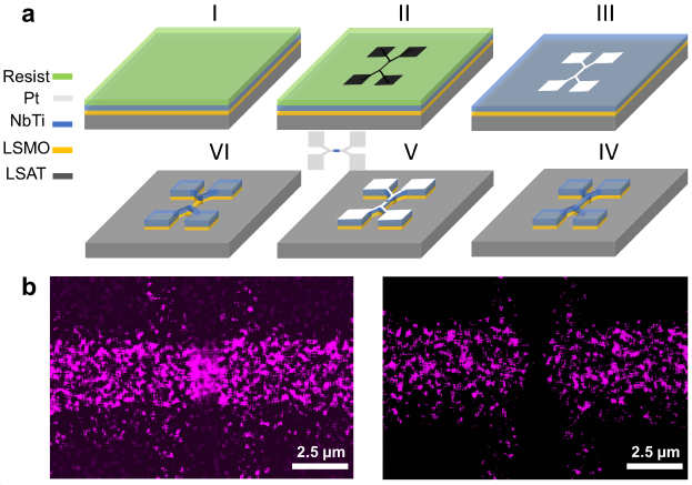
We fabricated the lateral NbTi/LSMO junctions by carefully and accurately etching the NbTi/LSMO bilayer with an artificial Pt hard mask. By starting from a bilayer, the interface between NbTi and LSMO is not damaged. The details of the nanofabrication process are schematically depicted step by step in Fig. 1a.
The starting point for the fabrication is growing a NbTi/LSMO bilayer. The LSMO thin film (40 nm) was deposited on a (001)-oriented LSAT crystal substrate at 700 in an off-axis sputtering system. The deposition pressure was kept at 0.7 mbar by flowing a mix of Argon and Oxygen gas (3:2). The sputtering power was 50 W. Still at the deposition pressure, the system was cooled down to room temperature. At first, the cooling rate is 25 /min, but we waited several hours to reach a low temperature and minimize possible issues with interdiffusion. The epitaxy of the LSMO film was confirmed before [8]. Then the system was pumped down to 10-7 mbar, followed by the sputter deposition of NbTi (60 nm) on the LSMO layer , in an Ar atmosphere with a pressure of 0.1 mbar.
Next, a positive e-beam resist was spin-coated on the NbTi/LSMO bilayer, and a pattern was written by exposure to an electron beam (Fig. 1a-I, II). The etch rate of resist is high in ion beam etching (IBE), and the resist mask will be removed completely before succeeding to pattern the NbTi/LSMO bilayer. Therefore, the sample with the patterned resist layers was loaded into an on-axis radio-frequency sputtering system, and a thick Pt layer (426 nm) was deposited. After lifting off, the Pt served as a hard mask protecting the NbTi/LSMO bilayer (Fig. 1a-III). In the next step, shown in Fig. 1a-IV, the NbTi/LSMO bilayer was patterned. In this step, the Pt layer is (almost) fully removed, but the bilayer should be intact. To open up a gap and form a junction, i.e. making LSMO the weak link, the NbTi needs to be removed. For this, we repeated the above procedure with Pt liftoff. The difference in this step was that the central part of the nanowire was uncovered by the Pt hard mask and hence the IBE removed the NbTi in that part (Fig. 1a-V). Crucial here is that the thickness of the Pt layer is chosen such that it is removed during the same etch time that removes the 60 nm NbTi layer. In this way, we obtained well-defined lateral NbTi/LSMO/NbTi junctions with adjustable widths and lengths (Fig. 1a-VI).
As mentioned, several etch steps in the procedure depend crucially on the etch rate for the different materials. These were collected in a series of precise measurements on films of the relevant materials, involving thickness measurements by small-angle x-ray diffraction and Atomic Force Microscopy. Here we summarize details of the etch process and give the etching rates that we found and used in step IV (removing the Pt mask from the full structure), and step VI (removing the NbTi on top of the LSMO bridge). Thicknesses, etch rates, and etch times are given in Table 1.
Subsequent to the nanofabrication, we employed energy-dispersive X-ray spectroscopy (EDS) to qualitatively examine the NbTi/LSMO junctions. We mapped the element Nb, as shown in Fig. 1b. Before etching, a relatively strong EDS signal was observed Nb (left image in Fig. 1b), which was absent after optimal etching (right image in Fig. 1b). Given the resolution of a few nm, this does not prove we fully removed the Nb, but it shows that we did etch Nb in the intended area. In all, we fabricated four measurable devices in this way, two with bridge widths around 2 m (called DV2 and DV3), and three with bridge widths of about 5 m (called DV4, DV5, DV6). Device DV2 had a too low Tc to be measured, DV5 was used for etch tests, and DV6 could only be measured at one temperature because of a cryostat problem. Both DV3 and DV4 showed the desired LRP effects. Below, we discuss the data on DV4 and DV5 as the purpose of the paper is to establish proof-of-principle regarding the device fabrication.
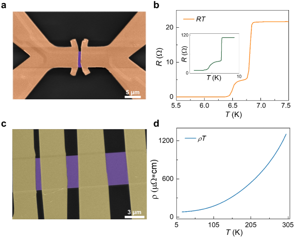
The electrical transport measurements also lead to the conclusion that the etching has removed the NbTi layer, and that an LSMO-based junction is formed. First we measured the temperature-dependent resistance (-) of junction DV5, using a current of 1 A (as in all - measurements). The length of the junction and the width of the central bridge are determined to be 0.766 m and 4.89 m, respectively, by scanning electron microscopy (SEM) (Fig. 2a). The - data after the etching are shown in Fig. 2b (orange curve). We observe the well-known signature of a proximized structure, where the banks become superconducting first, followed by a plateau that is determined by the resistance of the weak link, and then a resistance drop to zero when the link becomes fully superconducting. The first drop is seen around 6.9 K, the second one below 6.5 K. The relatively low Tc of the NbTi is due to a background pressure of 10-7 mbar and the fact that NbTi is a good getter.
We can approximately calculate the (expected) resistance of the junction in case the weak link consists of LSMO. The resistivity of a typical LSMO nanowire with a width of 5 m was measured using the four-probe method, as shown in Fig. 2c. The is determined to be 80 cm at 10 K (Fig. 2d). According to , is the length, and is the cross-section area, we obtain . The measured resistance of the junction is about 5 , slightly larger than the calculated value, indicating the LSMO layer is a bit over-etched. Further etching leads to an 8 times increase in the resistance (inset in Fig. 2b) since now also the NbTi of the contacts is being etched. Since IBE is utilized to remove the unwanted NbTi layer, it may also contaminate the LSMO layer if the etching time is not optimized, leading to a pronounced increase in resistance. Therefore, we take the optimal etching to make the NbTi/LSMO junctions to ensure the NbTi is completely removed, and LSMO is slightly etched to form a ferromagnetic weak link.
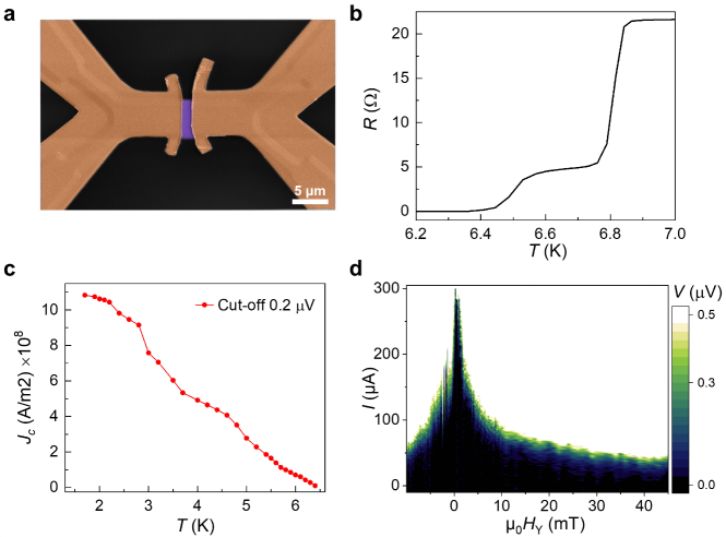
Having fabricated the lateral NbTi/LSMO junctions, we performed transport measurements on junction DV4 with 1.3 m length () and 5 m width () (Fig. 3a), by changing temperature and sweeping fields, yielding and SQI characterizations. The curve was plotted in Fig. 3b. The resistance of the junction decreases to zero after two transitions. The first transition corresponds to the superconducting NbTi, leaving a residual resistance of 6 . We take 80 cm, 5.2 , meaning LSMO is over-etched optimally in this junction. The second transition signifies the onset of the superconductivity in the weak link, indicating LSMO is fully proximized. The LRP effect over such a long length is not inconceivable. Sanchez-Manzano et al. reported the LRP effect in very wide YBCO/LSMO junctions (20 and 25 m), with a length of about 1 m, although with much lower critical currents [4]. Therefore, we thoroughly inspected the observed superconductivity in the junction here. The behavior of the critical current density () versus temperature was measured first and summarised in Fig. 3c by taking a criterion of 0.2 V. At the base temperature (1.5 K), is about 11108 A/m2, which is a really high value over such as long length.
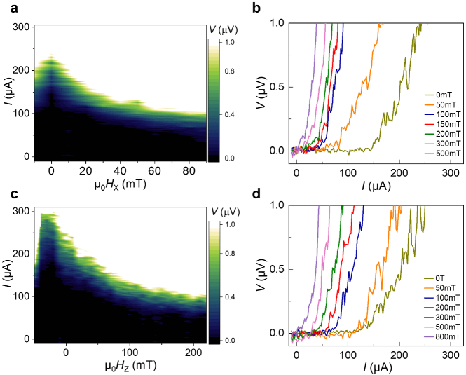
To further confirm the Josephson coupling, we examined the SQI pattern of the junction by applying a magnetic field ( direction; perpendicular to the sample plane) at 6.3 K (Fig. 3d). The obtained SQI pattern is far from the typical Fraunhofer-like pattern. Instead, it is quasi-Gaussian-like with a rather sharp decay of . If we ignore the shielding currents in the side NbTi arms, the first minimum for the Fraunhofer pattern would be expected at . This yields 0.3 mT. Therefore, the expected period is very small (actually smaller than can be easily measured), but the observed pattern is wider and falls off more slowly. Note that, from the measured resistivity of LSMO (40 cm), its mean free path () is about 6.5 nm [9]. With a Fermi velocity of m/s and using = 6.4 K, we find the diffusive coherence length to be 17.5 nm. Given the length of the junction of about 1.3 m, the case we deal with, for the triplet transport, is that of a diffusive long junction (). That can lead to a Gaussian-shaped curve of the form under the condition that [10, 11, 12]. Here is the total flux threading the junction, is a geometry-dependent constant, and is the flux quantum. The problem is that for this junction, , which should lead to a Fraunhofer pattern. Here we have to remember that we are dealing with a magnetic structure with internal magnetic fields. The phase accumulation along paths, i.e. along the width or along the length of the wire may well be different. A more quantitative description has not been made yet [13, 14, 15].
Afterward, we recorded the SQI patterns with (field in plane along the wire) at 6.3 K, as shown in Fig. 4. With along the long axis ( direction) or short axis ( direction) of the wire, the obtained SQI patterns behave quite differently. The central peaks are much wider than that of the SQI pattern with . Fig. 4a,c show the critical current decays far more gradually. The curves measured at different fields demonstrate vanishes at the fields of the order of hundreds of mT (Fig. 4b and d). The curves become nearly linear at 500 mT (along ) and 800 mT (along ). Note that the direction is the current direction, and in the configuration B , no SQI is to be expected.
To summarize, we developed a nanofabrication method to fabricate long lateral NbTi/LSMO Josephson junctions. The process starts with bilayer films and involves using a hard mask of Pt, and a series of lithography steps. One crucial step is the removal of the 60 nm NbTi layer on the LSMO bridge. By slightly overetching, the EDS and resistance measurements confirm that LSMO-based junctions have been made, with absence of NbTi shorts. We measured and characterized a junction with 1.3 m length and 5 m width by measuring the temperature dependence of and recording the SQI patterns with either or . The junction has a critical current of 11 108 A/m2 at 1.5 K. Distinguishing Gaussian-shaped SQI patterns are observed with the fields along different directions. We fabricated several devices that showed a full proximity effect in their characteristics. What still needs to be improved is understanding of, and control over, the triplet generator. As to control, a device (DV3) with a smaller bridge width (2 m), and a smaller length (0.59 m) showed a smaller value of at 1.5 K (5 108 A/m2) than the longer device mentioned above. This length dependence is the focus of current experiments, the more so since the results for DV4 hint at the possibility of still longer lengths. With respect to understanding, similar to the YBCO/LSMO case, we did not build in an extra magnetic layer to enhance spin scattering. Preliminary transmission electron microscopy data indicate that the oxygen concentration at our NbTi/LSMO interface is anomalous, which might give rise to inhomogeneous magnetism [16]. We surmise that these long junctions will open the way to further producing spin torque effects and manipulating local spins or even moving domain walls without Joule heating, giving rise to actual applications in superconducting spintronics.
Acknowledgments
The authors thank Kaveh Lahabi and Remko Fermin for discussions, and Marcel Hesselberth and Douwe Scholma for support in device preparation. Y.J. was partially funded by China Scholarship Council (Grant No. 201808440424). The work is partly financed by the Dutch Research Council (NWO) through Projectruimte Grant No. 680.91.128 and Project OCENW.XS22.2.032. The work was further supported by EU Cost Action CA21144 (SUPERQUMAP).
Author Declarations
Conflicts of interest
The authors declare no competing interests
Author contributions
Yunxiang Yao: Conceptualization (equal); Data curation (lead); Formal analysis (lead); Funding acquisition (supporting); Investigation (lead); Methodology (equal); Project administration (support); Resources (lead); Software (lead); Supervision (supporting); Validation (equal); Visualization (lead); Writing – original draft (lead); Writing – review & editing (equal). Jan Aarts: Conceptualization (equal); Data curation (supporting); Formal analysis (supporting); Funding acquisition (lead); Investigation (supporting); Methodology (equal); Project administration (lead); Resources (supporting); Software (supporting); Supervision (lead); Validation (equal); Visualization (supporting); Writing – original draft (supporting); Writing – review & editing (equal).
Data availability
The data that support the findings of this study are available from the corresponding authors upon reasonable request.
References
- Keizer et al. [2006] Ruurd S Keizer, Sebastian TB Gönnenwein, Teun M Klapwijk, Guoxing Miao, Gang Xiao, and Arunava Gupta. A spin triplet supercurrent through the half-metallic ferromagnet CrO2. Nature, 439(7078):825–827, 2006.
- Anwar et al. [2010] MS Anwar, F Czeschka, M Hesselberth, M Porcu, and J Aarts. Long-range supercurrents through half-metallic ferromagnetic CrO2. Physical Review B, 82(10):100501, 2010.
- Singh et al. [2016] Amrita Singh, Charlotte Jansen, Kaveh Lahabi, and Jan Aarts. High-quality cro 2 nanowires for dissipation-less spintronics. Physical Review X, 6(4):041012, 2016.
- Sanchez-Manzano et al. [2022] D Sanchez-Manzano, S Mesoraca, FA Cuellar, M Cabero, V Rouco, G Orfila, X Palermo, A Balan, L Marcano, A Sander, et al. Extremely long-range, high-temperature josephson coupling across a half-metallic ferromagnet. Nature Materials, 21(2):188–194, 2022.
- Anwar and Aarts [2011] MS Anwar and J Aarts. Inducing supercurrents in thin films of ferromagnetic cro2. Superconductor Science and Technology, 24(2):024016, 2011.
- Visani et al. [2012] C Visani, Z Sefrioui, J Tornos, C Leon, J Briatico, M Bibes, A Barthélémy, J Santamaria, and Javier E Villegas. Equal-spin andreev reflection and long-range coherent transport in high-temperature superconductor/half-metallic ferromagnet junctions. Nature Physics, 8(7):539–543, 2012.
- Chakhalian et al. [2006] Jak Chakhalian, JW Freeland, G Srajer, J Strempfer, G Khaliullin, JC Cezar, T Charlton, R Dalgliesh, Ch Bernhard, G Cristiani, et al. Magnetism at the interface between ferromagnetic and superconducting oxides. Nature Physics, 2(4):244–248, 2006.
- Jungxiang et al. [2023] Yao Jungxiang, Remko Fermin, Kaveh Lahabi, and Jan Aarts. Triplet supercurrents in lateral josephson junctions with a half-metallic ferromagnet, 2023. URL https://arxiv.org/abs/2303.13922.
- Nadgorny et al. [2001] B. Nadgorny, II. Mazin, M. Osofsky, RJ Soulen, P. Broussard, RM Stroud, DJ. Singh, V.G. Harris, A. Arsenov, and Y. Mukovskii. Origin of high transport spin polarization in La0.7Sr0.3MnO3: Direct evidence for minority spin states. Physical Review B, 63:184433, 2001.
- Cuevas and Bergeret [2007] J. C. Cuevas and F. S. Bergeret. Magnetic interference patterns and vortices in diffusive sns junctions. Physical Review Letters, 99:217002, 2007.
- Chiodi et al. [2012] F Chiodi, M Ferrier, S Guéron, JC Cuevas, G Montambaux, F Fortuna, A Kasumov, and H Bouchiat. Geometry-related magnetic interference patterns in long s n s josephson junctions. Physical Review B, 86(6):064510, 2012.
- Barone and Paterno [1982] Antonio Barone and Gianfranco Paterno. Physics and applications of the Josephson effect, volume 1. Wiley Online Library, 1982.
- Suominen et al. [2017] HJ Suominen, J Danon, M Kjaergaard, K Flensberg, J Shabani, CJ Palmstrøm, F Nichele, and CM Marcus. Anomalous fraunhofer interference in epitaxial superconductor-semiconductor josephson junctions. Physical Review B, 95(3):035307, 2017.
- Börcsök et al. [2019] Bence Börcsök, Sachio Komori, AI Buzdin, and JWA Robinson. Fraunhofer patterns in magnetic josephson junctions with non-uniform magnetic susceptibility. Scientific Reports, 9(1):1–6, 2019.
- Alidoust et al. [2018] Mohammad Alidoust, Morten Willatzen, and Antti-Pekka Jauho. Fraunhofer response and supercurrent spin switching in black phosphorus with strain and disorder. Physical Review B, 98(18):184505, 2018.
- [16] M. Cabero Piris, private communication.