Nanoscale single-electron box with a floating lead for quantum sensing: modelling and device characterization
Abstract
We present an in-depth analysis of a single-electron box (SEB) biased through a floating node technique that is common in charge-coupled devices (CCDs). The device is analyzed and characterized in the context of single-electron charge-sensing techniques for integrated silicon quantum dots (QD). The unique aspect of our SEB design is the incorporation of a metallic floating node, strategically employed for sensing and precise injection of electrons into an electrostatically formed QD. To analyse the SEB, we propose an extended multi-orbital Anderson impurity model (MOAIM), adapted to our nanoscale SEB system, that is used to predict theoretically the behaviour of the SEB in the context of a charge-sensing application. The validation of the model and the sensing technique has been carried out on a QD fabricated in a fully depleted silicon-on-insulator (FD-SOI) process on a 22-nm CMOS technology node. We demonstrate the MOAIM’s efficacy in predicting the observed electronic behavior and elucidating the complex electron dynamics and correlations in the SEB. The results of our study reinforce the versatility and precision of the model in the realm of nanoelectronics and highlight the practical utility of the metallic floating node as a mechanism for charge injection and detection in integrated QDs. Finally, we identify the limitations of our model in capturing higher-order effects observed in our measurements and propose future outlook to reconcile some of these discrepancies.
Single-electron boxes (SEB) are a type of nanoscale electronic devices comprising a quantum dot (QD) coupled to a metallic lead through a tunneling junction Nazarov and Blanter (2009). The chemical potential of the QD is controlled by a gate, coupled capacitively to it (implying no current flowing from the gate to the QD). The distinctive properties of single-electron boxes emerge as a consequence of their nanoscale dimensions, where the quantum nature of charge carriers becomes pronounced, giving rise to phenomena such as Coulomb blockade and quantum tunneling, especially at low temperatures Yadav et al. (2022); Goodnick and Bird (2003).
Quantum properties of SEBs make them extremely charge-sensitive, and these devices can be fabricated with precision engineering. In the light of the immense progress in semiconductor qubit technologies Anders et al. (2023), there is an increasing interest in sensitive electrometers for silicon spin qubits that would take up a small area and be compatible with large-scale integration. SEB electrometers have been proposed to be used as charge sensors for qubits Bashir et al. (2020); Filmer et al. (2020); Power et al. (2022); Oakes et al. (2023); Mihailescu et al. (2023) or even as quantum thermometers Mihailescu, Campbell, and Mitchell (2023). For that reason, probing the state of a SEB device made on a commercial process will be of particularly great benefit for developing quantum sensing applications.
In this paper, we present a SEB which is formed by a metallic node (lead) coupled to an electrostatically formed semiconductor QD. The key feature of this study is that the biasing and detecting of the SEB charge states is carried out through a scheme that is inspired by a technique common to the output stage of charge-coupled devices (CCDs) Janesick et al. (1990). It is worth noting that CCDs might also be addressing the problem of single-electron detection but in the context of digital imaging Abramoff et al. (2019); Tiffenberg et al. (2017). Being essentially large-scale integrated systems, CCDs are particularly compatible with commercial and non-commercial semiconductor processes, and the measurement in CCDs are carried out in the charge domain. The feasibility of such biasing schemes has been demonstrated in Ref. Bashir et al. (2020). Moreover, quantum nanoelectronics devices lithographically defined in semi-conducting 2D electron gas (2DEG) structures have been integrated recently with charge sensors to measure entropy changes in QD devices Child et al. (2022); Han et al. (2022).
The device is implemented in a commercial fully depleted silicon-on-insulator process on a 22-nm CMOS technology node by GlobalFoundries. Since the QD of the SEB is controlled electrostatically, we are interested in deriving its quantum mechanical model taking into account effective orbitals and potential shape formation fluctuations and asymmetries which are the aspects of realistic QDs. For this reason, we develop a type of multi-orbital Anderson impurity model Hewson (1993) (MOAIM) to predict the observed voltage from the SEB under the CCD biasing and measurement scheme. We then compare the SEB experimental characterization at a temperature of 3.5 K with the model and show that the SEB responds to individual charge transitions. This illustrates that it is possible to utilize SEB-CCD electrometers in integrated semiconductor QDs.
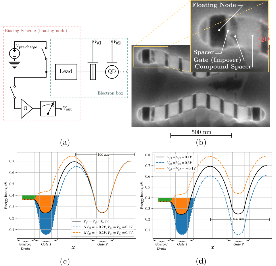
The system is presented in Fig. 1. The scheme of the SEB and its biasing principle are illustrated in Fig. 1(a). The SEB consists of an electrostatically defined semiconductor QD whose chemical potential is controlled by the gate voltage . There is a (metal) lead whose Fermi energy is lying above the edge of its conduction band. The lead is connected to the QD through a tunneling junction. The Fermi energy of the lead is controlled by the biasing circuit in the following way. A switch is activated to connect the lead to a voltage source that elevates the potential of the lead to some . The switch is deactivated after this, and the node is disconnected from the voltage source — it is in a “floating” state where any change in the number of electrons will result in a significant change of its electric potential due to its small capacitance. Next, the voltage at the gate terminal is adjusted to tune the alignment of the Fermi energy of the lead to the chemical potential of the dot, allowing the tunneling of an electron from the lead to the QD. The second switch is then activated to measure if the electric potential of the lead has changed compared to the original state due to an electron tunneling to the QD. The capacitance of the lead is estimated (via parasitic extraction) to be fF. The target design gain of the voltage amplifier is (the gain is subject to process variability). This results in an expected 16 mV step at the output of the voltage amplifier per one electron removed from the lead to the QD. The temperature of the set-up is K.
The SEM image of the lead and the QD is shown in Fig. 1(b). While it is a part of a large QD array, we apply low voltages at all the gates. This results in a very large potential energy barrier separating the quantum dots from each other. We then can control the tunnelling junction between the reservoir of electrons (lead) and the first quantum dot, while keeping the other dots isolated. The parameters of the devices are given in the figure caption.
The top view of the system is shown in Fig. 1(b). The thin Si-film results in a transversal confinement causing a 2DEG behavior of electrons in the film and the in-plane confinement is controlled by the gates. In this class of devices, the formation of wells of the conduction band is defined electrostatically. The dot can form either below the gates or in the spaces between the gates depending on and other controlled voltages (such as the common-mode voltage ). In the test presented in this paper, at mV (after the pre-charge stage, the lead acquires a negative potential) and ranging up to V, a shallow well is formed below the gates (except for the very first one, adjacent to the lead that forms an extended electron reservoir due to diffusion on electrons). The self-consistent simulation of the conduction band and charge carrier density at 3.5 K, presented in Fig. 1(c) and (d), confirms this assumption. (A single-gate test device was also tested by the means of transport measurement to confirm this.) In this study, we present the results of two different samples that have some variations in the shape of the lead, the spacer and the gate.
In order to perform QD injection, spectroscopy and characterization of its underlying physics, we firstly need to build a theoretical quantum model that can describe and predict the system’s behavior. For the purpose of capturing the physical interactions and factors that contribute to the many-body dynamics of the QD, we employ an extended Fermi-Hubbard model for effective quantum orbitals. The quantum model that describes the QD is expressed by the following Hamiltonian:
where is the on-site potential for orbital , is the electrostatic Coulomb coupling between an electron at orbital and spin and another electron at orbital and spin with ,
is the Fock space fermionic annihilation (creation) operator for a fermion at orbital and spin and is the number operator.
The creation/annihilation operators satisfy the fermionic algebra anti-commutation relations and and act upon the system’s Fock space; for fermions it is defined as , with being the fermion Hilbert subspace.
For the physical specifications of our system we have taken the QD to be of volume nm3 and to be composed of effective orbitals for sample A and for sample B; these are chosen phenomenologically and ad-hoc. The dimensions of the dot are taken from the physical parameters of the system, and will provide a very good correspondance to the observed energy levels. Since nm and so , we restrict ourselves to the orbitals formed due to confinement in the smaller dimensions. The contributing energies are the Coulomb intra and inter-orbital coupling energies meV (Si), and the effective on-site confinement energies (meV) and (meV), with for . These are derived from a symmetric finite quantum well calculation, fine-tuned by a common-mode voltage mV (which is close to the mV used in QTCAD) and since our formed QD need not be completely symmetrical, we add a random fluctuation of the energy levels to account for potential imperfections in our electrostatically formed QD. That is, we have , with sampled from a normal distribution with mean and standard deviation . Finally we utilize the transversal and longitudinal electron masses Kittel (2004) as (Si) and (Si), respectively.
| Number of electrons | Fock space eigenstate |
|---|---|
| ⋮ | ⋮ |
In addition to the above Hamiltonian which describes the dynamics of the isolated QD, we employ a lead Hamiltonian , which corresponds to the metallic floating node in the actual structure. We treat it as a semi-classical reservoir of electrons, from which they can jump in and out, with different energies and a Fermi level controlled externally through manipulation of a tunable electrochemical potential . We include only a left lead () coupled to the QD. In addition, we add the coupling between the lead and the QD (hybridization), so the total Hamiltonian for our SEB will have the form of a MOAIM:
| (1) |
with with the energy of the level and spin of the metallic node Hamiltonian, the fermionic annihilation (creation) operator of an electron of energy level and spin in the lead, the hybridization (coupling) energy between each lead level and the QD and is the Hermitian conjugate counterterm.
We consider a uniform hybridization which is also manipulated via gate voltages in the device. In our simulation, its values range in the = 3–40 eV regime, which satisfies for any energy scale of our system. The full Hamiltonian can then be used to model the quantum transport properties of the system, and how the QD electronic occupation depends on applied potentials Kouwenhoven et al. (1997); Shangguan et al. (2001); Gurvitz (1998).
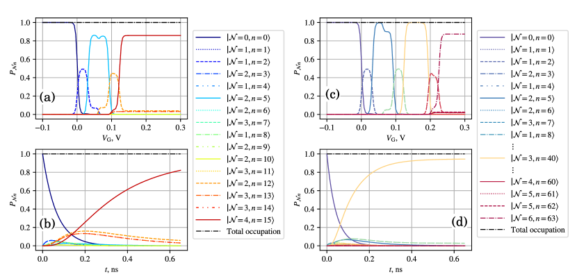
We treat the QD in Fock space, allowing up to and electrons to occupy the structure for sample A and sample B, respectively. Our density matrix , with , the Hubbard operator has diagonal elements , with , and we show them symbolically in Table 1. Each of the Fock eigenstates with electrons will be a superposition of states, with .
We assume that the lead is weakly coupled to the QD and therefore keep up to second-order hybridization terms , so we can ignore off-diagonal elements in and significant mixing of Fock space states. Consequently, the dynamical evolution of the population numbers is simplified to a set of partial differential master equations Fransson and Råsander (2006):
| (2) |
| (3) |
| (4) |
where is the tunneling rate between the metallic lead and the QD with is the energy difference between the two Fock eigenstates, are the transition elements, is the Dirac delta function, is the Fermi-Dirac statistical function and .
Initializing our system with no electrons in it, , we show the dependence of the population numbers close to equilibrium (steady state), with respect to of the lead in Fig. 2(a) for sample A and Fig. 2(c) for sample B, respectively. We can see the dynamic evolution of the Fock states to approach thermal equilibrium in Fig. 2(b) for sample A and in Fig. 2(d) for sample B. Given some initial conditions, there is a clear threshold electrochemical lead potential (i.e. gate voltage ) for which we have a many-body stochastic injection in the structure which is related to the energy level spacing between the lead and the first non-trivial Fock state of the QD. Using the population numbers and the corresponding electron number of each Fock state, we can compute an average:
| (5) |
where and is the number of electrons and occupational number of state in the QD for an electrochemical potential and temperature , respectively.
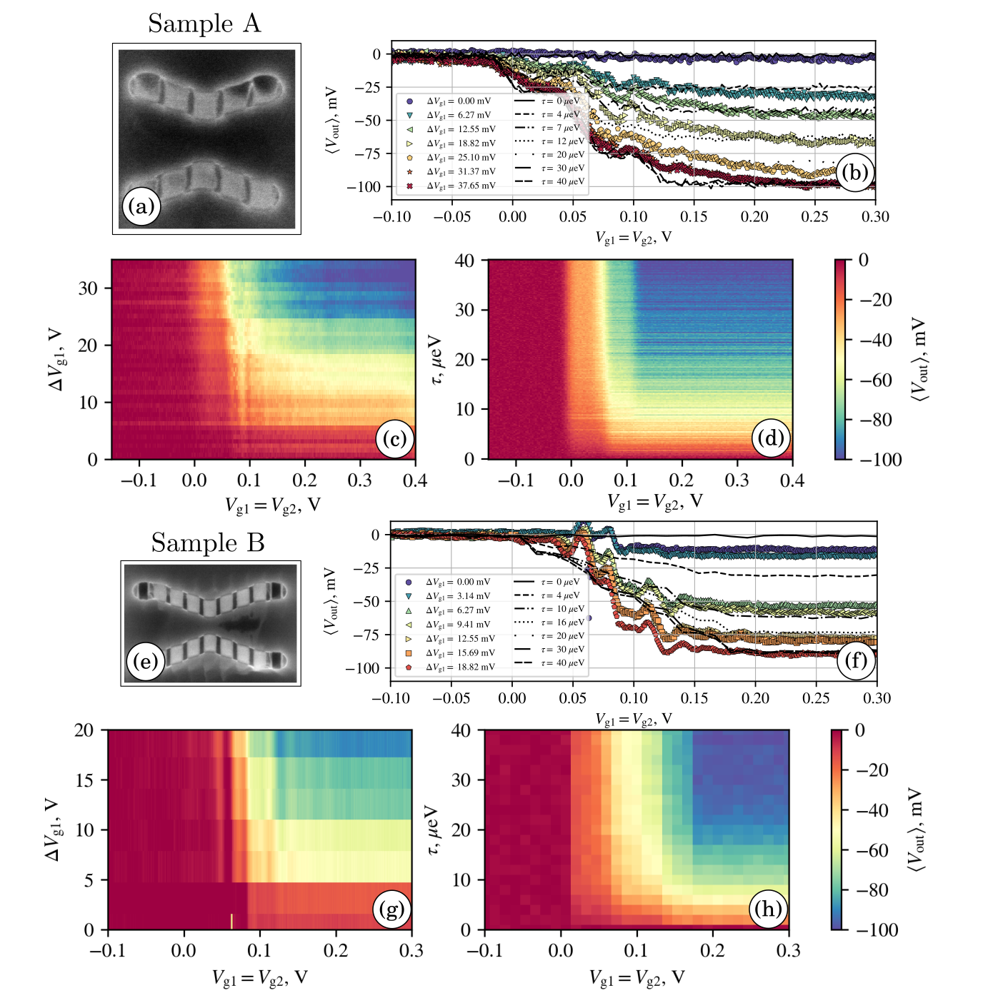
We can connect to the actual voltage measurements in our detectors using the transformation functions mV and mV, where is the experimentally measured voltage on structure , as we show in Fig. 3. Here, we plot the obtained as a function of the applied gate voltage in order to describe approximately the measured voltage drop. We use the transformation function obtained from QTCAD simulations. Moreover, to account for the effects of noise in the measurement, we use a Gaussian noise filter in our calculated output observable. That is we plot: , where with and , for both structures. Sweeping over and voltages in the experiment corresponds to sweeping over and in our model.
As a conclusion, we would like to highlight some key points of this work. Firstly, we showed that the resolution of our device is sensitive to single-electron injection within some variance induced by thermal noise due to the finite operating temperature. This shows that both the device and the incorporation of a metallic floating node with standard CCD circuitry are efficient in relevant quantum charge sensing applications. Moreover, the agreement between our simulations from QTCAD and MOAIM with the experimentally measured data further hints at the device behaving as an SEB and a QD forming under Gate 2. The predictions of the MOAIM are compatible both with the applied voltages and the QD geometry in the actual device and it captures effectively the most significant aspects of the experiment. These are the measured voltage at electron injection plateaus (quantized charge, Coulomb blockade), the stretching of the curves when the coupling between metallic node and the QD is varied and the average decrease in the variation between curve gaps .
On the other hand, there are some potentially interesting physics that our model does not capture. Some of these are the small "S" shaped bumps in the experimental data which are located where injection happens (more apparent in sample B) and the voltage-dependent drift in the experimental curves (more apparent in sample A). Finally, one can in principle go beyond the semi-classical rate-equation treatment presented above to include QD-lead entanglement effects Minarelli, Rigo, and Mitchell (2022), renormalization phenomena at low-temperatures, and spin-flip scattering producing more subtle quantum behavior such as the Kondo effect Mitchell, Logan, and Krishnamurthy (2011). We leave all of the aforementioned as interesting outlooks for future research.
Author Declarations
Conflict of interest
The authors have no conflicts to disclose.
Data availability
The data that support the findings of this study are available from the corresponding authors upon reasonable request.
References
- Nazarov and Blanter (2009) Y. V. Nazarov and Y. M. Blanter, Quantum Transport: Introduction to Nanoscience (Cambridge University Press, 2009).
- Yadav et al. (2022) P. Yadav, S. Chakraborty, D. Moraru, and A. Samanta, “Variable-barrier quantum coulomb blockade effect in nanoscale transistors,” Nanomaterials (Basel) 12, 4437 (2022).
- Goodnick and Bird (2003) S. Goodnick and J. Bird, “Quantum-effect and single-electron devices,” IEEE Transactions on Nanotechnology 2, 368–385 (2003).
- Anders et al. (2023) J. Anders, J. C. Bardin, I. Bashir, G. Billiot, E. Blokhina, S. Bonen, E. Charbon, J. Chiaverini, I. L. Chuang, C. Degenhardt, et al., “Cmos integrated circuits for the quantum information sciences,” IEEE transactions on quantum engineering (2023).
- Bashir et al. (2020) I. Bashir, E. Blokhina, A. Esmailiyan, D. Leipold, M. Asker, E. Koskin, P. Giounanlis, H. Wang, D. Andrade-Miceli, A. Sokolov, et al., “A single-electron injection device for CMOS charge qubits implemented in 22-nm FD-SOI,” IEEE Solid-State Circuits Letters 3, 206–209 (2020).
- Filmer et al. (2020) M. J. Filmer, T. A. Zirkle, J. Chisum, A. O. Orlov, and G. L. Snider, “Using single-electron box arrays for voltage sensing applications,” Applied Physics Letters 116, 213103 (2020).
- Power et al. (2022) C. Power, D. Andrade-Miceli, I. Bashir, M. Asker, D. Leipold, R. B. Staszewski, and E. Blokhina, “Modelling of electron injection and confinement in cryogenic 22-nm fd-soi quantum dot arrays,” in 2022 29th IEEE International Conference on Electronics, Circuits and Systems (ICECS) (IEEE, 2022) pp. 1–4.
- Oakes et al. (2023) G. A. Oakes, V. N. Ciriano-Tejel, D. F. Wise, M. A. Fogarty, T. Lundberg, C. Lainé, S. Schaal, F. Martins, D. J. Ibberson, L. Hutin, B. Bertrand, N. Stelmashenko, J. W. A. Robinson, L. Ibberson, A. Hashim, I. Siddiqi, A. Lee, M. Vinet, C. G. Smith, J. J. L. Morton, and M. F. Gonzalez-Zalba, “Fast high-fidelity single-shot readout of spins in silicon using a single-electron box,” Phys. Rev. X 13, 011023 (2023).
- Mihailescu et al. (2023) G. Mihailescu, A. Bayat, S. Campbell, and A. K. Mitchell, “Multiparameter critical quantum metrology with impurity probes,” (2023), arXiv:2311.16931 [quant-ph] .
- Mihailescu, Campbell, and Mitchell (2023) G. Mihailescu, S. Campbell, and A. K. Mitchell, “Thermometry of strongly correlated fermionic quantum systems using impurity probes,” Phys. Rev. A 107, 042614 (2023).
- Janesick et al. (1990) J. R. Janesick, T. S. Elliott, A. Dingiziam, R. A. Bredthauer, C. E. Chandler, J. A. Westphal, and J. E. Gunn, “New advancements in charge-coupled device technology: subelectron noise and 4096 x 4096 pixel ccds,” in Charge-Coupled Devices and Solid State Optical Sensors, Vol. 1242 (SPIE, 1990) pp. 223–237.
- Abramoff et al. (2019) O. Abramoff, L. Barak, I. M. Bloch, L. Chaplinsky, M. Crisler, A. Drlica-Wagner, R. Essig, J. Estrada, E. Etzion, G. Fernandez, et al., “Sensei: direct-detection constraints on sub-gev dark matter from a shallow underground run using a prototype skipper ccd,” Physical review letters 122, 161801 (2019).
- Tiffenberg et al. (2017) J. Tiffenberg, M. Sofo-Haro, A. Drlica-Wagner, R. Essig, Y. Guardincerri, S. Holland, T. Volansky, and T.-T. Yu, “Single-electron and single-photon sensitivity with a silicon skipper ccd,” Physical review letters 119, 131802 (2017).
- Child et al. (2022) T. Child, O. Sheekey, S. Lüscher, S. Fallahi, G. C. Gardner, M. Manfra, A. Mitchell, E. Sela, Y. Kleeorin, Y. Meir, and J. Folk, “Entropy measurement of a strongly coupled quantum dot,” Phys. Rev. Lett. 129, 227702 (2022).
- Han et al. (2022) C. Han, Z. Iftikhar, Y. Kleeorin, A. Anthore, F. Pierre, Y. Meir, A. K. Mitchell, and E. Sela, “Fractional entropy of multichannel kondo systems from conductance-charge relations,” Phys. Rev. Lett. 128, 146803 (2022).
- Hewson (1993) A. C. Hewson, The Kondo Problem to Heavy Fermions, Cambridge Studies in Magnetism (Cambridge University Press, 1993).
- (17) Nanoacademic Technologies Inc., “QTCAD finite-element-based simulation platform for quantum technology,” https://docs.nanoacademic.com/qtcad/theory/poisson/.
- Kittel (2004) C. Kittel, Introduction to solid state physics, 8th ed. (John Wiley & Sons, Nashville, TN, 2004).
- Kouwenhoven et al. (1997) L. P. Kouwenhoven, C. M. Marcus, P. L. McEuen, S. Tarucha, R. M. Westervelt, and N. S. Wingreen, “Electron transport in quantum dots,” in Mesoscopic electron transport (Springer, 1997) pp. 105–214.
- Shangguan et al. (2001) W. Shangguan, T. A. Yeung, Y. Yu, and C. Kam, “Quantum transport in a one-dimensional quantum dot array,” Physical Review B 63, 235323 (2001).
- Gurvitz (1998) S. Gurvitz, “Rate equations for quantum transport in multidot systems,” Physical Review B 57, 6602 (1998).
- Fransson and Råsander (2006) J. Fransson and M. Råsander, “Pauli spin blockade in weakly coupled double quantum dots,” Phys. Rev. B 73, 205333 (2006).
- Minarelli, Rigo, and Mitchell (2022) E. L. Minarelli, J. B. Rigo, and A. K. Mitchell, “Linear response quantum transport through interacting multi-orbital nanostructures,” (2022), arXiv:2209.01208 [cond-mat.str-el] .
- Mitchell, Logan, and Krishnamurthy (2011) A. K. Mitchell, D. E. Logan, and H. Krishnamurthy, “Two-channel kondo physics in odd impurity chains,” Physical Review B 84, 035119 (2011).