Enhanced interlayer electron transfer by surface treatments in mixed-dimensional van der Waals semiconductor heterostructures
Abstract
We investigate the excitonic species in WS2 monolayers transferred onto III-V semiconductor substrates with different surface treatments. When the III-V substrates were covered with amorphous native oxides, negatively charged excitons dominate the spectral weight in low-temperature near-resonance photoluminescence (PL) measurements. However, when the native oxides of the III-V substrates were reduced, neutral excitons begin to dominate the spectral weight, indicating a reduction in the electron density in the WS2 monolayers. The removal of the native oxides enhanced the electron transfer from the WS2 monolayer to the III-V substrate. In addition, an additional shoulder-like PL feature appeared 50 meV below the emission of neutral excitons, which can be attributed to the emission of localized excitons. When the III-V substrate surface was passivated by sulfur after the reduction of the native oxides, neutral excitons still dominated the spectral weight. However, the low energy PL shoulder disappeared again, suggesting the effective delocalization of excitons through the substrate surface passivation. Surface engineering of the semiconductor substrates for two-dimensional (2D) materials can provide a novel approach to control the carrier density of the 2D materials, to implement deterministic carrier localization or delocalization for the 2D materials, and to facilitate the interlayer transfer of charge, spin, and valley currents. These findings open the avenue for novel device concepts and phenomena in mixed-dimensional semiconductor heterostructures.
I Introduction
Since the isolation of graphene [1], a wide variety of two-dimensional (2D) van der Waals (vdW) materials have been studied over the past decades: a library of 2D vdW crystals has been expanded to semiconducting transition metal dichalcogenides (TMDCs) [2, 3, 4, 5], insulating hexagonal boron nitride (hBN) [6], and even ferromagnetic CrI3 [7] and Cr2Ge2Te6 [8], as well as ferroelectric and piezoelectric SnTe [9], SnS [10, 11], WTe2 [12], and -In2Se3 [13, 14, 15]. Importantly, such 2D vdW materials generally require a substrate to provide mechanical support, which at the same time significantly influences their properties. For example, the significant enhancement of the electronic properties of graphene encapsulated by high-quality hBN [6] emphasizes the importance of the substrate material. This means that the interface between 2D materials and substrates which are typically three-dimentional (3D) bulk becomes crucial for harnessing the potential characteristics of 2D materials.
Such 2D/3D heterostructures are promising platform for novel artificial material design. This is because dangling bond-free surfaces for 2D materials allow the stacking of constituent layers at desired sequences and angles, that can not be realized by epitaxial growth of 2D materials on 3D substrates. In particular, vdW heterostructures based on 3D III-V semiconductor and 2D TMDC are among promising platforms by taking advantage of high mobility and strong light absorption for III-V semiconductors and spin-valley coupling for TMDCs. Indeed, variety of state-of-the-art devices have been realized, incluiding a helicity-controllable spin light-emitting diodes [16], highly efficient solar cells [17], and ultrasensitive photodetectors [18, 19].
For these applications, charge and/or spin transfer between these 2D and 3D materials is critical in the efficiency of device operation. Interestingly, as will be shown in this paper, such interconnection across the interface is drastically modified only by controlling the surface of 3D materials. However, the effect of surface treatment itself on both electrical and optical properties of the 2D/3D heterostructures has not been discussed intensively. Therefore, in this study, we shed light on the surface treatment techniques and comprehensively discuss their effects on the optoelectrical properties of the 2D material.
We focused on monolayer WS2/III-V semiconductor heterostructures and demonstrates that reducing the native oxides of the III-V semiconductor enhances the electron transfer from the WS2 to the III-V substrate. Furthermore, passivating the reduced III-V substrate by sulfur effectively reduces the spectral weight of localized excitons.
II Sample fabrication procedure
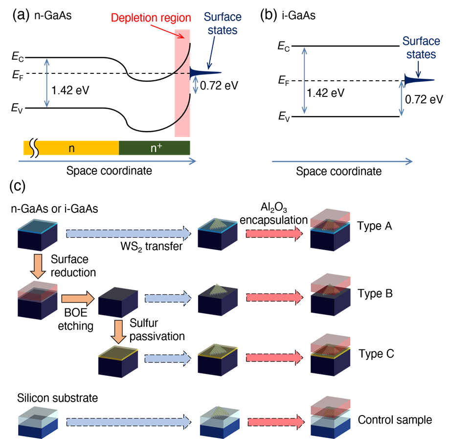
The III-V semiconductors used in this study were heavily -doped In0.04Ga0.96As and semi-insulating GaAs structures. The -doped structure is composed of a 20 nm -In0.04Ga0.96As layer ( cm-3), a 500 nm -In0.04Ga0.96As layer ( cm-3) and a 300 nm semi-insulating GaAs buffer layer, epitaxially grown on a (001) semi-insulating GaAs substrate. The bottom of the conduction band (CB) in the -In0.04Ga0.96As layer is below the Fermi level, while that in the -In0.04Ga0.96As layer is above the Fermi level. As shown in Fig. 1(a), since the surface Fermi level is at 0.72 eV above the top of the valence band (VB) [20], the Fermi level difference between the surface and bulk of the -In0.04Ga0.96As layer induces carrier depletion near the surface, resulting a significant band bending. On the other hand, the semi-insulating structure consists of nominally undoped (001) GaAs. As shown in Fig. 1(b), the surface Fermi level of this structure is also at 0.72 eV above the top of the VB [20]. Hereafter, the -type and semi-insulating structures are denoted as -GaAs and -GaAs, respectively.
As illustrated in Fig. 1(c), the - and -GaAs structures underwent three different surface treatments: Type A, B, and C. Type A samples were rinsed with acetone, ethanol and, deionized water, leaving their surface covered with amorphous native oxides. Type B samples underwent surface reduction through the self-cleaning effect by trimethylaluminum (TMA) vapors during atomic layer deposition (ALD) of Al2O3 [21, 22], after being rinsed with acetone, ethanol, and deionized water. The self-cleaning process consisted of 60 cycles of TMA pulse-purge sequences, which effectively removed a significant portion of the native oxides [21, 22]. Subsequently, a buffered oxide etchant (BOE) was used to etch the Al2O3 layers, leaving the III-V substrates unetched. Type C samples underwent sulfur passivation by immersion in a CH3CSNH2/NH4OH solution [23, 24], following degreasing with acetone, ethanol, and deionized water, as well as the above-mentioned surface reduction process. Highly crystalline WS2 monolayers synthesized using a NaCl-assisted chemical vapor deposition (CVD) method were then transferred onto the -GaAs and -GaAs structures using a polycarbonate-based clean transfer method. The samples were then encapsulated with an Al2O3 layer deposited by ALD to prevent physisorption of H2O and O2 molecules on the WS2 surface, which could otherwise destabilize the carrier density in WS2 [25].
As a control substrate, we used a silicon substrate consisting of thermally oxidized 300 nm SiO2/Si where the 300-nm-thick SiO2 layer prevents interlayer charge transfer between WS2 and Si.
III effect of surface treatment on substrate properties
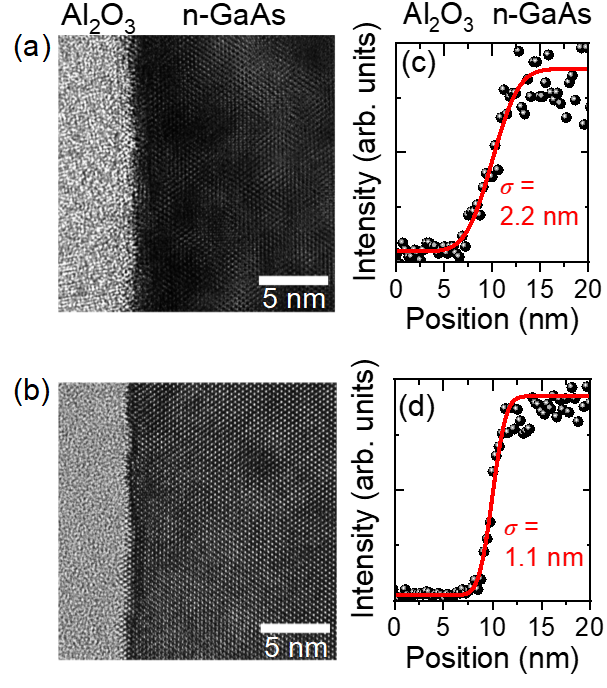
We first confirm that the self-cleaning effect occurs during the Type B and C surface treatments by comparing the samples processed with and without the multiple TMA purge sequences before Al2O3 deposition. Figures 2(a) and 2(b) show the transmission electron microscopy (TEM) images of the Al2O3/-GaAs interfaces with 1 cycle and 60 cycles of TMA pulse-purge secuences, respectively. Here, while a brighter region corresponds to the Al2O3 layer, a darker region corresponds to the -GaAs structure. Since the one pulse-purge sequence reduces only a small fraction of the native oxides [22], the interface shown in Fig. 2(a) is blurrier than that in Fig. 2(b).
For quantitative analysis of the interfacial roughness, we used TEM-coupled energy dispersive X-ray (EDX) spectroscopy to obtain atomic composition profiles for the regions shown in Figs. 2(a) and 2(b). The EDX line profiles are presented in Figs. 2(c) and 2(d), respectively. The sums of the EDX signals from the Ga and As L shells are represented by the black circles. The interfacial roughness is extracted using fits to a step-like function , shown by the red curves. Here, is the error function with as a variable, is step height, is background signal, is position, is center position, and is interfacial roughness. The interfacial roughness was improved from 2.2 to 1.1 nm after 60 cycles of TMA pulse-purge sequences, as shown in Fig. 2(d). This decrease in the interfacial roughness indicates the effective removal of the amorphous native oxides, which is consistent with the self-cleaning effect [21, 22].
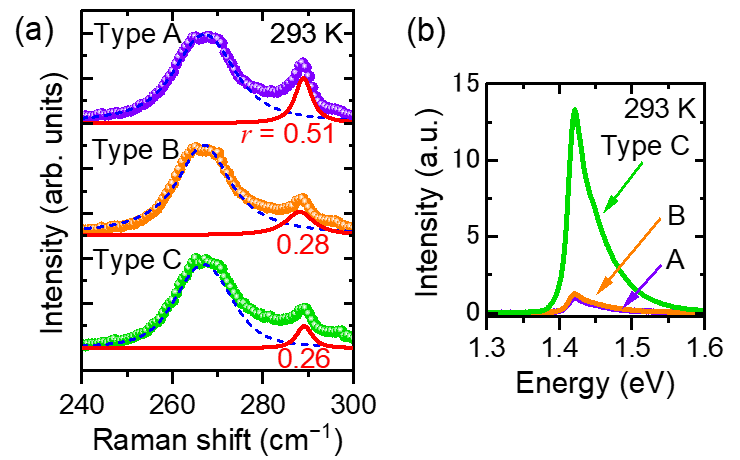
The difference due to the surface treatments can be also seen in the Raman spectra measured for the -GaAs structure. Figure 3(a) shows the Raman spectra for the -GaAs structure after transferring WS2 monolayer at room temperature in the backscattering configuration under 532 nm excitation. The laser penetration depth was estimated to be 124 nm and phonon signal near the -GaAs surfaces can be observed. Two distinct peaks at 288 and 268 cm-1 are attributed to the longitudinal optical (LO) phonon mode and the lower branch of the LO-phonon-plasmon-coupled (L-) mode, respectively [26, 27]. The L- mode originates from a un-depleted region and becomes prominent at high carrier density where the coupling between LO phonons and plasmons becomes important [26, 27, 28]. Based on its position, the L- mode originates from the un-depleted region in the -In0.04Ga0.96As layer, not in the -In0.04Ga0.96As layer. This suggests that charge depletion occurs in the heavily doped -In0.04Ga0.96As layer, allowing us to analyze the depletion region width using the intensity ratio between the LO and L- modes. It is important to note that Raman scattering from transverse optical phonons, which could spectrally overlap with the LO mode [29], is forbidden due to the (001) crystallographic orientation and the backscattering configuration [30]. This selection rule allows for a safe comparison of the intensity ratio , where and represent the integral intensities of the L- and LO modes, respectively. The integral intensities were determined using a Voigt fit for each peak. The values of decrease from 0.51 for Type A to 0.28 and 0.26 for Type B and C, respectively. This indicates that the self-cleaning and sulfur passivation processes have reduced the thickness of the depletion region. The reduction is attributed to the decrease in the number of surface states. When the density of surface states increases, more free electrons are trapped on the surface.
Figure 3(b) shows the PL spectra for -GaAs at room temperature under 2.21 eV excitation with a fixed excitation power. The PL centered at 1.42 eV is attributed to radiative recombination from the CB to the VB [31]. Importantly, the peak intensity of Type B showed a 1.25-fold increase compared to that of Type A. After the additional sulfur passivation process, Type C showed a substantial 13.3-fold increase of PL intensity compared to Type A. These facts suggest that non-radiative recombination pathways were reduced due to a decrease in the number of surface states. These results are consistent with those obtained by Raman spectroscopy [Fig. 3(a)]. It is worth noting that unlike the top layers of the -GaAs structure, the -GaAs structure is nominally undoped and thus the number of free carriers is insufficient to observe the L- mode. In the case of the -GaAs structure, the aforementioned sharp band bending repels photoexcited electrons into the bulk region. Thus, PL intensity is insensitive to the number of surface states.
IV Effect of surface treatment on heterostructure properties
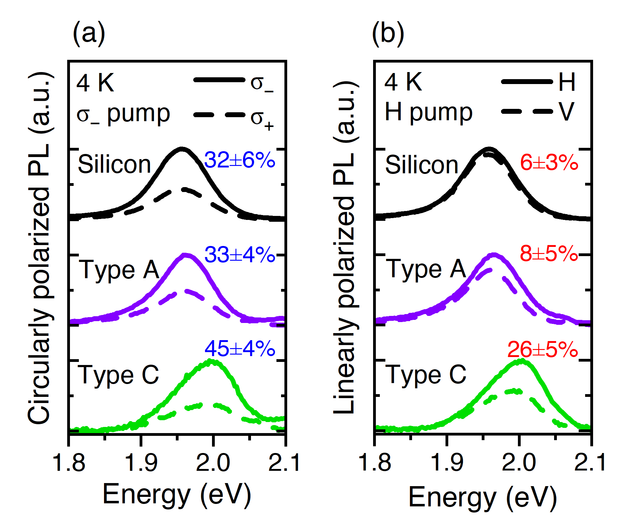
Polarization-resolved PL measurements were performed to assign the excitonic species in WS2 of the WS2/silicon, WS2/-GaAs and WS2/-GaAs samples. Both circularly and linearly polarized PL were measured under 2.21 eV excitation at a cryogenic temperature, , of 4 K. The excitation energy was near-resonant to the exciton PL energy. In the circularly polarized PL measurements, right-handed () and left-handed () circularly polarized PL were measured upon photoexcitation of the K valley by polarized light, following the spin-valley optical selection rule [32, 33, 34, 35, 36, 37]. In the linearly polarized PL measurements, on the other hand, horizontal (H) and vertical (V) linearly polarized PL were measured upon photoexcitation of both K and K’ valleys by H polarized light. To ensure reliable analysis of neutral and charged excitons, a combination of circularly and linearly polarized PL measurements was used instead of peak deconvolution. This approach excludes the effect of peak shifts that may be caused by changes in dielectric screening due to surface treatment of the III-V substrate [38, 39].
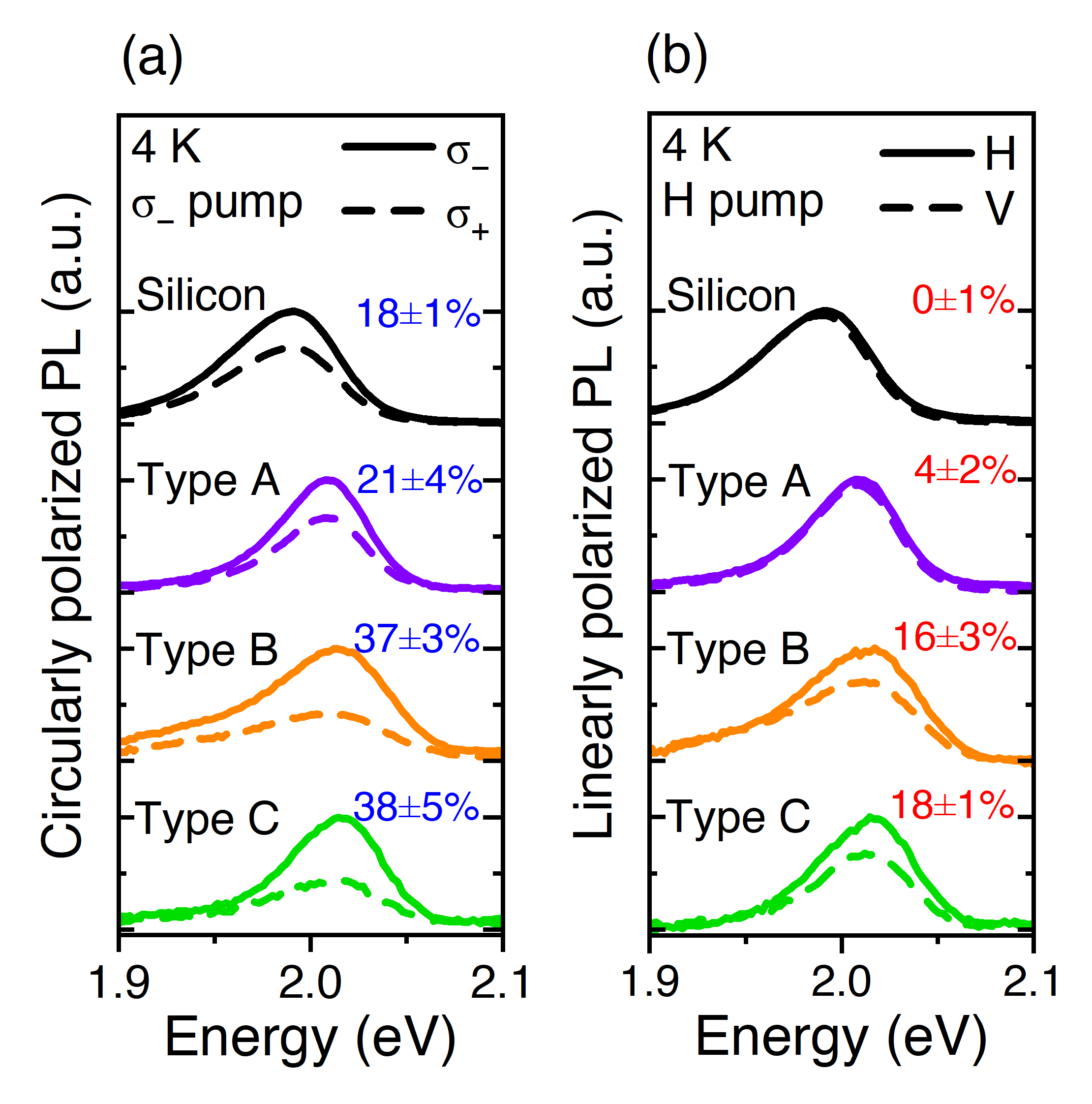
Figure 4(a) shows representative circularly polarized PL spectra for the WS2/silicon (black) and the WS2/-GaAs with Type A, B, and C treatments (purple, orange, and green). In each pair of spectra, the solid and dashed curves represent and polarized PL spectra, respectively. Degree of circular polarization for each sample is summarized in Table 1 where is the intensity of polarized PL averaged within meV around the peak energy. The large independent of the substrate conditions means all samples realized excitonic valley polarization [32, 33, 34, 35, 36, 37]. In other words, depolarization pathways through the electron-hole (e-h) Coulomb exchange interaction [37, 40] and simultaneous intervalley scattering of electrons and holes by two longitudinal acoustic (LA) phonons [41, 42, 43] were effectively suppressed. This is indeed plausible because the broken inversion symmetry , where represents the crystal momentum, should still persist. This is in contrast to the case of bilayer TMDCs [33].
| Substrate | ||||
|---|---|---|---|---|
| Silicon | ||||
| Type A | ||||
| Type B | ||||
| Type C |
Figure 4(b) shows linearly polarized PL spectra for the WS2/silicon (black) and the WS2/-GaAs with Type A, B, and C treatments (purple, orange, and green) measured at the same spot as in Fig. 4(a). In each pair of spectra, the solid and dashed curves represent H and V polarized PL spectra, respectively. Degree of linear polarization for each sample is summarized in Table 1 where is the intensity of H(V) polarized PL averaged within meV around the peak energy. By analyzing changes in , we assign the dominant excitonic species that contribute the observed PL lines as follows.
Previous studies have shown that in low carrier density, the PL spectrum of WS2 is dominated by a Coulomb-bound electron-hole pair, known as a neutral exciton (X0) [35, 36]. At K, where our measurements were performed, PL emission from X0 under linearly polarized excitation is considered to show as follows. A linear superposition of K and K’ valleys created by linearly polarized light emits the same linearly polarized light if the recombination lifetime is shorter than the valley decoherence time. In our case, this situation is plausible since the valley depolarization was effectively suppressed untill recombination as confirmed from under the circularly polarized excitation [Fig. 4(a)]. In higher carrier density, on the other hand, X0 captures the excess electron or hole, and forms negatively or positively charged excitons (X- or X+), respectively. The PL from both X- and X+ are not linearly polarized (i.e., ) even if valley depolarization is suppressed. This is because the optical transition is allowed for circularly polarized light rather than linearly polarized light due to the eigenstate mixing of excitonic state induced by the exchange interaction [35, 37]. Therefore, a larger indicates that X0 is dominant.
For the WS2/silicon samples, X- or X+ dominates the spectral weight since was observed. The small values agree well with the -type behavior of CVD-grown WS2 monolayers due to the energetically preferred formation of sulfur vacancies [44]. Therefore, we assign X- as the dominant excitonic species in the WS2/silicon samples.
For the Type A WS2/-GaAs samples, relatively small suggests that either X- or X+ dominates the spectral weight. In addition to the fact that the CVD-grown WS2 monolayers behave -type as mentioned above [44], the energy gap of native oxides 4 eV [45] is large enough to disturb the electron transfer from the WS2 to the substrate even after the heterostructure fabrication. Furthermore, the heavily -doped substrate cannot provide sufficient holes to WS2. Therefore, X- still dominates the spectrum from Type A samples similar to the WS2/silicon samples.
On the other hand, the Type B and C WS2/-GaAs samples exhibited relatively large , and , respectively. This indicates X0 emission increased, suggesting a reduction in electron density compared to the cases of the WS2/silicon and Type A WS2/-GaAs samples. Therefore the self-cleaning effect due to the TMA pulse-purge sequences successfully removed the native oxides on the substrate surface and thus lowered the energy barrier between WS2 and the substrate.
The impact of sulfur passivation can be seen in a PL shoulder at around 1.95 eV that is present in Type B but absent in Type A and C [Figs. 4(a) and 4(b)]. This shoulder was reproduced in all Type B samples measured, not just the Type B sample shown in Fig. 4. As has been reported in MoS2/GaAs heterostructures [46], the PL shoulder is considered to originate from exciton localization or interfacial charge trap. The presence of the PL shoulder in the WS2/Type B -GaAs samples and the absence of such shoulder in the WS2/Type C -GaAs samples suggest that sulfur passivation plays a significant role in reducing exciton localization or interfacial charge trap in monolayer WS2. This is consistent with the broadest LO peak for Type B -GaAs in Fig. 3(a) since the dangling bonds can be the origin of surface states which is in principle disordered and leads to broadening of Raman peak. Consequently, the use of the III-V substrates with well-controlled surface states plays a significant role for both localization and delocalization of electrons in monolayer WS2/III-V semiconductor heterostructures.
The underlying mechanism behind the change in the excitonic species is discussed below. The topmost -In0.04Ga0.96As layer of the -GaAs structure is -doped and has a thin depletion region. The modification in both surface states and depletion regions may be dominant factors. To investigate these mechanisms, the semi-insulating -GaAs structures were used to exclude the effect of the depletion regions.
| Substrate | ||||
| Silicon | ||||
| Type A | ||||
| Type B | NA | NA | ||
| Type C |
Figure 5(a) shows representative circularly polarized PL spectra for the WS2/silicon and WS2/-GaAs samples with different surface treatments. All samples show a clear difference between the and components, indicating effective suppression of the e-h Coulomb exchange [37, 40] and LA phonon [41, 42, 43] depolarization pathways. Similar to the -GaAs cases, this fact allows to identify the excitonic species through the degree of linear polarization.
Figure 5(b) shows the linearly polarized PL spectra measured at the same spot as in Fig. 5(a) where H (V) polarized PL are indicated as solid (dashed) curves. As summarized in Table 2, is larger in the Type C WS2/-GaAs samples (green) compared to the WS2/silicon (black) and Type A WS2/-GaAs samples (purple). This suggests a lower electron density in the Type C WS2/-GaAs samples compared to the WS2/silicon and Type A WS2/-GaAs samples, similar to the -GaAs case. It should be noted that the batches used to synthesize WS2 were different in Figs. 4 and 5. This must lead to the batch-to-batch difference in the quality of the WS2 monolayers, including defect and carrier density, resulting in the difference in PL polarization degrees, for example, as seen in WS2/silicon samples. However, quantitative comparison within the same figure should make sense.
Regardless of the substrate doping concentrations, the Type A samples exhibit lower values of , i.e., a dominance of X- over X0. In contrast, the Type B and C samples exhibit an increased spectral weight of X0. Namely, the reduction in the electron density in WS2 is observed regardless of the presence or absence of depletion regions near the surface of the III-V semiconductors. This suggests that the space charges in the depletion regions do not play a dominant role in reducing the electron density in WS2. However, the Type B and C WS2/-GaAs samples exhibit similar regardless of the reduction of surface states. This suggests that the space charges at the surface states do not play a significant role. Because the space charges in the depletion regions and at the surface do not play a role for changing the carrier density in monolayer WS2, we conclude that the electron transfer from the CB of monolayer WS2 to that of III-V semiconductor plays a role in reducing the carrier density in the WS2/Type B -GaAs and WS2/Type C -GaAs samples.
V conclusion
We focused on WS2/-GaAs and WS2/-GaAs heterostructures and investigated the effect of surface treatments for the III-V substrates on the excitonic species in the WS2 monolayer. The PL emission from the WS2 monolayers was dominated by the X- feature in the WS2/untreated -GaAs and WS2/untreated -GaAs samples, regardless of the substrate doping concentrations. However, in the case of the WS2/surface-reduced -GaAs, WS2/sulfur-passivated -GaAs and WS2/sulfur-passivated -GaAs samples, the X0 feature dominated the PL spectra, indicating a reduced electron density in the WS2 monolayers. The removal of the native oxides may enhance the electron transfer from the WS2 monolayer to the III-V substrates. This means that the relatively low spin injection efficiency, for example, from (Ga,Mn)As to WS2 monolayer can be improved by removing the native oxides of the (Ga,Mn)As substrate [16]. Furthermore, for the WS2/surface-reduced -GaAs samples, an additional PL shoulder appears at 50 meV lower than the X0 feature, suggesting exciton localization or interfacial charge trap. However, such a PL shoulder was absent in the WS2/sulfur-passivated -GaAs samples. Therefore, the surface passivation of the III-V substrate may play an important role in suppressing exciton localization or interfacial charge trap in the WS2 monolayer, which can lead to high mobility devices [6]. These findings could lead to novel device concepts, including gate-free doping and deterministic carrier localization or delocalization for 2D materials.
Supplementary Material
The supplementary material contains detailed procedures for the surface processing, the WS2 growth and transfer, and the PL measurements.
Acknowledgements.
T.O. and K.K. acknowledge the financial support from the Graduate Program in Spintronics (GP-Spin) at Tohoku University. T.O. was financially supported by the JST-SPRING program (Grant No. JPMJSP2114). T.O. acknowledges the technological support from Dr. Kosei Kobayashi at the Graduate School of Engineering, Tohoku University. This work was supported by the JSPS KAKENHI program (Grant No. 21H04647) and the JST-FOREST and CREST programs (Grant Nos. JPMJFR203C and JPMJCR22C2).AUTHOR DECLARATIONS
Conflict of Interest
The authors have no conflicts to disclose.
Author Contributions
Takeshi Odagawa: Data curation (lead); Formal analysis (lead); Investigation (lead); Methodology (equal); Resources (lead); Validation (lead); Visualization (lead); Writing - original draft (lead); Writing - review & editing (equal). Sota Yamamoto: Formal analysis (equal); Validation (equal); Writing - review & editing (equal). Chaoliang Zhang: Methodology (equal); Resources (equal); Formal analysis (equal); Validation (equal); Writing - review & editing (equal). Kazuki Koyama: Resources (equal); Validation (equal); Writing - review & editing (equal). Jun Ishihara: Formal analysis (equal); Validation (equal); Writing - review & editing (equal). Giacomo Mariani: Validation (equal); Writing - review & editing (equal). Yoji Kunihashi: Validation (equal); Writing - review & editing (equal). Haruki Sanada: Validation (equal); Writing - review & editing (equal). Junsaku Nitta: Conceptualization (equal); Project administration (equal); Writing - review & editing (equal). Makoto Kohda: Conceptualization (lead); Methodology (lead); Project administration (lead); Writing - review & editing (lead).
Data Availability Statement
The data that support the findings of this study are available from the corresponding author upon reasonable request.
References
- Novoselov et al. [2016] K. S. Novoselov, A. Mishchenko, A. Carvalho, and A. H. C. Neto, “2D materials and van der Waals heterostructures,” Science 353, aac9439 (2016), https://www.science.org/doi/pdf/10.1126/science.aac9439 .
- Novoselov et al. [2005] K. S. Novoselov, D. Jiang, F. Schedin, T. J. Booth, V. V. Khotkevich, S. V. Morozov, and A. K. Geim, “Two-dimensional atomic crystals,” Proceedings of the National Academy of Sciences 102, 10451–10453 (2005), https://www.pnas.org/doi/pdf/10.1073/pnas.0502848102 .
- Mak et al. [2010] K. F. Mak, C. Lee, J. Hone, J. Shan, and T. F. Heinz, “Atomically Thin : A New Direct-Gap Semiconductor,” Phys. Rev. Lett. 105, 136805 (2010).
- Splendiani et al. [2010] A. Splendiani, L. Sun, Y. Zhang, T. Li, J. Kim, C.-Y. Chim, G. Galli, and F. Wang, “Emerging photoluminescence in monolayer MoS2,” Nano letters 10, 1271–1275 (2010).
- Manzeli et al. [2017] S. Manzeli, D. Ovchinnikov, D. Pasquier, O. V. Yazyev, and A. Kis, “2D transition metal dichalcogenides,” Nature Reviews Materials 2, 17033 (2017).
- Dean et al. [2010] C. R. Dean, A. F. Young, I. Meric, C. Lee, L. Wang, S. Sorgenfrei, K. Watanabe, T. Taniguchi, P. Kim, K. L. Shepard, and J. Hone, “Boron nitride substrates for high-quality graphene electronics,” Nature Nanotechnology 5, 722–726 (2010).
- Huang et al. [2017] B. Huang, G. Clark, E. Navarro-Moratalla, D. R. Klein, R. Cheng, K. L. Seyler, D. Zhong, E. Schmidgall, M. A. McGuire, D. H. Cobden, W. Yao, D. Xiao, P. Jarillo-Herrero, and X. Xu, “Layer-dependent ferromagnetism in a van der Waals crystal down to the monolayer limit,” Nature 546, 270–273 (2017).
- Gong et al. [2017] C. Gong, L. Li, Z. Li, H. Ji, A. Stern, Y. Xia, T. Cao, W. Bao, C. Wang, Y. Wang, Z. Q. Qiu, R. J. Cava, S. G. Louie, J. Xia, and X. Zhang, “Discovery of intrinsic ferromagnetism in two-dimensional van der Waals crystals,” Nature 546, 265–269 (2017).
- Chang et al. [2016] K. Chang, J. Liu, H. Lin, N. Wang, K. Zhao, A. Zhang, F. Jin, Y. Zhong, X. Hu, W. Duan, Q. Zhang, L. Fu, Q.-K. Xue, X. Chen, and S.-H. Ji, “Discovery of robust in-plane ferroelectricity in atomic-thick SnTe,” Science 353, 274–278 (2016), https://www.science.org/doi/pdf/10.1126/science.aad8609 .
- Khan et al. [2020] H. Khan, N. Mahmood, A. Zavabeti, A. Elbourne, M. A. Rahman, B. Y. Zhang, V. Krishnamurthi, P. Atkin, M. B. Ghasemian, J. Yang, G. Zheng, A. R. Ravindran, S. Walia, L. Wang, S. P. Russo, T. Daeneke, Y. Li, and K. Kalantar-Zadeh, “Liquid metal-based synthesis of high performance monolayer SnS piezoelectric nanogenerators,” Nature Communications 11, 3449 (2020).
- Higashitarumizu et al. [2020] N. Higashitarumizu, H. Kawamoto, C.-J. Lee, B.-H. Lin, F.-H. Chu, I. Yonemori, T. Nishimura, K. Wakabayashi, W.-H. Chang, and K. Nagashio, “Purely in-plane ferroelectricity in monolayer SnS at room temperature,” Nature Communications 11, 2428 (2020).
- Fei et al. [2018] Z. Fei, W. Zhao, T. A. Palomaki, B. Sun, M. K. Miller, Z. Zhao, J. Yan, X. Xu, and D. H. Cobden, “Ferroelectric switching of a two-dimensional metal,” Nature 560, 336–339 (2018).
- Ding et al. [2017] W. Ding, J. Zhu, Z. Wang, Y. Gao, D. Xiao, Y. Gu, Z. Zhang, and W. Zhu, “Prediction of intrinsic two-dimensional ferroelectrics in In2Se3 and other III2-VI3 van der Waals materials,” Nature Communications 8, 14956 (2017).
- Zhou et al. [2017] Y. Zhou, D. Wu, Y. Zhu, Y. Cho, Q. He, X. Yang, K. Herrera, Z. Chu, Y. Han, M. C. Downer, H. Peng, and K. Lai, “Out-of-Plane Piezoelectricity and Ferroelectricity in Layered -In2Se3 Nanoflakes,” Nano Letters 17, 5508–5513 (2017).
- Xue et al. [2018] F. Xue, W. Hu, K.-C. Lee, L.-S. Lu, J. Zhang, H.-L. Tang, A. Han, W.-T. Hsu, S. Tu, W.-H. Chang, C.-H. Lien, J.-H. He, Z. Zhang, L.-J. Li, and X. Zhang, “Room-Temperature Ferroelectricity in Hexagonally Layered -In2Se3 Nanoflakes down to the Monolayer Limit,” Advanced Functional Materials 28, 1803738 (2018), https://onlinelibrary.wiley.com/doi/pdf/10.1002/adfm.201803738 .
- Ye et al. [2016] Y. Ye, J. Xiao, H. Wang, Z. Ye, H. Zhu, M. Zhao, Y. Wang, J. Zhao, X. Yin, and X. Zhang, “Electrical generation and control of the valley carriers in a monolayer transition metal dichalcogenide,” Nature Nanotechnology 11, 598–602 (2016).
- Lin et al. [2015] S. Lin, X. Li, P. Wang, Z. Xu, S. Zhang, H. Zhong, Z. Wu, W. Xu, and H. Chen, “Interface designed MoS2/GaAs heterostructure solar cell with sandwich stacked hexagonal boron nitride,” Scientific Reports 5, 15103 (2015).
- Jia et al. [2020] C. Jia, X. Huang, D. Wu, Y. Tian, J. Guo, Z. Zhao, Z. Shi, Y. Tian, J. Jie, and X. Li, “An ultrasensitive self-driven broadband photodetector based on a 2d-ws2/gaas type-ii zener heterojunction,” Nanoscale 12, 4435–4444 (2020).
- Li et al. [2020] K. Li, W. Wang, J. Li, W. Jiang, M. Feng, and Y. He, “High-responsivity, self-driven photodetectors based on monolayer WS2/GaAs heterojunction,” Photonics Research 8, 1368 (2020).
- Shen et al. [1990] H. Shen, M. Dutta, L. Fotiadis, P. G. Newman, R. P. Moerkirk, W. H. Chang, and R. N. Sacks, “Photoreflectance study of surface Fermi level in GaAs and GaAlAs,” Applied Physics Letters 57, 2118–2120 (1990), https://pubs.aip.org/aip/apl/article-pdf/57/20/2118/8996261/2118_1_online.pdf .
- Hinkle et al. [2008] C. L. Hinkle, A. M. Sonnet, E. M. Vogel, S. McDonnell, G. J. Hughes, M. Milojevic, B. Lee, F. S. Aguirre-Tostado, K. J. Choi, H. C. Kim, J. Kim, and R. M. Wallace, “GaAs interfacial self-cleaning by atomic layer deposition,” Applied Physics Letters 92, 071901 (2008), https://pubs.aip.org/aip/apl/article-pdf/doi/10.1063/1.2883956/14080480/071901_1_online.pdf .
- Lee et al. [2009] H. D. Lee, T. Feng, L. Yu, D. Mastrogiovanni, A. Wan, T. Gustafsson, and E. Garfunkel, “Reduction of native oxides on GaAs during atomic layer growth of Al2O3,” Applied Physics Letters 94, 222108 (2009), https://pubs.aip.org/aip/apl/article-pdf/doi/10.1063/1.3148723/14414518/222108_1_online.pdf .
- Lu et al. [1996] E. D. Lu, F. P. Zhang, S. H. Xu, X. J. Yu, P. S. Xu, Z. F. Han, F. Q. Xu, and X. Y. Zhang, “A sulfur passivation for GaAs surface by an organic molecular, CH3CSNH2 treatment,” Applied Physics Letters 69, 2282–2284 (1996), https://pubs.aip.org/aip/apl/article-pdf/69/15/2282/10167538/2282_1_online.pdf .
- Petrovykh, Long, and Whitman [2005] D. Y. Petrovykh, J. P. Long, and L. J. Whitman, “Surface passivation of InAs(001) with thioacetamide,” Applied Physics Letters 86, 242105 (2005), https://pubs.aip.org/aip/apl/article-pdf/doi/10.1063/1.1946182/13930434/242105_1_online.pdf .
- Tongay et al. [2013] S. Tongay, J. Zhou, C. Ataca, J. Liu, J. S. Kang, T. S. Matthews, L. You, J. Li, J. C. Grossman, and J. Wu, “Broad-Range Modulation of Light Emission in Two-Dimensional Semiconductors by Molecular Physisorption Gating,” Nano Letters 13, 2831–2836 (2013).
- Yokota [1961] I. Yokota, “On the Coupling between Optical Lattice Vibrations and Carrier Plasma Oscillations in Polar Semiconductors,” Journal of the Physical Society of Japan 16, 2075–2075 (1961), https://doi.org/10.1143/JPSJ.16.2075 .
- Varga [1965] B. B. Varga, “Coupling of Plasmons to Polar Phonons in Degenerate Semiconductors,” Phys. Rev. 137, A1896–A1902 (1965).
- Farrow, Sandroff, and Tamargo [1987] L. A. Farrow, C. J. Sandroff, and M. C. Tamargo, “Raman scattering measurements of decreased barrier heights in GaAs following surface chemical passivation,” Applied Physics Letters 51, 1931–1933 (1987), https://pubs.aip.org/aip/apl/article-pdf/51/23/1931/7764232/1931_1_online.pdf .
- Raman et al. [2023] R. Raman, A. Pandey, S. Dalal, S. Tyagi, and S. Kumar, “Polarized Raman scattering of (112) oriented GaAs and ZnTe crystals,” Applied Physics A 129, 164 (2023).
- Hayes and Loudon [1978] W. Hayes and R. Loudon, Scattering of Light by Crystals, Wiley-Interscience publication (Wiley, 1978).
- Tajima [1988] M. Tajima, “Characterization of semi-insulating GaAs wafers by room-temperature EL2-related photoluminescence,” Applied Physics Letters 53, 959–961 (1988), https://pubs.aip.org/aip/apl/article-pdf/53/11/959/7767035/959_1_online.pdf .
- Zeng et al. [2012] H. Zeng, J. Dai, W. Yao, D. Xiao, and X. Cui, “Valley polarization in MoS2 monolayers by optical pumping,” Nature Nanotechnology 7, 490–493 (2012).
- Mak et al. [2012] K. F. Mak, K. He, J. Shan, and T. F. Heinz, “Control of valley polarization in monolayer MoS2 by optical helicity,” Nature Nanotechnology 7, 494–498 (2012).
- Cao et al. [2012] T. Cao, G. Wang, W. Han, H. Ye, C. Zhu, J. Shi, Q. Niu, P. Tan, E. Wang, B. Liu, and J. Feng, “Valley-selective circular dichroism of monolayer molybdenum disulphide,” Nature Communications 3, 887 (2012).
- Jones et al. [2013] A. M. Jones, H. Yu, N. J. Ghimire, S. Wu, G. Aivazian, J. S. Ross, B. Zhao, J. Yan, D. G. Mandrus, D. Xiao, W. Yao, and X. Xu, “Optical generation of excitonic valley coherence in monolayer WSe2,” Nature Nanotechnology 8, 634–638 (2013).
- Hsu et al. [2015] W.-T. Hsu, Y.-L. Chen, C.-H. Chen, P.-S. Liu, T.-H. Hou, L.-J. Li, and W.-H. Chang, “Optically initialized robust valley-polarized holes in monolayer WSe2,” Nature Communications 6, 8963 (2015).
- Xiao et al. [2012] D. Xiao, G.-B. Liu, W. Feng, X. Xu, and W. Yao, “Coupled Spin and Valley Physics in Monolayers of and Other Group-VI Dichalcogenides,” Phys. Rev. Lett. 108, 196802 (2012).
- Lin et al. [2014] Y. Lin, X. Ling, L. Yu, S. Huang, A. L. Hsu, Y.-H. Lee, J. Kong, M. S. Dresselhaus, and T. Palacios, “Dielectric Screening of Excitons and Trions in Single-Layer MoS2,” Nano Letters 14, 5569–5576 (2014).
- Raja et al. [2017] A. Raja, A. Chaves, J. Yu, G. Arefe, H. M. Hill, A. F. Rigosi, T. C. Berkelbach, P. Nagler, C. Schüller, T. Korn, C. Nuckolls, J. Hone, L. E. Brus, T. F. Heinz, D. R. Reichman, and A. Chernikov, “Coulomb engineering of the bandgap and excitons in two-dimensional materials,” Nature Communications 8, 15251 (2017).
- Yu et al. [2014] H. Yu, G.-B. Liu, P. Gong, X. Xu, and W. Yao, “Dirac cones and Dirac saddle points of bright excitons in monolayer transition metal dichalcogenides,” Nature Communications 5, 3876 (2014).
- Asakura et al. [2021] E. Asakura, T. Odagawa, M. Suzuki, S. Karube, J. Nitta, and M. Kohda, “Intravalley scattering probed by excitation energy dependence of valley polarization in monolayer MoS2,” Journal of Physics D: Applied Physics 54, 485304 (2021).
- Kioseoglou et al. [2016] G. Kioseoglou, A. T. Hanbicki, M. Currie, A. L. Friedman, and B. T. Jonker, “Optical polarization and intervalley scattering in single layers of MoS2 and MoSe2,” Scientific Reports 6, 25041 (2016).
- Tornatzky, Kaulitz, and Maultzsch [2018] H. Tornatzky, A.-M. Kaulitz, and J. Maultzsch, “Resonance Profiles of Valley Polarization in Single-Layer and ,” Phys. Rev. Lett. 121, 167401 (2018).
- Amani et al. [2015] M. Amani, D.-H. Lien, D. Kiriya, J. Xiao, A. Azcatl, J. Noh, S. R. Madhvapathy, R. Addou, S. KC, M. Dubey, K. Cho, R. M. Wallace, S.-C. Lee, J.-H. He, J. W. Ager, X. Zhang, E. Yablonovitch, and A. Javey, “Near-unity photoluminescence quantum yield in MoS2,” Science 350, 1065–1068 (2015), https://www.science.org/doi/pdf/10.1126/science.aad2114 .
- Mikoushkin et al. [2018] V. M. Mikoushkin, V. V. Bryzgalov, S. Y. Nikonov, A. P. Solonitsyna, and D. E. Marchenko, “Composition and band structure of the native oxide nanolayer on the ion beam treated surface of the gaas wafer,” Semiconductors 52, 593–596 (2018).
- Rojas-Lopez et al. [2021] R. R. Rojas-Lopez, J. C. Brant, M. S. O. Ramos, T. H. L. G. Castro, M. H. D. Guimarães, B. R. A. Neves, and P. S. S. Guimarães, “Photoluminescence and charge transfer in the prototypical 2D/3D semiconductor heterostructure MoS2/GaAs,” Applied Physics Letters 119, 233101 (2021), https://pubs.aip.org/aip/apl/article-pdf/doi/10.1063/5.0068548/13032865/233101_1_online.pdf .