On the Path to High-temperature Josephson Multi-junction Devices
Abstract
We report our progress in the high-temperature superconductor (HTS) Josephson junction fabrication process founded on using a focused helium ion beam damaging technique and discuss the expected device performance attainable with the HTS multi-junction device technology. Both the achievable high value of characteristic voltage of Josephson junctions and the ability to design a large number of arbitrary located Josephson junctions allow narrowing the existing gap in design abilities for LTS and HTS circuits even with using a single YBCO film layer. A one-layer topology of active electrically small antenna is suggested and its voltage response characteristics are considered.
I Introduction
Superconductive electronics technologies leverage the distinctive macroscopic quantum phenomena exhibited by superconductors. These phenomena include superconductivity, magnetic flux quantization, and the effect of macroscopic quantum interference and Josephson effect [1, 2, 3], which are applicable across a wide range of frequencies from direct current (dc) to very high frequencies. The performance of the Josephson junctions deteriorates at frequencies higher than the characteristic Josephson junction frequency
| (1) |
where , and are the junction characteristic voltage, critical current, and resistance in the normal state, respectively, and represents the flux quantum. can reach hundreds of gigahertz and beyond. In addition, losses in superconductors remain low until reaching the gap frequency [3] (for example, the gap frequency of Nb is about ). The various superconductive electronics devices have been well developed [3] with some characteristics, which are difficult to attain using semiconductive electronic circults. The characteristics also promote a diverse range of digital and mixed-signal superconductive circuits, namely analog-to-digital converters (ADC) [4, 5, 6, 7, 8] and integrated digital circuits [9], including prototypes of microprocessors [10, 11, 12] , which can operate at frequencies with tens of gigahertz and even higher [13] These devices are powered by the Rapid Single Flux Quantum (RSFQ) logic [14, 15, 16, 17, 18, 19, 20, 21, 22], which operates using single flux quanta of magnetic flux for data signals and clock. In the RSFQ circuits, a single switching event of an overdamped Josephson junction (at , where is the capacitance of a junction [4]) with a typical consumes an extremely low energy of . Moreover, the switching time of the junction is about , allowing for clock frequencies in the hundreds of gigahertz range (e.g. see [13]).
Multiple Josephson junction devices can essentially improve the sensitivity and bandwidth of superconducting analog devices. Among them are SQUID-based array amplifiers [23], traveling wave parametric amplifiers [24, 25, 26, 27], as well as Superconducting Quantum Filters (SQIFs) [28, 29] and Superconducting Quantum Arrays (SQAs) [30] allowing implementation of highly sensitive active electrically small antennas (ESAs) capable of providing both the reception and amplification of an incident electromagnetic wave [31, 32]. Such broadband ESAs can improve overall performance of superconductive broadband digital-rf receivers based on direct signal digitization allowing then digital extraction of customizable sub-bands [33, 34]. As reported in [35, 36, 37], the receivable signal frequency can be ranged from VHF to K frequency bands.
These advances in the superconductive electronics have been achieved mainly by the use of low-temperature superconductors (LTS) and first of all a niobium fabrication process based on using tunnel Josephson junctions [3] with aluminum oxide barrier (e.g. see [38]). The implementation of high-temperature superconductor (HTS) devices, other than the simplest ones containing only a few Josephson junctions, poses a stiff challenge because of substantial design restrictions within the grain-boundary junction fabrication techniques (with either bi-crystal or step-edge or ramp-edge junctions) [3] which have been generally used until now. In spite of that, much simpler array-type HTS structures but composed of great deal of Josephson junctions were nevertheless realized using fabrication technique of step-edge Josephson junctions [39]. Such a SQIF-like 2D network containing in whole 54000 SQUIDs showed a magnetic field to voltage transfer function with a central peak value of approximately and a highly linear central peak portion around [39].
About a decade ago, an ion damaging technique was proposed to perform a controllable local suppression of superconducting properties of HTS films down to metallic or even to dielectric properties. When a focused ion beam is used, it enables forming a narrow barrier across a superconducting strip to realize a weak link between the strip parts and hence a Josephson junction with characteristics depending on irradiation dose [40]. Such a technique provides basis for a highly promising fabrication process enabling creation of high-quality multi-junction HTS devices. In fact, one can refer to [41, 42, 43] where the ion-beam damaging impact on HTS films of YBa2Cu3O7-x (YBCO) has been already used to fabricate series SQIFs consisting of 300 to 2000 dc SQUIDs. Being in an unshielded magnetic environment, these devices were able to measure magnetic signals as low as a few pT in a frequency band ranged up to . Besides, the devices showed a linear voltage response over 7 decades in RF power, that is a highly encouraging achievement.
In this paper, we report our progress in the HTS Josephson junction fabrication process founded on using a focused helium ion beam damaging effect and discuss the expected device performance attainable for the HTS multi-junction device technology.
II Progress in HTS Josephson junction fabrication
The localized impact of the helium ion irradiation on a YBa2Cu3O7-x (YBCO) HTS film provides a local damage of the film structure resulting in local degradation of the film superconducting properties with irradiation dose down to normal metal conductivity and then to dielectric behavior [40]. By using the focused helium ion beam, the damaged film area across a film strip can be made very narrow to provide weak electric coupling between the strip parts of metallic or tunnelling types that enables forming Josephson junctions which can have properties of SNS to SIS type junctions.
We used YBCO films deposited on STO substrates by pulsed laser deposition (PLD) technique. The films deposited at high oxygen pressure are grown epitaxially together with the substrate and therefore are highly crystalline with a highly uniform crystal orientation. Furthermore, the films deposited at high oxygen pressure also demonstrate a reasonably low microwave surface resistance of about (, ) [44].
To fabricate and study the focused helium ion beam Josephson junctions, 4 m-wide film bridges (with 4 electrodes to enable four-point measurement of IV curve) were patterned with electron beam lithography (EBL) on a thick YBCO thin film with an in situ deposited Au layer on the top. The Au layer on the bridges was removed by wet etch. Next, a helium beam was written on the bridges by crossing the -wide superconducting film bridges to form the narrow damaged areas and hence to form Josephson junctions with irradiation dose changing from 100 ions/nm to 700 ions/nm. Resistance of the damaged area as a barrier between the film strip parts shows the temperature dependence corresponding to the metal type barrier at a lower dose and gradually varying to the insulator type barrier with the dose increase.
Figure 1 shows IV curves (a), critical current , normal resistance , and their product (characteristic voltage) (b) of the Josephson junctions written with an irradiation dose of , which are measured at different temperatures of , , and . At , the critical current value is about , while the normal resistance is about , that results in the characteristic voltage value . As shown in Fig. 1b, the normal resistance decreases with temperature decreasing and hence manifests a normal metal type of the junction barrier.
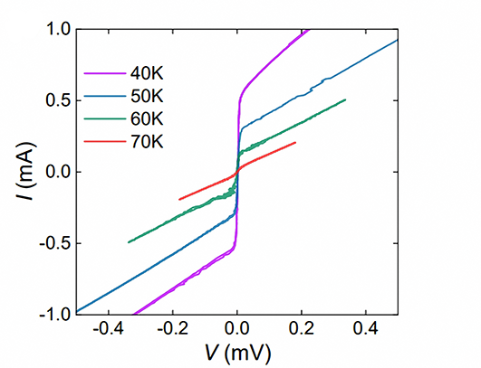
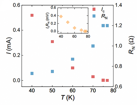
Figure 2 shows IV curves (a), critical current , normal resistance , and their product (characteristic voltage) (b) of the Josephson junctions written with a dose of , which are measured at different temperatures from to . At , the critical current value is about , while the normal resistance is about , that results in the characteristic voltage value . For this junction, the normal resistance first decreases but then increases with temperature decreasing, indicating a barrier property somehow between metal and insulator.
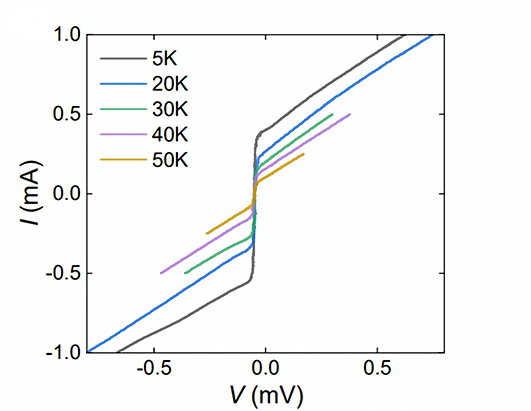
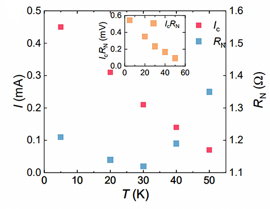
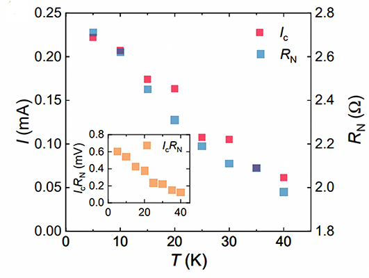
Further increasing the helium dose, Fig. 3 shows IV curves (a), critical current , normal resistance , and their product (characteristic voltage) (b) of the Josephson junctions fabricated using a dose of , which are measured at different temperatures from to . At , the critical current value is about , while the normal resistance is about , that results in the characteristic voltage value . For the junction written with a dose of , the normal resistance increases with temperature decreasing in contrast to the junctions written with a dose of . This fact indicates rather insulator-close type of the junction barrier. Hence, by simply controlling the helium dose parameter, the barrier characteristic can be regulated gradually, which benefits the following multi-junction device designing.
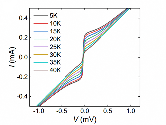
As one can see from Figs. 1 to 3, the fabricated HTS Josephson junctions show IV curves closed to the ones corresponding to the resistively shunted junction model (RSJ model) [2]of overdamped Josephson junctions (when the capacitive parameter, usually called as Stuart-McCumber parameter, , where is the junction capacitance) [2]. This is just the type of the junctions which are needed for designing a major part of the promising superconductor devises. Moreover, the obtained characteristic voltage values at are quite high and comparable with the ones of the resistively shunted Nb tunnel junctions.
III Discussion
Main advantages of the focused helium ion beam fabrication technique developed and reported here are: (i) the achievable high value of the characteristic voltage of the YBCO Josephson junctions; (ii) the controllable barrier characteristic; (iii) the ability to design a large number of arbitrary located Josephson junctions. These facts allow narrowing the existing gap in design abilities for LTS and HTS circuits even with using only single HTS film layer.
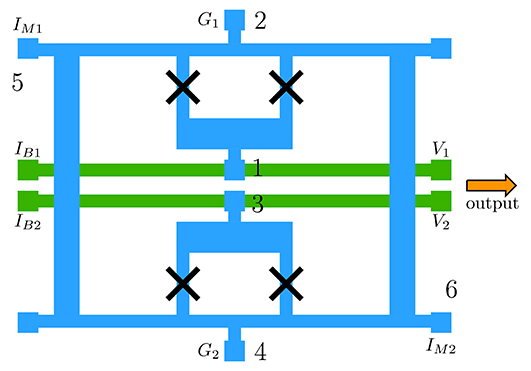
The attainable increase in the characteristic voltage of the used Josephson junctions essentially improves device performance (by increase in output voltage and signal frequency band) of all Josephson junction devices, including the simplest ones containing single dc SQUID or two dc SQUIDs. One of such highly promising devices is active broadband receiving electrically small antenna (ESA) based on using differential dc SQUID circuit (DSQUID) [45]. Figure 4 shows a schematic of the active ESA which can be formed on chip of very small size such as 5 by 5 mm2 or even less. The antenna contains quadratic superconducting strip loop and two dc SQUIDs with an independent dc current biasing in parallel. Two current sources each applying dc bias current are connected to points 1, 2 and 3, 4, respectively. A circular screening current is induced by an incident electromagnetic wave (namely, by a flux of its magnetic field component) in the superconducting loop, and therefore applies equal magnetic fluxes to both dc SQUIDs. An additional source of dc current is connected to points 5,6 to apply magnetic flux to each of the dc SQUIDs but with opposite signs to shift voltage responses of the dc SQUIDs in opposite directions. As far as a form of the voltage responses (at the critical current biasing is very close to parabolic law, difference of the voltage responses, which is an antenna output, measured between points 1,2 shows linear response to the incident wave. This linear response range allows peak-to-peak value of the signal magnetic flux, applied to the dc SQUIDs, up to about .
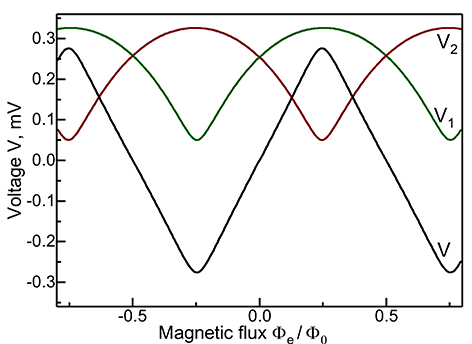
Figure 5 shows the voltage responses , of both dc SQUIDs and resulting voltage response of the antenna obtained by numerical simulation using PSCAN software [46, 47]. Maximum swing of the antenna voltage response can be as high as when normalized inductance of dc SQUIDs
| (2) |
is much less than (see [2, 3]) or about at as seen from Fig. 5. At a fixes size of dc SQUID loops and hence its inductance sensitivity of the ESA rises proportionally to linear size of the antenna loop. In fact, the signal magnetic flux applied to the dc SQUIDs is proportional to screening current induced in the antenna loop (where is the magnetic field component perpendicular to the antenna chip plane, is the antenna loop size, and is the antenna loop inductance) and this current rises proportionally to the size since is proportional to , while is proportional to .
Further development of the active electrically small antenna (ESA) can be obtained by replacing two dc SQUIDs by two parallel arrays of Josephson junctions, i.e. with realizing a particular case of active ESA based on SQA (superconducting quantum array) [30] composed of differential unit blocks [32]. Such a design approach can be used also to develop high-performance rf amplifiers.
The use of multi-junction array structures like SQAs [30] or SQIF [28, 29] enables an increase of overall device performance, including increase in dynamic range of the multi-junction devices, through increase in signal-to-noise ratio (SNR) with the number of unit cells proportional to . In fact, as long as intrinsic fluctuations in array cells are independent, spectral density of the low-frequency voltage fluctuations (at the signal frequency ) across the serially connected cells , where is the spectral density across one cell. Thus, the rms fluctuation voltage , where is the frequency band, increases as , whereas both the maximum output signal and transfer factor of the flux to voltage transformation increases as . Therefore, dynamic range increases as . In case of cells connected in parallel, both the maximum output voltage and transfer factor don’t change with , while the spectral density of the low frequency current fluctuations becomes times higher than the one for one cell , and therefore the rms fluctuation voltage , where is differential resistance at operation point on IV curve of one cell, decreases as , and hence dynamic range increases also as .
IV Conclusion
The obtained progress in the HTS (YBCO) Josephson junction fabrication process founded on using a focused helium ion beam damaging technique enables achieving characteristic voltage value up to about and potentially higher. Both the high value of of Josephson junctions and the ability to design a large number of arbitrary located Josephson junctions allow narrowing the existing gap in design abilities for LTS and HTS circuits even with using a single HTS film layer. A one-layer topology of active electrically small antenna is suggested and the antenna voltage response characteristics are considered. Such a design approach can be also used to develop high-performance rf amplifiers. Further development of the active devices can be obtained by using multi-junction array structures like SQAs which enables an increase in overall performance, including increase in dynamic range of the multi-junction devices, through increase of signal-to-noise ratio (SNR) with the number of unit cells proportional to .
Acknowledgements.
This work was supported by National Key R&D Program of China 2022YFA1603900 and in part by Russian Science Foundation (RSCF) grant, no. 19-72-10016-P.References
- Schmidt [1997] V. V. Schmidt, The Physics of Superconductors, edited by P. Müller and A. V. Ustinov (Springer Berlin Heidelberg, 1997).
- Likharev [1986] K. Likharev, Dynamics of Josephson Junctions and Circuits (Gordon and Breach Science Publishers, 1986).
- Seidel [2015] P. Seidel, ed., Applied Superconductivity, Encyclopedia of Applied Physics (Wiley-VCH Verlag GmbH & Co. KGaA, 2015).
- Mukhanov et al. [2004] O. Mukhanov, D. Gupta, A. Kadin, and V. Semenov, Superconductor analog-to-digital converters, Proceedings of the IEEE 92, 1564 (2004).
- Inamdar et al. [2009] A. Inamdar, S. Rylov, A. Talalaevskii, A. Sahu, S. Sarwana, D. Kirichenko, I. Vernik, T. Filippov, and D. Gupta, Progress in design of improved high dynamic range analog-to-digital converters, IEEE Transactions on Applied Superconductivity 19, 670 (2009).
- Vernik et al. [2007a] I. Vernik, D. Kirichenko, T. Filippov, A. Talalaevskii, A. Sahu, A. Inamdar, A. Kirichenko, D. Gupta, and O. Mukhanov, Superconducting high-resolution low-pass analog-to-digital converters, IEEE Transactions on Applied Superconductivity 17, 442 (2007a).
- Sarwana et al. [2009] S. Sarwana, D. Kirichenko, D. Gupta, and A. Kirichenko, Dual-band ADC utilizing switch matrix, IEEE Transactions on Applied Superconductivity 19, 661 (2009).
- Gupta et al. [2011a] D. Gupta, A. Inamdar, D. E. Kirichenko, A. M. Kadin, and O. A. Mukhanov, Superconductor analog-to-digital converters and their applications, in Microwave Symposium Digest (MTT), 2011 IEEE MTT-S International (IEEE, 2011) pp. 1–4.
- Herr et al. [2015] Q. P. Herr, J. Osborne, M. J. A. Stoutimore, H. Hearne, R. Selig, J. Vogel, E. Min, V. V. Talanov, and A. Y. Herr, Reproducible operating margins on a 72 800-device digital superconducting chip, Superconductor Science and Technology 28, 124003 (2015).
- Yamanashi et al. [2007] Y. Yamanashi, M. Tanaka, A. Akimoto, H. Park, Y. Kamiya, N. Irie, N. Yoshikawa, A. Fujimaki, H. Terai, and Y. Hashimoto, Design and implementation of a pipelined bit-serial sfq microprocessor, , IEEE Transactions on Applied Superconductivity 17, 474 (2007).
- Filippov et al. [2012] T. V. Filippov, A. Sahu, A. F. Kirichenko, I. V. Vernik, M. Dorojevets, C. L. Ayala, and O. A. Mukhanov, 20ghz operation of an asynchronous wave-pipelined rsfq arithmetic-logic unit, Physics Procedia 36, 59 (2012).
- Ando et al. [2016] Y. Ando, R. Sato, M. Tanaka, K. Takagi, N. Takagi, and A. Fujimaki, Design and demonstration of an 8-bit bit-serial RSFQ microprocessor: CORE e4, IEEE Transactions on Applied Superconductivity 26, 1 (2016).
- Filippov et al. [2024] T. V. Filippov, A. Sahu, D. E. Kirichenko, M. E. Çelik, and D. Gupta, Experimental evaluation of josephson balanced comparators toward 100 GHz RSFQ circuits, IEEE Transactions on Applied Superconductivity 34, 1 (2024).
- Mukhanov et al. [1987] O. Mukhanov, V. Semenov, and K. Likharev, Ultimate performance of the RSFQ logic circuits, IEEE Transactions on Magnetics 23, 759 (1987).
- Polonsky et al. [1993] S. Polonsky, V. Semenov, P. Bunyk, A. Kirichenko, A. Kidiyarov-Shevchenko, O. Mukhanov, P. Shevchenko, D. Schneider, D. Zinoviev, and K. Likharev, New RSFQ circuits (josephson junction digital devices), IEEE Transactions on Applied Superconductivity 3, 2566 (1993).
- Bunyk et al. [2001] P. Bunyk, K. Likharev, and D. Zinoviev, RSFQ technology: Physics and devices, International Journal of High Speed Electronics and Systems 11, 257 (2001).
- Mukhanov [2011] O. A. Mukhanov, Energy-efficient single flux quantum technology, IEEE Transactions on Applied Superconductivity 21, 760 (2011).
- Kirichenko et al. [2011] D. E. Kirichenko, S. Sarwana, and A. F. Kirichenko, Zero static power dissipation biasing of rsfq circuits, IEEE Transactions on Applied Superconductivity 21, 776 (2011).
- Volkmann et al. [2012] M. H. Volkmann, A. Sahu, C. J. Fourie, and O. A. Mukhanov, Implementation of energy efficient single flux quantum digital circuits with sub-aj/bit operation, Superconductor Science and Technology 26, 015002 (2012).
- Herr et al. [2011] Q. P. Herr, A. Y. Herr, O. T. Oberg, and A. G. Ioannidis, Ultra-low-power superconductor logic, Journal of Applied Physics 109, 103903 (2011).
- Takeuchi et al. [2013] N. Takeuchi, D. Ozawa, Y. Yamanashi, and N. Yoshikawa, An adiabatic quantum flux parametron as an ultra-low-power logic device, Superconductor Science and Technology 26, 035010 (2013).
- Holmes et al. [2013] D. S. Holmes, A. L. Ripple, and M. A. Manheimer, Energy-efficient superconducting computing – power budgets and requirements, IEEE Transactions on Applied Superconductivity 23, 1701610 (2013).
- Huber et al. [2001] M. E. Huber, P. A. Neil, R. G. Benson, D. A. Burns, A. F. Corey, C. S. Flynn, Y. Kitaygorodskaya, O. Massihzadeh, J. M. Martinis, and G. C. Hilton, Dc squid series array amplifiers with 120 mhz bandwidth, IEEE Transactions on Appiled Superconductivity 11, 4048 (2001).
- Macklin et al. [2015] C. Macklin, K. O’Brien, D. Hover, M. E. Schwartz, V. Bolkhovsky, X. Zhang, W. D. Oliver, and I. Siddiqi, A near–quantum-limited josephson traveling-wave parametric amplifier, Science 350, 307 (2015).
- White et al. [2015] T. C. White, J. Y. Mutus, I.-C. Hoi, R. Barends, B. Campbell, Y. Chen, Z. Chen, B. Chiaro, A. Dunsworth, E. Jeffrey, J. Kelly, A. Megrant, C. Neill, P. J. J. O’Malley, P. Roushan, D. Sank, A. Vainsencher, J. Wenner, S. Chaudhuri, J. Gao, and J. M. Martinis, Traveling wave parametric amplifier with josephson junctions using minimal resonator phase matching, Applied Physics Letters 106, 242601 (2015).
- Bell and Samolov [2015] M. Bell and A. Samolov, Traveling-wave parametric amplifier based on a chain of coupled asymmetric SQUIDs, Physical Review Applied 4, 024014 (2015).
- Zorin [2016] A. Zorin, Josephson traveling-wave parametric amplifier with three-wave mixing, Physical Review Applied 6, 034006 (2016).
- Caputo et al. [2005] P. Caputo, J. Tomes, J. Oppenlander, C. Haussler, A. Friesch, T. Trauble, and N. Schopohl, Superconducting quantum interference filters as absolute magnetic field sensors, IEEE Transactions on Appiled Superconductivity 15, 1044 (2005).
- Oppenländer et al. [2001] J. Oppenländer, T. Träuble, C. Häussler, and N. Schopohl, Superconducting multiple loop quantum interferometers, IEEE Transactions on Appiled Superconductivity 11, 1271 (2001).
- Kornev et al. [2014] V. K. Kornev, A. V. Sharafiev, I. I. Soloviev, N. V. Kolotinskiy, V. A. Scripka, and O. A. Mukhanov, Superconducting quantum arrays, IEEE Transactions on Applied Superconductivity 24, 1 (2014).
- Kornev et al. [2016] V. K. Kornev, A. V. Sharafiev, I. I. Soloviev, N. V. Kolotinskiy, and O. A. Mukhanov, A guide to active antennas based on superconducting quantum arrays, IEEE Transactions on Applied Superconductivity 26, 1 (2016).
- Kornev et al. [2017] V. K. Kornev, N. V. Kolotinskiy, A. V. Sharafiev, I. I. Soloviev, and O. A. Mukhanov, Broadband active electrically small superconductor antennas, Superconductor Science and Technology 30, 103001 (2017).
- Brock et al. [2001] D. Brock, O. Mukhanov, and J. Rosa, Superconductor digital RF development for software radio, IEEE Communications Magazine 39, 174 (2001).
- Gupta et al. [2002] D. Gupta, O. Mukhanov, A. Kadin, J. Rosa, and D. Nicholson, Benefits of superconductor digital-rf transceiver technology to future wireless systems, in Proc. SDR Technical Conference, Vol. I (2002) pp. 221–226.
- Vernik et al. [2007b] I. V. Vernik, D. E. Kirichenko, V. V. Dotsenko, R. Miller, R. J. Webber, P. Shevchenko, A. Talalaevskii, D. Gupta, and O. A. Mukhanov, Cryocooled wideband digital channelizing radio-frequency receiver based on low-pass ADC, Superconductor Science and Technology 20, S323 (2007b).
- Gupta et al. [2011b] D. Gupta, D. E. Kirichenko, V. V. Dotsenko, R. Miller, S. Sarwana, A. Talalaevskii, J. Delmas, R. J. Webber, S. Govorkov, A. F. Kirichenko, I. V. Vernik, and J. Tang, Modular, multi-function digital-rf receiver systems, IEEE Transactions on Applied Superconductivity 21, 883 (2011b).
- Sarwana et al. [2011] S. Sarwana, D. E. Kirichenko, V. V. Dotsenko, A. F. Kirichenko, S. B. Kaplan, and D. Gupta, Multi-band digital-rf receiver, IEEE Transactions on Applied Superconductivity 21, 677 (2011).
- [38] SEEQC: Chip foundry.
- Taylor et al. [2016] B. J. Taylor, S. A. E. Berggren, M. C. O’Brien, M. C. deAndrade, B. A. Higa, and A. M. L. d. Escobar, Characterization of large two-dimensional YBa2Cu3O7- SQUID arrays, Superconductor Science and Technology 29, 084003 (2016).
- Cho et al. [2015] E. Y. Cho, M. K. Ma, C. Huynh, K. Pratt, D. N. Paulson, V. N. Glyantsev, R. C. Dynes, and S. A. Cybart, YBa2Cu3O7- superconducting quantum interference devices with metallic to insulating barriers written with a focused helium ion beam, Applied Physics Letters 106, 252601 (2015).
- Ouanani et al. [2016] S. Ouanani, J. Kermorvant, C. Ulysse, M. Malnou, Y. Lemaître, B. Marcilhac, C. Feuillet-Palma, N. Bergeal, D. Crété, and J. Lesueur, High-Tc superconducting quantum interference filters (SQIFs) made by ion irradiation, Superconductor Science and Technology 29, 094002 (2016).
- Pawlowski et al. [2018] E. R. Pawlowski, J. Kermorvant, D. Crété, Y. Lemaître, B. Marcilhac, C. Ulysse, F. Couëdo, C. Feuillet-Palma, N. Bergeal, and J. Lesueur, Static and radio frequency magnetic response of high Tc superconducting quantum interference filters made by ion irradiation, Superconductor Science and Technology 31, 095005 (2018).
- Couëdo et al. [2019] F. Couëdo, E. R. Pawlowski, J. Kermorvant, J. Trastoy, D. Crété, Y. Lemaître, B. Marcilhac, C. Ulysse, C. Feuillet-Palma, N. Bergeal, and J. Lesueur, High-Tc superconducting detector for highly-sensitive microwave magnetometry, Applied Physics Letters 114, 192602 (2019).
- Xiong et al. [2023] P.-Y. Xiong, F.-C. Chen, Z.-P. Feng, J.-T. Yang, Y.-D. Xia, Y.-F. Yuan, X. Wang, J. Yuan, Y. Wu, J. Shi, and K. Jin, Optimization of large-area YBa2Cu3O7- thin films by pulsed laser deposition for planar microwave devices, Chinese Physics B 32, 077402 (2023).
- Soloviev et al. [2019] I. I. Soloviev, V. I. Ruzhickiy, N. V. Klenov, S. V. Bakurskiy, and M. Y. Kupriyanov, A linear magnetic flux-to-voltage transfer function of a differential DC SQUID, Superconductor Science and Technology 32, 074005 (2019).
- Polonsky et al. [1991] S. V. Polonsky, V. K. Semenov, and P. N. Shevchenko, PSCAN: personal superconductor circuit analyser, Superconductor Science and Technology 4, 667 (1991).
- Polonsky et al. [1997] S. Polonsky, P. Shevchenko, A. Kirichenko, D. Zinoviev, and A. Rylyakov, PSCAN'96: new software for simulation and optimization of complex RSFQ circuits, IEEE Transactions on Appiled Superconductivity 7, 2685 (1997).