Microwave dependent quantum transport characteristics in GaN/AlGaN FETs
Abstract
Defects in semiconductors, traditionally seen as detrimental to electronic device performance, have emerged as potential assets in quantum technologies due to their unique quantum properties. This study investigates the interaction between defects and quantum electron transport in GaN/AlGaN field-effect transistors, highlighting the observation of Fano resonances at low temperatures. We observe the resonance spectra and their dependence on gate voltage and magnetic fields. To explain the observed behavior, we construct the possible scenario as a Fano interferometer with finite width. Our findings reveal the potential of semiconductor defects to contribute to the development of quantum information processing, providing their role to key components in next-generation quantum devices.
In electronics applications, defects in solid states are typically viewed as detrimental, impacting device quality, integrated circuit yield, and electrical noise [1]. Conversely, from a quantum mechanical perspective, the isolated energy levels introduced by these defects have garnered significant interest [2]. Many studies have explored the unique properties of defects for their potential applications in advanced optics [3] and quantum computation [4, 5, 6, 7]. These isolated energy levels can act as quantum bits (qubits) for information processing, a high-sensitive magnetic sensor, and emissive centers in quantum optics, offering a pathway to exploit defects for innovative technologies [8].
Quantum transport phenomena in solid states, such as quantum Hall effect, single-electron transport, and Josephson tunneling are quite important for quantum devices, which are based on quantum mechanics and are expected to beyond conventional electronic devices [9, 10, 11, 12, 13]. Among them, those observed in semiconductor nano-structures are attractive from the viewpoint of compatibility with semiconductor manufacturing technologies [14, 15, 16]. We can design the various nano-structures using the technologies and control properties of the quantum transport phenomena in those. Quantum dots [17, 18, 19, 20, 21, 22] are one of the prospective structures for the realization of quantum computation [23].
Exploring the interaction between defects and quantum electron transport in semiconductor devices presents a fascinating research avenue. This interplay is crucial for understanding how defects influence quantum behavior in semiconductors, potentially providing interesting functionalities in quantum sensing and information processing technologies. By investigating these interactions, we can not only gain deeper insights into fundamental physics but also improve the design and performance of semiconductor devices. Experiments previously reported [24, 25, 26, 27] have turned the spotlight on defects or trapped states at the silicon-based semiconductor/oxide interface, traditionally considered a source of electrical noise in field-effect transistors (FETs). Moreover, relatively long coherence times of 1 to 40 have been demonstrated by controlling the defects as a quantum two-level system [27]. These findings underscore the potential of such defects not merely as nuisances but as gateways to new qubits and physical insights in semiconductor devices.
In this study, we investigate the microwave-dependent quantum transport in the low-temperature conduction of GaN/AlGaN FETs [28, 29, 30, 31]. Previously, we observed the formation of quantum dots in GaN/AlGaN FETs, near the pinch-off condition at a cryogenic temperature [32, 33, 34]. The possible mechanism is the disturbed potential caused by impurities and defects near the conduction channel of the FETs. Because the transport is modified by the states of the impurities and defects, it can be able to observe resonance spectra by applying microwaves, as in previous studies [24, 25, 26, 27]. We also measure the gate voltage and in-plane magnetic field dependence of the microwave resonance to discuss the possible current path.
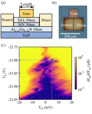
Figure 1(a) presents a diagram of the device’s layered structure. Layers of GaN and AlGaN are deposited on a silicon substrate through chemical vapor deposition. A two-dimensional electron gas forms at the GaN and AlGaN interface, exhibiting typical electron densities and mobilities of and , respectively. Titanium and aluminum are employed for the source and drain contacts. The gate insulators are made of SiN and , with a TiN gate electrode layered above. The FET has gate dimensions of 0.6 in length and 150 in width. The optical image of the device is shown in Fig. 1(b). The source-drain current is measured as a function of the source-drain voltage and the gate voltage . A microwave from a signal generator is applied to the gate electrode through a homemade cryogenic bias tee. To measure the electron transport properties at low temperatures of 2.3 K, we use a helium depressurization refrigerator.
Figure 1(c) shows a typical electron transport characteristics near the pinch-off state of the FET at 2.3 K. The differential conductance are measured as a function of and . We observed overlapped Coulomb diamond structures because of the formation of multiple quantum dots in the conduction channel. This is due to the potential fluctuations by impurities or defects near the conduction channel [32, 33]. The blue point in Fig. 1(c) shows the typical measurement point for the microwave resonance measurement. We set and at this point and measure with sweeping microwave frequency.
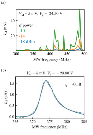
Figure 2(a) presents a typical result of the microwave resonance experiments and its power dependence. When sweeping the microwave frequency, the is modulated, revealing several resonance spectra. The observed resonance is attributed to opening defect levels as current paths upon the application of microwaves. This phenomenon aligns with findings from previous studies [27] and is identified as a Fano resonance. Fano resonance is characterized by a unique interference effect between a discrete quantum state and a continuum, leading to an asymmetric line shape in the resonance spectra [35]. The line shape of the resonance spectra remains unchanged across different microwave power levels. Notably, the resonance spectra exhibit a linewidth within the range of 1-10 MHz. In contrast, a previous study involving Si FETs reported a linewidth of approximately 60 kHz [26, 27]. The observed broader linewidths in our study may be attributed to the shorter lifetimes and broadening of the discrete energy levels contributing to resonance in GaN FETs. Note that these resonance peaks are reproducible during the sample is maintained at low temperatures. We also perform the measurements after subjecting the sample to thermal cycling and light exposure. These processes altered the detailed structures of the resonance peaks, although the overall frequency range of the peaks remained consistent. The observed changes are likely due to the redistribution of charged impurities and defects induced by thermal and optical cycles. These resonance spectra are not observed in the pinch-off state (). Additionally, we measure the transmission coefficient of the high-frequency circuit line using a network analyzer and confirm that there are no reflection peaks corresponding to the frequency at which the resonance spectra are observed.
Here, we focus on the resonance spectra around 375 MHz as shown in Fig. 2(b). This resonance spectra with the Fano-like line shape are described by the Fano formula [35, 36, 37, 38, 27]:
| (1) |
where is the transmission probability and the normalized energy expressed by . and are the resonance frequency and the linewidth, respectively. is the Fano parameter representing the resonance peak’s asymmetry. The results of the fitting using this equation with a free parameter are shown in Fig. 2(b), and well reproduced the experimental data.
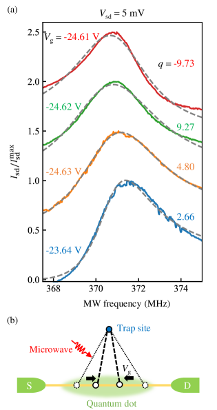
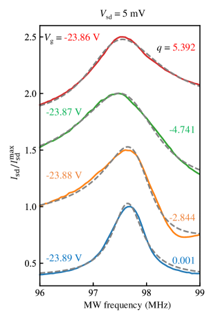
Fig. 3(a) shows the dependence of the microwave resonance spectrum. In this measurement, is also fixed at 5 mV, and is measured at four points between -23.64 V and -24.61 V in 0.01 V increments. For comparison, the measurement results were normalized to the maximum value of the resonance spectrum, , and an offset is added. At a glance, the shape of the resonance spectrum is modulated by the change of . We fit the spectrum by using Eq. 1, and the extracted parameters are shown in Fig. 3(a). The value and sign of , which represents the asymmetry of the peak, changes by changing the . There is another resonance spectrum around 97.5 MHz obtaining similar dependence, which is detailed in Appendix A.
To explain the change of the line shape by the change of , we construct a possible model. It is a Fano interferometer with finite width as shown in Fig. 3(b) [38]. The trapping sites in the FET, caused by impurities or defects, exhibit an energy level distribution influenced by temperature and/or carrier lifetime. The width of the Coulomb peak also indicates the energy level distribution within the system, primarily determined by the tunneling rate between the quantum dots and the electrodes. In GaN/AlGaN quantum dots, the typical energy distribution spans a few millielectronvolts [33], a range that is considerably broader than the linewidth observed in the Fano resonance spectrum. This suggests that the trapping sites within our device act as effective discrete states, influencing the microwave resonance. The trapping site couples to the current path with finite width: several points in the current path coupled to the trapping site. With the change of , some parameters of the system, such as coupling between continuous and discrete paths, are modified. This induces the change in the interference and we observe the change of the Fano resonance spectrum. We perform a tight-binding calculation to support our scenario in Appendix B.
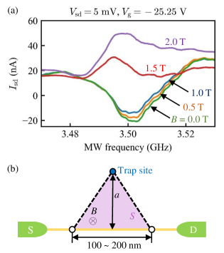
Several resonance spectra show a change in the line shape by applying the in-plane magnetic field to the two-dimensional electron gas, as shown in Fig. 4. In this measurement, the bias was fixed at and . The in-plane magnetic field changes from 0 T to 2 T in 0.5 T steps. Around 1.5 T, a steep change in the shape of the resonance spectrum is observed. A similar trend was observed in the reverse magnetic field direction. As to the possible mechanism, the additional phase induced by the magnetic field between the interference paths can be expected [36, 37]. Note that the negative current is observed in some cases, and the abrupt change occurs around 1.5 T. Only an additional phase cannot explain these behaviors. One of the possible scenarios of additional mechanisms is the photon-assisted back currents [39].
For the discussion, it is assumed that the abrupt change observed around 1.5 T is due to phase inversion, with a magnetic flux quantum entering the triangular region depicted in Figure 4(b). Taking into account that the coupling width ranges from 100 to 200 nm, which corresponds to the potential fluctuation in the conduction channel as mentioned in previous work [33], we estimate the distance between the current path and the trapping site to be nm from the . This value aligns with the geometry of our device, supporting the hypothesis that the resonance spectrum is induced by defects or impurities near the conduction channel [40]. Furthermore, there is no response on the resonance spectrum when the magnetic field is applied in the 2DEG normal direction, which indicates that the area pierced by magnetic flux is not formed in the 2DEG plane.
In conclusion, we measure electron transport under microwave irradiation at low-temperature in GaN/AlGaN FETs. Asymmetric resonance spectra are observed near the pinch-off of the FET channel, where the quantum dots form. The shape of some peaks is modified by the gate voltage and the in-plane magnetic field. These behaviors are explained by the Fano interferometer. From this model, we estimate that the Fano resonances are induced due to interaction between the conduction channel and defect sites in AlGaN or insulating layers. Our findings open avenues for employing GaN/AlGaN FETs in quantum devices, offering potential applications in defect-based qubit manipulation and evaluating defects in semiconductor devices.
I Acknowledgements
The authors thank N, Ito, T, Tanaka, K, Nakahara, Y. Tokura, RIEC Fundamental Technology Center and the Laboratory for Nanoelectronics and Spintronics for fruitful discussions and technical supports. Part of this work is supported by Rohm Collaboration Project, MEXT Leading Initiative for Excellent Young Researchers, Grants-in-Aid for Scientific Research (21K18592, 23H01789, 23H04490), Hattori Hokokai Foudation Research Grant, The Foundation for Technology Promotion of Electronic Circuit Board, Iketani Science and Technology Foundation Research Grant, and FRiD Tohoku University.
II Appendix A: Gate voltage dependence of the resonance spectrum
Here, we present another resonance spectrum influenced by the gate voltage in Fig. 5. This behavior is similar to that we observed with the resonance spectrum approximately at 371 MHz, as illustrated in Fig. 3.
III Appendix B: Tight binding calculation
We perform a tight binding calculation to support our Fano effect model. We assume a one-dimensional model considering dots site energy and nearest neighbor hopping, where one trap site is coupled as shown in Figs. 6 (a) and (b). Here, , , , , , and are the channel dots energy, the trap site energy, and hopping parameters, respectively. The retarded Green’s function is described as
| (2) |
where , , , and are the Fermi energy of left and right lead electrodes, the identity matrix, the Hamiltonian of the conductor, and the self-energy of our model, respectively. From the Meir-Wingrenn fomula [41], the transmission probability can be derived as
| (3) |
| (4) |
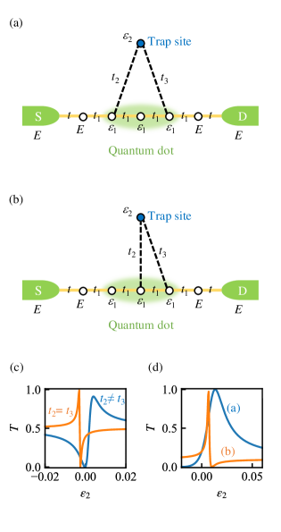
Here, we calculate the transmission probability by Eq. 3 under two models as shown in Figs. 6(a) and (b). Figure 6(c) presents a comparison between conditions and in the model of Fig. 6(a). We also present the results obtained by varying the coupling site under the condition in Fig. 6(d), corresponding to the models depicted in Figs. 6(a) and (b). Clearly, the sign of the Fano parameter, resonance frequency (energy), and linewidth are changing. The changes observed in the spectrum during the experiments may be attributed to the modulation of these and other potential parameters, such as , by the gate voltage.
References
- Chang et al. [1994] J. Chang, A. Abidi, and C. Viswanathan, Flicker noise in cmos transistors from subthreshold to strong inversion at various temperatures, IEEE Trans. Electron Devices 41, 1965 (1994).
- Wolfowicz et al. [2021] G. Wolfowicz, F. J. Heremans, C. P. Anderson, S. Kanai, H. Seo, A. Gali, G. Galli, and D. D. Awschalom, Quantum guidelines for solid-state spin defects, Nat. Rev. Mater. 6, 906 (2021).
- Aharonovich et al. [2011] I. Aharonovich, S. Castelletto, D. Simpson, C.-H. Su, A. Greentree, and S. Prawer, Diamond-based single-photon emitters, Rep. Prog. Phys. 74, 076501 (2011).
- Weber et al. [2010] J. Weber, W. Koehl, J. Varley, A. Janotti, B. Buckley, C. Van de Walle, and D. D. Awschalom, Quantum computing with defects, Proc. Natl. Acad. Sci. U.S.A. 107, 8513 (2010).
- Koehl et al. [2011] W. F. Koehl, B. B. Buckley, F. J. Heremans, G. Calusine, and D. D. Awschalom, Room temperature coherent control of defect spin qubits in silicon carbide, Nature 479, 84 (2011).
- Wolfowicz et al. [2013] G. Wolfowicz, A. M. Tyryshkin, R. E. George, H. Riemann, N. V. Abrosimov, P. Becker, H.-J. Pohl, M. L. Thewalt, S. A. Lyon, and J. J. Morton, Atomic clock transitions in silicon-based spin qubits, Nat. Nanotechnol. 8, 561 (2013).
- Widmann et al. [2015] M. Widmann, S.-Y. Lee, T. Rendler, N. T. Son, H. Fedder, S. Paik, L.-P. Yang, N. Zhao, S. Yang, I. Booker, et al., Coherent control of single spins in silicon carbide at room temperature, Nat. Mater. 14, 164 (2015).
- Anderson et al. [2019] C. P. Anderson, A. Bourassa, K. C. Miao, G. Wolfowicz, P. J. Mintun, A. L. Crook, H. Abe, J. Ul Hassan, N. T. Son, T. Ohshima, et al., Electrical and optical control of single spins integrated in scalable semiconductor devices, Science 366, 1225 (2019).
- Klitzing et al. [1980] K. v. Klitzing, G. Dorda, and M. Pepper, New method for high-accuracy determination of the fine-structure constant based on quantized hall resistance, Phys. Rev. Lett. 45, 494 (1980).
- Jeckelmann and Jeanneret [2003] B. Jeckelmann and B. Jeanneret, The quantum hall effect as an electrical resistance standard, Meas. Sci. Technol. 14, 1229 (2003).
- Kastner [1992] M. A. Kastner, The single-electron transistor, Rev. Mod. Phys. 64, 849 (1992).
- Chen et al. [1996] R. Chen, A. Korotkov, and K. Likharev, Single-electron transistor logic, Appl. Phys. Lett. 68, 1954 (1996).
- Makhlin et al. [2001] Y. Makhlin, G. Schön, and A. Shnirman, Quantum-state engineering with josephson-junction devices, Rev. Mod. Phys. 73, 357 (2001).
- Tarucha et al. [1996] S. Tarucha, D. G. Austing, T. Honda, R. J. van der Hage, and L. P. Kouwenhoven, Shell filling and spin effects in a few electron quantum dot, Phys. Rev. Lett. 77, 3613 (1996).
- Hanson et al. [2007] R. Hanson, L. P. Kouwenhoven, J. R. Petta, S. Tarucha, and L. M. Vandersypen, Spins in few-electron quantum dots, Rev. Mod. Phys. 79, 1217 (2007).
- Li et al. [2006] Y. Li, F. Qian, J. Xiang, and C. M. Lieber, Nanowire electronic and optoelectronic devices, Mater. Today 9, 18 (2006).
- Gaudreau et al. [2006] L. Gaudreau, S. A. Studenikin, A. S. Sachrajda, P. Zawadzki, A. Kam, J. Lapointe, M. Korkusinski, and P. Hawrylak, Stability diagram of a few-electron triple dot, Phys. Rev. Lett. 97, 036807 (2006).
- Braakman et al. [2013] F. R. Braakman, P. Barthelemy, C. Reichl, W. Wegscheider, and L. M. Vandersypen, Long-distance coherent coupling in a quantum dot array, Nat. Nanotechnol. 8, 432 (2013).
- Takakura et al. [2014] T. Takakura, A. Noiri, T. Obata, T. Otsuka, J. Yoneda, K. Yoshida, and S. Tarucha, Single to quadruple quantum dots with tunable tunnel couplings, Appl. Phys. Lett. 104 (2014).
- Ito et al. [2016] T. Ito, T. Otsuka, S. Amaha, M. R. Delbecq, T. Nakajima, J. Yoneda, K. Takeda, G. Allison, A. Noiri, K. Kawasaki, et al., Detection and control of charge states in a quintuple quantum dot, Sci. Rep. 6, 39113 (2016).
- Ito et al. [2018] T. Ito, T. Otsuka, T. Nakajima, M. R. Delbecq, S. Amaha, J. Yoneda, K. Takeda, A. Noiri, G. Allison, A. Ludwig, et al., Four single-spin rabi oscillations in a quadruple quantum dot, Appl. Phys. Lett. 113 (2018).
- Noiri et al. [2018] A. Noiri, T. Nakajima, J. Yoneda, M. Delbecq, P. Stano, T. Otsuka, K. Takeda, S. Amaha, G. Allison, K. Kawasaki, et al., A fast quantum interface between different spin qubit encodings, Nat. Commun. 9, 5066 (2018).
- Loss and DiVincenzo [1998] D. Loss and D. P. DiVincenzo, Quantum computation with quantum dots, Phys. Rev. A 57, 120 (1998).
- Ferrus et al. [2009] T. Ferrus, D. Hasko, Q. Morrissey, S. Burge, E. Freeman, M. French, A. Lam, L. Creswell, R. Collier, D. Williams, et al., Cryogenic instrumentation for fast current measurement in a silicon single electron transistor, J. Appl. Phys. 106 (2009).
- Rossi and Hasko [2010] A. Rossi and D. Hasko, Microwave-assisted transport via localized states in degenerately doped si single electron transistors, J. Appl. Phys. 108 (2010).
- Erfani et al. [2011] M. Erfani, D. G. Hasko, A. Rossi, W. Sik Cho, and J.-B. Choi, Microwave driven arbitrary coupling between trapped charge resonances in a silicon single electron transistor, Appl. Phys. Lett. 99 (2011).
- Tenorio-Pearl et al. [2017] J. Tenorio-Pearl, E. Herbschleb, S. Fleming, C. Creatore, S. Oda, W. Milne, and A. Chin, Observation and coherent control of interface-induced electronic resonances in a field-effect transistor, Nat. Mater. 16, 208 (2017).
- Ambacher et al. [1999] O. Ambacher, J. Smart, J. Shealy, N. Weimann, K. Chu, M. Murphy, W. Schaff, L. Eastman, R. Dimitrov, L. Wittmer, et al., Two-dimensional electron gases induced by spontaneous and piezoelectric polarization charges in N-and Ga-face AlGaN/GaN heterostructures, J. Appl. Phys. 85, 3222 (1999).
- Manfra et al. [2004] M. Manfra, K. Baldwin, A. Sergent, K. West, R. Molnar, and J. Caissie, Electron mobility exceeding 160000 cm2/Vs in AlGaN/GaN heterostructures grown by molecular-beam epitaxy, Appl. Phys. Lett. 85, 5394 (2004).
- Thillosen et al. [2006] N. Thillosen, S. Cabanas, N. Kaluza, V. Guzenko, H. Hardtdegen, and T. Schäpers, Weak antilocalization in gate-controlled AlxGa1-xN/GaN two-dimensional electron gases, Phys. Rev. B 73, 241311 (2006).
- Shchepetilnikov et al. [2018] A. Shchepetilnikov, D. Frolov, V. Solovyev, Y. A. Nefyodov, A. Großer, T. Mikolajick, S. Schmult, and I. Kukushkin, Electron spin resonance in a 2d system at a GaN/AlGaN heterojunction, Appl. Phys. Lett. 113, 052102 (2018).
- Otsuka et al. [2020] T. Otsuka, T. Abe, T. Kitada, N. Ito, T. Tanaka, and K. Nakahara, Formation of quantum dots in GaN/AlGaN FETs, Sci. Rep. 10, 15421 (2020).
- Matsumura et al. [2023] K. Matsumura, T. Abe, T. Kitada, T. Kumasaka, N. Ito, T. Tanaka, K. Nakahara, and T. Otsuka, Channel length dependence of the formation of quantum dots in GaN/AlGaN FETs, Appl. Phys. Express 16, 075003 (2023).
- Fujiwara et al. [2023] Y. Fujiwara, M. Shinozaki, K. Matsumura, K. Noro, R. Tataka, S. Sato, T. Kumasaka, and T. Otsuka, Wide dynamic range charge sensor operation by high-speed feedback control of radio-frequency reflectometry, Appl. Phys. Lett. 123 (2023).
- Fano [1961] U. Fano, Effects of configuration interaction on intensities and phase shifts, Phys. Rev. 124, 1866 (1961).
- Kobayashi et al. [2002] K. Kobayashi, H. Aikawa, S. Katsumoto, and Y. Iye, Tuning of the fano effect through a quantum dot in an aharonov-bohm interferometer, Phys. Rev. Lett. 88, 256806 (2002).
- Kobayashi et al. [2003] K. Kobayashi, H. Aikawa, S. Katsumoto, and Y. Iye, Mesoscopic fano effect in a quantum dot embedded in an aharonov-bohm ring, Phys. Rev. B 68, 235304 (2003).
- Otsuka et al. [2007] T. Otsuka, E. Abe, S. Katsumoto, Y. Iye, G. L. Khym, and K. Kang, Fano effect in a few-electron quantum dot, J. Phys. Soc. Japan 76, 084706 (2007).
- Kouwenhoven et al. [1994] L. Kouwenhoven, S. Jauhar, J. Orenstein, P. McEuen, Y. Nagamune, J. Motohisa, and H. Sakaki, Observation of photon-assisted tunneling through a quantum dot, Phys. Rev. Lett. 73, 3443 (1994).
- Guerra et al. [2010] D. Guerra, M. Saraniti, N. Faralli, D. K. Ferry, S. M. Goodnick, and F. A. Marino, Comparison of N-and Ga-face GaN HEMTs through cellular Monte Carlo simulations, IEEE Trans. Electron Devices 57, 3348 (2010).
- Meir and Wingreen [1992] Y. Meir and N. S. Wingreen, Landauer formula for the current through an interacting electron region, Phys. Rev. Lett. 68, 2512 (1992).