Forward lateral photovoltage scanning problem: Perturbation approach and existence-uniqueness analysis
Abstract
In this paper, we present analytical results for the so-called forward lateral photovoltage scanning (LPS) problem. The (inverse) LPS model predicts doping variations in crystal by measuring the current leaving the crystal generated by a laser at various positions. The forward model consists of a set of nonlinear elliptic equations coupled with a measuring device modeled by a resistance. Standard methods to ensure the existence and uniqueness of the forward model cannot be used in a straightforward manner due to the presence of an additional generation term modeling the effect of the laser on the crystal. Hence, we scale the original forward LPS problem and employ a perturbation approach to derive the leading order system and the correction up to the second order in an appropriate small parameter. While these simplifications pose no issues from a physical standpoint, they enable us to demonstrate the analytic existence and uniqueness of solutions for the simplified system using standard arguments from elliptic theory adapted to the coupling with the measuring device.
Keywords: Drift-diffusion model, Charge transport, Lateral photovoltage scanning method (LPS), Perturbation analysis, Existence and uniqueness.
1 Introduction
Estimating crystal inhomogeneities in semiconductors noninvasively holds significance for various industrial applications. For example, understanding and avoiding doping fluctuations is important if very pure semiconductor crystal are required in industrial applications [23]. However, such fluctuations, often referred to as striations, may not always have a negative impact which may be the case for grain boundaries in solar cells [21].
Doping variations lead to local electrical fields. In order to detect inhomogeneities, variations, and defects in the doping profile noninvasively, one may systematically generate electron-hole pairs through some form of electromagnetic radiation and attach an external circuit to measure the resulting current. Due to the local fields created by doping inhomogeneities, charge carriers tend to redistribute in the surrounding region of the excitation to minimize energy. The excess charge carriers then traverse the external circuit, generating a measurable current. Scanning the semiconductor sample with the electromagnetic source at different positions allows one to visualize the distribution of electrically active charge-separating defects and variations in the doping profile along the scan locations. Several different types of technologies rely on this physical principle such as Electron Beam Induced Current (EBIC) [22], Laser Beam Induced Current (LBIC) [4], scanning photovoltage (SPV) [10], and Lateral Photovoltage Scanning (LPS) [15, 11, 12, 16]. While EBIC uses localized electron beams as the source of electromagnetic radiation, LBIC, SPV and LPS use laser beams.
In this paper, we focus on the LPS method. A nonlinear drift-diffusion model for the forward problem was mathematically formulated in [7], where the coupling between the charge transport in the crystal and the external circuit for the voltmeter is realized through an implicit boundary condition. This forward model computes current/voltages at the contacts for given doping variations. However, no analytical existence results were presented. The main difficulty in establishing the existence is due to the generation rate on the right-hand side of the continuity equations which impedes the direct use of standard arguments [3, 17]. Known existence results in the literature for related PDE models require the generation term to be small [5]. However, the authors in [7] demonstrated through simulations based on the Voronoi finite-volume method [9, 18, 8, 14, 1] that, on the one hand, numerically the system also converges for higher laser powers and that, on the other hand, the electron density is several orders of magnitude larger than the hole density. In this paper, we make use of the second fact by deriving an appropriately scaled unipolar model and identifying the relevant dimensionless small parameters. However, setting the smallest parameter to zero, oversimplifies the physics in the sense that the coupling between the circuit and the charge transport model is ignored. Therefore, through a perturbation approach the leading order corrections up to the second order in the small parameter are derived. The resulting system is simpler than the original LPS model. However, for realistic applications, for example studied in [7, 15, 11], these simplifications are reasonable since the perturbation parameters for silicon and gallium arsenide are small. Thus, these simplifications are not problematic from a physical point of view. Moreover, from a mathematical point of view, we have the additional benefit that the leading order model is a decoupled nonlinear elliptic system and the second order correction is a linear elliptic system coupled with the external circuit. The existence and uniqueness of solutions for the simplified model can be shown by using arguments from elliptic PDE theory modified to include the coupling with the external circuit. While this paper focuses on the mathematical analysis of the forward problem, it is worth noting that numerical, data-driven strategies exist to address the more complicated inverse problem [19], that is, the prediction of the doping variations in a crystal by measuring the current generated by a laser beam impinging at various positions of the crystal.
The remainder of this paper is organized as follows: In Section 2, we state the original LPS model. The model is then scaled in Section 3 and the asymptotic simplified model is derived in Section 4. In Section 5, we show the existence and uniqueness of solutions for the asymptotic PDE system and draw some conclusions in Section 6.
2 Lateral Photovoltage Scanning method
In this section, we present the model for the LPS method. The description of the model strongly relies on [7].
2.1 Presentation of the model
We represent the silicon crystal as a confined domain , where . The doping profile, denoted by for , reflects the difference between donor and acceptor concentrations.
Within the crystal, two charge carriers exist: electrons with a negative elementary charge and holes with a positive elementary charge . Charge transport is described by the electrostatic potential and quasi Fermi potentials and for electrons and holes, respectively, which are governed by the steady-state van Roosbroeck model:
| (1) |
The first equation describes a self-consistent electric field through a nonlinear Poisson equation. The subsequent continuity equations describe charge transport in the crystal, with constant permittivity and mobilities and . Assuming Boltzmann statistics, the relations between electron and hole densities and , and the quasi-Fermi potentials, are established by:
| (2) |
The effective conduction and valence band densities of states are denoted by and , while the Boltzmann constant and temperature are represented by and . The constant conduction and valence band-edge energies are denoted as and .
The current densities for electrons and holes, and , are expressed as and , respectively. Utilizing the relations (2), their drift-diffusion form is
| (3) |
where is the thermal voltage.
Recombination and generation rates are elaborated in subsequent sections.
The system (1) is complemented by mixed boundary conditions. The boundary comprises two disjoint parts, and . Neumann boundary conditions on are given by
| (4) |
where is the normal derivative along the external unit normal . On , Dirichlet-type boundary conditions model ohmic contacts
| (5) |
where is the local electroneutral potential (see [17] for details),
| (6) |
The parameter refers to the intrinsic carrier density defined by
| (7) |
The terms represent contact voltages at the respective ohmic contacts, with a common practice of defining a reference potential . The total electric current flowing through the -th ohmic contact is defined by the surface integral
| (8) |
Following charge conservation, the currents in (8) satisfy:
| (9) |
The voltage meter is simplified as a circuit with resistance , depicted in Figure 1. The potential difference between nodes and appearing in (5), is given by
| (10) |
where is defined in (9). By assuming that one node of an electric circuit is grounded, we can freely assign , resulting in the simplification of (10) to:
| (11) |
Equation (11) is an implicit equation for , given that depends implicitly on via the van Roosbroeck system (1). After obtaining a solution to the van Roosbroeck system, where influences the Dirichlet boundary condition (5), we compute the current using (8). Further insights into this coupling can be found in [2] and [3]. To simplify the notation, we will use instead of .
The total recombination rate, denoted as , includes three mechanisms:
| (12) |
where , , and represent direct recombination, Auger recombination, and Shockley-Read-Hall (SRH) recombination, respectively, defined as:
| (13) |
where , and are material-related constants. The SRH recombination process, which involves the trapping and release of charge carriers in semiconductors, differs from the Auger recombination process due to unintentional inclusion of elements during fabrication. This unintentional inclusion affects the properties of the semiconductor material, such as the lifetimes of charge carriers ( for electrons, for holes) and the reference densities of charge carriers ( for electrons, for holes). For later use we define the function
| (14) |
so that .
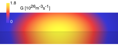
The electromagnetic source is modeled by the generation term . When the laser hits the crystal at the point , some photons are impinged and create electron-hole pairs, resulting in a generation rate defined as follows
| (15) |
where is the shape function of the laser (normalized by ), while is a constant given by , where is the velocity of light in vacuum. Here, is the laser power, is the wave length of the laser, is the Planck constant, and is the reflectivity rate of the crystal.
We assume that area of influence of the electromagnetic source decays exponentially fast from the incident point . In particular, we take a laser profile function defined as
| (16) |
Here is the laser spot radius, while is the penetration depth (or the reciprocal of the absorption coefficient), which heavily depends on the laser wave length.
2.2 Numerical simulations
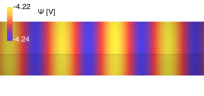
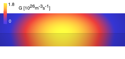
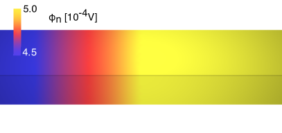
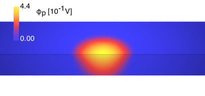
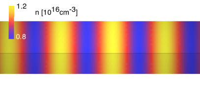
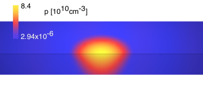
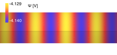
For the above model, we performed numerical simulation with ddfermi [6] of a donor-doped semiconductor crystal irradiated by a laser beam, both for silicon (see Figure 2) and gallium arsenide (see Figure 3). We set the laser power , laser spot position , average doping concentration and . The additional parameters for both simulations can be found in A. The results show that the presence of the beam, modeled by the generation term , greatly affects the minority charge carriers , while the majority charge carriers are not significantly impacted. As a matter of fact, the sinusoidal pattern of the doping is reflected in the electron densitiy and the electrostatic potential alone.
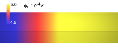
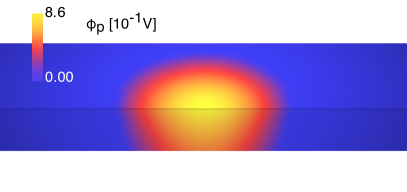
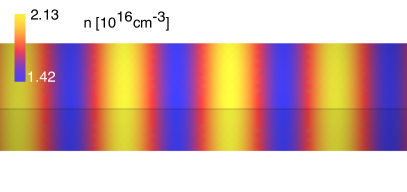
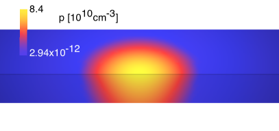
These numerical findings are the main motivation for a unipolar scaling of the full model, also encompassing the electric network variables, which will be detailed in the following section.
3 Scaling of the model for unipolar devices
We consider a scaling of the model (1) which is suitable for unipolar devices. In this case, the density of the majority charge carriers is of the same order as the doping profile, while the density of the minority charge carriers is much smaller. Nevertheless, both charge carriers contribute to the total current, especially when the current is the result of an impinging laser beam.
In the following we consider an -doped device, so that , and electrons are the majority charge carriers. We write
where , , , , , are reference values, while , , , , , , , , are scaled quantities. We choose
We notice explicitely that from (2), the scaling implies
| (17) |
We scale the generation term and the recombination term as follows
with
and
| (18) |
where
The system (1) becomes
| (19) |
The current densities scale according to:
| (20) |
The boundary conditions become:
| (21) |
| (22) |
where , , . Using (8), (9) and (20) we have
| (23) |
with , and
The coupling equation (11) becomes
| (24) |
Omitting the and introducing the nondimensional parameters
| (25) |
we obtain
| (26) |
in which we have used , and set
| (27) |
The boundary and coupling conditions are
| (28) |
| (29) |
| (30) |
We compute the dimensionless parameters in (25) for two standard seminconductors, namely silicon and gallium arsenide. The corresponding parameters can be found in A. The laser power is chosen for both cases to be 20mW and the conduction band-edge energy . For a silicon crystal, as described in [7, 15, 11], the parameters in (25) become
| (31) |
For a gallium arsenide crystal, as described in [13], the parameters in (25) become
| (32) |
These calculations show that for two standard semiconductor crystals the parameter is indeed a small parameter, and it is appropriate to perfom an asymptotic analysis for tending to zero. In this limit, the system (26) becomes
| (33) |
Here we have used the notation to indicate that we put in (27) so that
| (34) |
We notice that the hole current for vanishes since
| (35) |
and from the second equation in (33) the electron current density is constant, this implies that which means there is no coupling between the circuit and the drift diffusion system at the lowest order. For this reason, we perform an aymptotic expansion in the next section to find leading-order models which capture the most important characteristics from (26).
4 Asymptotic expansion
We consider the following asymptotic expansions:
| (36) |
which in turns yield expansions for , , .
Lemma 1.
Assuming expansions (36), we have
| (37) |
with
| (38) |
and
| (39) |
in which
and , and are some multivariate polynomial functions.
Proof. Let us consider an analytic function , and a function defined by a power series . We can expand in power series of ,
Using Faà di Bruno’s formula, we can write the derivatives as
where the sum runs over all nonnegative integers which satisfies the Diophantine equation written below the summation, and . Recalling the definition of , it is simple to obtain
and thus we have
| (40) |
Applying (40) to , with , , and observing that for all , we get
| (41) |
Thus we have
In particular, for we have
which yields , and
For , the condition is satisfied only by , , and we have
that is
with . Proceeding by iteration, we assume that
We observe that the only solution to with is . Then we can write
where the summation in intended over all indices, bearing in mind that . Hence, and . From the induction hypothesis we have
which yields
with
Similarly, we can prove the expansion of . For the expansion of , first we consider the expansion of . We apply (40) to the function , with , , , , and observe that . Then
and we find
with
where
Using the Cauchy product
and combining it with the expansion of , we get
which, thanks to the identities , , gives
where
This proves the final part of the lemma. ∎
Using the above expansions in (26) we find:
| (42) |
where
and applying the expansion to the coupling condition (30) we find:
| (43) |
We have
| (44) |
| (45) |
| (46) |
We focus our attention on the leading order terms for the expansion of the carrier concentrations and of the potential . In the next section, we will show that
| (47) |
Thus, we concentrate on the corresponding leading order terms for the potentials
which lead to
In the following section, we will show that the resulting simplified model depends only on the five unknowns , , , and which satisfy the following equations
| (48) |
with coupling condition
| (49) |
and boundary conditions
| (50) |
| (51) |
We observe that (48)1 and the corresponding boundary conditions result into a nonlinear elliptic bounday value problem for . Once is known, equation (48)2 and the corresponding boundary conditions become a nonlinear elliptic boundary value problem for . Then, equations (48)4 and (49) and the corresponding boundary conditions are a coupled problem for and . Finally, equation (48)3 and the corresponding boundary conditions constitute a linear boundary value problem for .
5 Existence and uniqueness of solutions
Based on the previous discussion we need to keep only the zeroth order term for in order to have second order expansion for the carrier densities. Hence, we focus our attention on
and consider the resulting equations for each order separately in order to prove the validity of (47) and show existence and uniqueness for the system (48)–(51).
5.1 Existence and uniqueness of solutions for the zero order problem
At order 0, the nonlinear equations for , , and , spelled out in full detail, are:
| (52) |
| (53) |
| (54) |
| (55) |
Theorem 1.
Proof. First, we prove that any solution of (52)–(55) satisfies (56). We multiply (52)2 by , integrate over and use integration by parts to obtain
which implies (56). Then must solve
| (61) |
and, with standard methods it is simple to prove that a solution exists uniquely and satisfies the bounds (57).
Finally, must solve
| (62) |
Equation (62) can be written in the form
| (63) |
with
It is simple to verify that
thus, we have
| (64) |
The function vanishes if and only if . Similarly, the function vanishes if and only if . It follows that is a lower solution and is an upper solution for (63). Then, it follows that satisfies the bounds (58). ∎
5.2 Existence and uniqueness of solutions for the first order problem
Next we consider equations at order 1, taking into account the results of Theorem 1. The resulting linear equations for , , are:
| (65) |
with , given by Lemma 1, that is,
| (66) |
Theorem 2.
Proof. Using the second and the last equations in (65)2, together with the boundary conditions, with a similar argument to the one used in Theorem 1, it is possible to show that and . Then the equation for the potential reduces to
which is a linear elliptic homogeneous problem with unique solution . Thus, (67) is proven. ∎
5.3 Existence and uniqueness of solutions for the second order problem
Finally, taking into account the results of Theorem 1 and Theorem 2, the equations at order 2 decouple in two systems for and , namely
| (68) |
and
| (69) |
where and are given by (66). Once is known, equation (68) is a linear elliptic equation for , coupled with the condition (68)4 for . Then, equation (69) becomes a linear equation for .
Theorem 3.
Assuming that , and , is the solution to the zero-order equations (52)–(55) given by Theorem 1, the second-order system of equations (68) admits a unique solution , , and the boundary value problem (69) admits a unique solution . Moreover this solution satisfies the estimates
| (70) |
| (71) |
and
| (72) |
with
| (73) |
where is the solution of the elliptic boundary value problem:
| (74) |
Proof.
By standard results, see for example [20], there exists a unique solution of problem (74) such that
This allows to rewrite the last equation in (68). Assuming that satisfies problem (74) and using integration py parts, we can write
in which we have considered the first equation in (68) and (62). This implies that
| (75) |
We define the function
| (76) |
which is the solution of the problem
| (77) |
since on the domain , on both and vanish, while on the right hand side vanishes since and . Again, by standard results it can be proved that there exists a unique solution of problem (77) such that
| (78) |
where and are defined in (60).
Using (75) and (76), we can estimate the function in the following way
| (79) |
which implies
thus, estimate (73) holds. We can conlude that and
| (80) |
with defined in (73).
Finally, we can conclude that the linear problem (69) admits a unique solutions , this solution satisfies the estimate in (71).
∎
6 Conclusion
Summarizing the results in the previous section, namely, equations (56) and (67), the expansion in (36) reduces to
and the system (26) is asymptotically equivalent to the following decoupled boundary value problems for the leading order functions and :
| (81) | |||
| (82) |
which establish the leading order carrier densities , ; to the following coupled problem for the second order correction of the electron quasi-Fermi potential and the current :
| (83) |
and the following boundary-value problem for the second order correction of the potential :
| (84) |
which provides the second order correction to the electron carrier density — recall that , .
A final comment on the effectiveness of the final reduced model. It comprises two decoupled nonlinear equations (81) and (82) and two linear equations. The coupling to the circuit appears in the linear equation (83). For this model, we were able to show existence and uniqueness without having to rely on a smallness assumption for the laser generation term . We expect the reduced model to be valuable for a theoretical study of the inverse problem, which is the natural setting for the LPS method.
Acknowledgments
This work was supported by the Leibniz competition 2020 (NUMSEMIC, J89/2019).
Appendix A Parameter lists
We briefly list the physical parameters for silicon and gallium arsenide. More details can be found in [7] and [12], respectively. The following optical parameters agree in both cases.
| Physical Quantity | Symbol | Value | Units |
|---|---|---|---|
| Reference temperature | 300 | ||
| Thermal voltage | 300 | ||
| Laser power | 0–20 | ||
| Laser wave length | 685 | ||
| Laser penetration depth | 4.8 | ||
| Laser spot radius | 0.02585 |
A.1 Parameters for silicon
| Physical Quantity | Symbol | Value | Units |
|---|---|---|---|
| Band gap | |||
| Density of states in the conduction band | |||
| Density of states in the valence band | |||
| Relative permittivity | - | ||
| Reference mobility value | |||
| Reference doping profile value |
A.2 Parameters for gallium arsenide
| Physical Quantity | Symbol | Value | Units |
|---|---|---|---|
| Band gap | |||
| Density of states in the conduction band | |||
| Density of states in the valence band | |||
| Relative permittivity | - | ||
| Reference mobility value | |||
| Reference doping profile value |
References
- [1] D. Abdel, P. Farrell, and J. Fuhrmann. Assessing the quality of the excess chemical potential flux scheme for degenerate semiconductor device simulation. Optical and Quantum Electronics, 53(163), 2021.
- [2] G. Alì, A. Bartel, M. Günther, and C. Tischendorf. Elliptic Partial Differential-Algebraic Multiphysics Models in Electrical Network Design. Mathematical Models and Methods in Applied Sciences, 13(09):1261–1278, Sept. 2003.
- [3] G. Alì and N. Rotundo. An existence result for elliptic partial differential–algebraic equations arising in semiconductor modeling. Nonlinear Analysis: Theory, Methods & Applications, 72(12):4666 – 4681, 2010.
- [4] J. Bajaj, L. O. Bubulac, P. R. Newman, W. E. Tennant, and P. M. Raccah. Spatial mapping of electrically active defects in HgCdTe using laser beam-induced current. Journal of Vacuum Science & Technology A: Vacuum, Surfaces, and Films, 5(5):3186–3189, sep 1987.
- [5] S. Busenberg, W. Fang, and K. Ito. Modeling and analysis of laser-beam-induced current images in semiconductors. SIAM Journal on Applied Mathematics, 53(1):187–204, 1993.
- [6] D. H. Doan, P. Farrell, J. Fuhrmann, M. Kantner, T. Koprucki, and N. Rotundo. ddfermi – a drift-diffusion simulation tool. Version: 0.1.0, Weierstrass Institute (WIAS), doi: http://doi.org/10.20347/WIAS.SOFTWARE.14, 2018.
- [7] P. Farrell, S. Kayser, and N. Rotundo. Modeling and simulation of the lateral photovoltage scanning method. Computer and Mathematics with Applications, 102:248–260, 2021.
- [8] P. Farrell, T. Koprucki, and J. Fuhrmann. Computational and analytical comparison of flux discretizations for the semiconductor device equations beyond boltzmann statistics. Journal of Computational Physics, 346:497–513, 2017.
- [9] P. Farrell, N. Rotundo, D. Doan, M. Kantner, J. Fuhrmann, and T. Koprucki. Mathematical methods: Drift-diffusion models. In J. Piprek, editor, Handbook of Optoelectronic Device Modeling and Simulation, volume 2, chapter 50, pages 733–771. CRC Press, 2017.
- [10] L. Jastrzebski, J. Lagowski, G. W. Cullen, and J. I. Pankove. Hydrogenation induced improvement in electronic properties of heteroepitaxial silicon-on-sapphire. Applied Physics Letters, 40(8):713–716, apr 1982.
- [11] S. Kayser, P. Farrell, and N. Rotundo. Detecting striations via the lateral photovoltage scanning method without screening effect. Optical and Quantum Electronics, 53:288, 2021.
- [12] S. Kayser, N. Rotundo, N. Dropka, and P. Farrell. Assessing doping inhomogeneities in gaas crystal via simulations of lateral photovoltage scanning method. Journal of Crystal Growth, 571:126248, 2021.
- [13] S. Kayser, N. Rotundo, J. Fuhrmann, N. Dropka, and P. Farrell. The lateral photovoltage scanning method (LPS): Understanding doping variations in silicon crystals. In 2020 International Conference on Numerical Simulation of Optoelectronic Devices (NUSOD), pages 49–50, 2020.
- [14] T. Koprucki, N. Rotundo, P. Farrell, D. H. Doan, and J. Fuhrmann. On thermodynamic consistency of a Scharfetter-Gummel scheme based on a modified thermal voltage for drift-diffusion equations with diffusion enhancement. Optical and Quantum Electronics, 47(6):1327–1332, 2015.
- [15] A. Lüdge and H. Riemann. Doping Inhomogeneities in Silicon Crystals Detected by the Lateral Photovoltage Scanning (LPS) Method. Inst. Phys. Conf. Ser., 160:145–148, 1997.
- [16] C. L. Manganelli, S. Kayser, and M. Virgilio. A proof of concept of the bulk photovoltaic effect in non-uniformly strained silicon. Journal of Applied Physics, 131(12):125706, 03 2022.
- [17] P. A. Markowich. The Stationary Semiconductor Device Equations. Springer-Verlag, Berlin, Heidelberg, 1986.
- [18] M. Patriarca, P. Farrell, J. Fuhrmann, and T. Koprucki. Highly accurate quadrature-based Scharfetter-Gummel schemes for charge transport in degenerate semiconductors. Computer Physics Communications, 235:40–49, 2018.
- [19] S. Piani, P. Farrell, W. Lei, N. Rotundo, and L. Heltai. Data-driven solutions of ill-posed inverse problems arising from doping reconstruction in semiconductors. Applied Mathematics in Science and Engineering, 32(1), 2024.
- [20] M. H. Protter and H. F. Weinberger. Maximum Principles in Differential Equations. Springer, 1967.
- [21] V. Randle. Grain boundary engineering: an overview after 25 years. Materials science and technology, 26(3):253–261, 2010.
- [22] D. B. Wittry and D. F. Kyser. Measurement of diffusion lengths in direct-gap semiconductors by electron-beam excitation. Journal of Applied Physics, 38(1):375–382, 1967.
- [23] W. Zulehner. The growth of highly pure silicon crystals. Metrologia, 31(3):255–261, 1994.