Aero: Adaptive Erase Operation for Improving Lifetime and Performance of Modern NAND Flash-Based SSDs
Abstract.
This work investigates a new erase scheme in NAND flash memory to improve the lifetime and performance of modern solid-state drives (SSDs). In NAND flash memory, an erase operation applies a high voltage (e.g., 20 V) to flash cells for a long time (e.g., 3.5 ms), which degrades cell endurance and potentially delays user I/O requests. While a large body of prior work has proposed various techniques to mitigate the negative impact of erase operations, no work has yet investigated how erase latency should be set to fully exploit the potential of NAND flash memory; most existing techniques use a fixed latency for every erase operation which is set to cover the worst-case operating conditions. To address this, we propose Aero (Adaptive ERase Operation), a new erase scheme that dynamically adjusts erase latency to be just long enough for reliably erasing target cells, depending on the cells’ current erase characteristics. Aero accurately predicts such near-optimal erase latency based on the number of fail bits during an erase operation. To maximize its benefits, we further optimize Aero in two aspects. First, at the beginning of an erase operation, Aero attempts to erase the cells for a short time (e.g., 1 ms), which enables Aero to always obtain the number of fail bits necessary to accurately predict the near-optimal erase latency. Second, Aero aggressively yet safely reduces erase latency by leveraging a large reliability margin present in modern SSDs. We demonstrate the feasibility and reliability of Aero using 160 real 3D NAND flash chips, showing that it enhances SSD lifetime over the conventional erase scheme by 43% without change to existing NAND flash chips. Our system-level evaluation using eleven real-world workloads shows that an Aero-enabled SSD reduces read tail latency by 34% on average over a state-of-the-art technique.
1. Introduction
NAND flash memory is the prevalent memory technology in architecting modern storage systems. NAND flash-based solid-state drives (SSDs) offer various advantages over traditional hard disk drives, such as high performance and small form factor, while providing high device capacity (e.g., several tens of terabytes per SSD (samsung, ; hynix, ; micron-ssd, ; wd, )). Although there exist several emerging non-volatile memory technologies (e.g., (wong-ieee-2010, ; zangeneh-vlsi-2013, ; aggarwal-flashmemorysummit-2019, ; kawashima-2009, )), NAND flash memory is (expected to be) the predominant technology for storage systems to meet the increasing capacity demands of modern data-intensive applications.
The efficiency of erase operation performed by NAND flash chips significantly affects SSD lifetime and I/O performance due to two key reasons. First, the high erase voltage physically damages flash cells. After experiencing a certain number of program and erase (P/E) cycles, a flash cell cannot reliably store data, thereby limiting SSD lifetime. Second, erase latency is significantly higher (e.g., 3.5 ms (cho-isscc-2021, ; kim-isscc-2022, )) than read and write latencies (e.g., 40 µs and 350 µs, respectively (cho-isscc-2021, )) due to the orders-of-magnitude larger granularity of erase operations (i.e., a block) compared to read and program operations (i.e., a page). From the lifetime perspective, such a long latency leads an erase operation to have a much higher impact on cell endurance compared to a program operation that also applies a high voltage to target cells (hong-fast-2022, ). From the I/O performance perspective, an erase operation often delays I/O requests for a long time (e.g., several milliseconds), which significantly increases the SSD tail latency (wu-fast-2012, ; kim-fast-2019, ).
An erase operation in modern SSDs often requires multiple erase loops, which further increases the performance/lifetime impact of erase operations. A flash cell becomes more difficult to erase as it experiences more P/E cycles (cai-ieee-2017, ; kim-pe-2021, ; hong-fast-2022, ), so an erase operation with the default erase voltage may fail to sufficiently erase every cell in the block, which we call an erase failure. To ensure data reliability, modern NAND flash memory commonly employs the ISPE (Incremental Step Pulse Erasure) scheme (ispe, ); when an erase failure occurs, the ISPE scheme retries an erase loop with progressively higher voltages until it can successfully erase all the cells in the block. We find that an erase failure occurs quite frequently in modern SSDs with density-optimized NAND flash chips, which aggravates the wear-out and long tail latency problems. For example, our characterization study using 160 real 3D triple-level cell (TLC) NAND flash chips shows that every erase operation requires at least two erase loops (up to five loops) after the target block experiences 2K P/E cycles.
Even though a large body of prior work (lee-ispass-2011, ; cui-date-2018, ; kang-dac-2018, ; shahidi-sc-2016, ; choi-hpdc-2018, ; guo-ipdps-2017, ; kang-cm-2017, ; pan-hotstorage-2019, ; lee-tcad-2013, ; murugan-msst-2011, ; li-msst-2019, ; dh-tcad-2022, ; jeong-hotstorage-2013, ; jeong-fast-2014, ; jeong-tc-2017, ; wu-fast-2012, ; kim-fast-2019, ; ispe, ) has investigated various optimizations to mitigate the negative impact of erase operations, no work has yet investigated how erase latency should be set to fully exploit the potential of NAND flash memory. To be specific, most existing techniques use a fixed latency for every erase operation which is set by the manufacturers at design time based on the worst-case operating conditions. Like other memory technologies (e.g., DRAM), however, modern NAND flash memory also exhibits high process variation, which introduces significant differences in physical characteristics across flash cells (shim-micro-2019, ; luo-acm-2018, ; wang-acm-2017, ; chen-dac-2017, ; hung-ssc-2015, ; yen-hpca-2022, ; li-micro-2020, ; cai-date-2013, ; cai-dsn-2015, ). For example, our real-device characterization study in §5 shows that it is possible to completely and reliably erase a majority of blocks (e.g., 79%-90%) with much lower latency (e.g., by 17%-29%) than the default erase latency under many operating conditions. This means that flash cells frequently suffer from more erase-induced damage than needed, which, in turn, degrades both SSD lifetime and I/O performance.
Our goal in this work is to improve the lifetime and performance of modern SSDs by mitigating the negative impact of erase operations. To this end, we propose Aero (Adaptive ERase Operation), a new block erasure mechanism for NAND flash memory which is redesigned based on thorough characterization of real 3D TLC NAND flash chips. The key idea of Aero is to dynamically adjust erase latency to be just long enough for reliably erasing the target cells, depending on the cells’ current erase characteristics.
Our key idea is simple, but it is challenging to accurately predict the minimum latency for a block in modern NAND flash memory. Even though prior work (chen-trans-2018, ; lue-iedm-2015, ) has demonstrated a strong correlation between the erase latency and P/E-cycle count (PEC) of a block, PEC alone is insufficient for accurate prediction of the minimum erase latency due to high process variation across blocks. Our real-device characterization results from 160 real 3D TLC NAND flash chips (§5) show high erase-latency variations even across blocks with the same PEC, e.g., a standard deviation of 2.7 ms in the erase latency across blocks with 3.5K PEC.
To address the challenge, Aero introduces Fail-bit-count-based Erase Latency Prediction (FELP) that accurately predicts near-optimal latency for an erase loop based on the number of fail bits that occur in the previous loop. At the end of each erase loop, the ISPE scheme senses all the cells in the target block simultaneously and counts the number of fail bits, i.e., the number of bitlines that contain one or more insufficiently-erased cells, so as to perform another loop if the fail-bit count is larger than a threshold. We find that the fail-bit count can be an accurate proxy for the minimum latency of the next loop, as the more sufficiently the cells are erased, the lower the fail-bit count. We construct a model between the fail-bit count in an erase loop and the minimum erase latency required for the next loop, which enables Aero to safely reduce erase latency depending on the block’s characteristics.
We further optimize Aero in two aspects. First, we enable Aero to also optimize single-loop erase operations by performing the first erase loop in two steps: (i) shallow erasure, which applies the erase voltage for a reduced amount of time (e.g., 1 ms), and (ii) remainder erasure, which completes erasing the block only with the necessary time determined based on the fail-bit count in the shallow erasure. Second, we leverage the high error-correction capability of modern SSDs to further reduce erase latency without compromising reliability. To cope with the low reliability of NAND flash memory, modern SSDs commonly adopt sophisticated error-correction codes (ECC), which leads to a large ECC-capability margin in many cases (cai-ieee-2017, ; park-asplos-2021, ). Aggressive erase-latency reduction would inevitably cause insufficient erasure of some flash cells, potentially incurring more bit errors. To ensure data reliability, Aero carefully reduces erase latency for certain operating conditions we find via extensive real-device characterization.
Aero provides high lifetime and performance benefits with small overheads. Aero requires only small changes to existing SSD firmware or controller but no modification to NAND flash chips, thereby achieving high applicability and practicality. Our real-device characterization and system-level evaluation with a state-of-the-art SSD simulator (tavakkol-fast-2018, ) show that Aero enhances SSD lifetime by 13% and reduces the 99.9999th percentile read latency by 34% on average compared to state-of-the-art techniques (ispe, ; jeong-hotstorage-2013, ; jeong-fast-2014, ; jeong-tc-2017, ).
The key contributions of this work are as follows:
-
•
To our knowledge, this work is the first to identify a new opportunity to safely reduce the erase latency without compromising reliability, which significantly mitigates the negative impact of erase operations.
-
•
We introduce Aero, a new block erasure mechanism that dynamically adjusts the erase latency based on varying erase characteristics of the target flash blocks.
-
•
We validate the feasibility and reliability of Aero via rigorous characterization of real 3D NAND flash chips.
-
•
We evaluate the effectiveness of Aero using real-world workloads, showing large lifetime and performance benefits over state-of-the-art techniques (ispe, ; jeong-hotstorage-2013, ; jeong-fast-2014, ; jeong-tc-2017, ).
2. Background
We provide a brief background on NAND flash memory necessary to understand the rest of the paper.
2.1. NAND Flash Basics
NAND Flash Organization. Figure 1a depicts the hierarchical organization of 3D NAND flash memory. A set of flash cells form a NAND string ( in Figure 1a) that is connected to a bitline (BL), and NAND strings of different BLs compose a block. The control gate of each cell at the same vertical locations in a block is connected to a wordline (WL) in parallel ( ), so all the cells at the same WL concurrently operate.
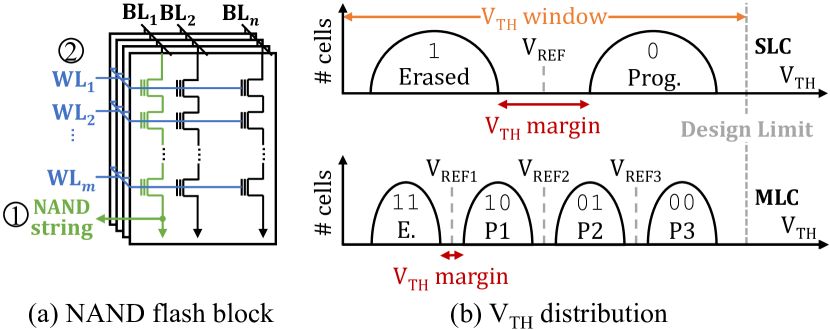
Data Storage Mechanism. A flash cell stores bit data as a function of its threshold voltage (V) level that highly depends on the amount of charge in the cell’s charge trap; the more the electrons in the charge trap layer, the higher the cell’s V level. To increase the storage density, a flash cell can store multiple bits by controlling its V level more precisely, which is called multi-level cell (MLC) technology. Figure 1b compares the V distribution in NAND flash memory when it stores one-bit data per cell using two V states (top) and when it stores two bits per cell using four V states (bottom).
NAND Flash Operations. There are three basic operations to enable access to NAND flash memory: (i) program, (ii) read, and (iii) erase operations. A program operation increases a target cell’s V level by applying a high program voltage (e.g., 20 V). A read operation determines a cell’s V level (i.e., the stored data) by applying a read-reference voltage V to the cell’s control gate; depending on its V level, the cell operates as either an on-switch (V V) or an off-switch (V V). Since a number of flash cells (e.g., ) share a WL, NAND flash memory performs read and program operations at a page granularity (e.g., 16 KiB).
An erase operation decreases a target cell’s V level by applying a high erase voltage V (e.g., 20 V) to the substrate. NAND flash memory performs an erase operation at block granularity, which causes erase latency tBERS to be significantly higher than program latency tPROG and read latency tR (e.g., ms, µs, and µs (cho-isscc-2021, )) but enables high erase bandwidth by concurrently erasing a large number of pages (e.g., more than 2K pages (cho-isscc-2021, )) at once. As a program operation can only increase a cell’s V level, a page needs to be erased first to program data, which is called the erase-before-write property.
2.2. NAND Flash Reliability
NAND flash memory is highly error-prone due to its imperfect physical characteristics. A flash cell leaks its charge (i.e., its V level decreases) over time, which is called retention loss. Reading or programming cells slightly increases the V levels of other cells in the same block (e.g., read/program disturbance (cai-dsn-2015, ; ha-tcad-2016, ; liu-asplos-2021, ; cai-iccd-2013, ; park-dac-2016, ; kim-dac-2017, ; cai-hpca-2017, )). If a cell’s V level shifts beyond the V values (i.e., to adjacent V ranges corresponding to different bit values), reading the cell causes a bit error.
There are two major factors that significantly increase the raw bit-error rate (RBER) of NAND flash memory. First, the high voltage used in program/erase operations physically damages flash cells, making the cells more error-prone. Second, the MLC technique increases RBER because packing more V states within a limited V window narrows the margin between adjacent V states as shown in Figure 1b.
To ensure data reliability, it is common practice to employ strong error-correction codes (ECC). ECC stores redundant bits called ECC parity, which enables detecting and correcting raw bit errors in the codeword. To cope with the high RBER of modern NAND flash memory, modern SSDs use sophisticated ECC that can correct several tens of raw bit errors per 1-KiB data (e.g., low-density parity-check (LDPC) codes (ldpc, )).
3. Motivation
We discuss (i) the importance of optimizing erase operations and (ii) limitations of existing techniques. Table 5 in Appendix summarizes new terminologies defined in this work.
3.1. Negative Impact of Erase Operations
Erase operation significantly affects both SSD lifetime and I/O performance. First, an erase operation is the major source that limits SSD lifetime. The high voltage used in program and erase operations damages flash cells, which makes a block unusable after experiencing a certain number of program and erase (P/E) cycles (e.g., 5K P/E cycles (kim-pe-2021, )) because it can no longer meet the retention requirements for a non-volatile storage medium (e.g., 1-year retention at 30∘C (jedec-1y, )). Program operation also applies a high voltage to flash cells, but prior work has experimentally demonstrated that erase operation accounts for 80% of cell stress due to the significantly longer erase latency compared to program latency (hong-fast-2022, ).
Second, the long erase latency often increases the tail latency of user reads significantly, which is critical for data-center applications (wu-fast-2012, ; kim-fast-2019, ). In fact, the impact of erase operations on the average I/O performance is trivial in modern SSDs (kim-fast-2019, ), since they occur much less frequently compared to read and program operations. For example, a block in modern 3D NAND flash memory consists of more than 2K pages (kim-isscc-2022, ; yuh-isscc-2022, ; kim-isscc-2023, ), so one erase operation occurs after at least 2K page writes (and even more page reads potentially). However, an erase operation may block a page read for an order of magnitude longer time than read latency when it is no longer possible to delay the erase operation under heavy user writes.
3.2. Incremental Step Pulse Erasure (ISPE)
The lifetime and performance impact of erase operations increases even further in modern SSDs, as an erase operation often requires multiple erase loops. As a flash cell experiences more P/E cycles, the cell becomes more difficult to erase (hong-fast-2022, ; kim-pe-2021, ; micheloni2010inside, ). Consequently, an erase operation may fail to sufficiently erase all the cells in a target block, which we call an erase failure. To secure data reliability, it is common practice to employ the Incremental Step Pulse Erasure (ISPE) scheme (ispe, ; hollmer1999erase, ; aritome2015nand, ) that retries to erase the block with an increased erase voltage until completely erasing the block.
Figure 2 shows how a NAND flash chip erases a block via multiple erase loops, each of which consists of two steps: (i) an erase-pulse (EP) step and (ii) a verify-read (VR) step. An EP step (e.g., in Figure 2) applies V to the target block for a fixed amount of time tEP (e.g., 3.5 ms) that is predefined by NAND manufacturers at design time. After each EP step, a VR step (e.g., ) checks if all the cells in the block are sufficiently erased. When EP() (the -th EP step, ) fails to do so, the ISPE scheme performs EP() while progressively increasing V by a fixed amount V. The ISPE scheme repeats this until completely erasing the block, leading to erasure latency tBERS as follows:
| (1) |
where tVR is the VR latency (100 µs), and is the number of erase loops required to completely erase the block.
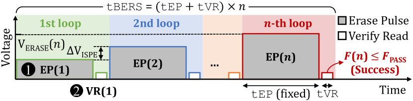
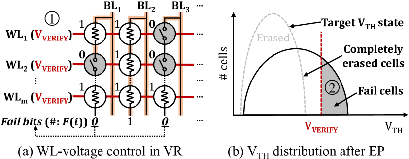
Figures 3a and 3b describe how a NAND flash chip performs a VR step. It simultaneously senses (or activates) all the WLs in the block using a verify voltage V ( in Figure 3a) that is between the erase state and the first program state. If EP() fails, it means that the target block has some cells whose V levels are still higher than V ( in Figure 3b). Such cells would operate as an off-switch during VR() (the -th VR step) because , making the corresponding BLs read as ‘0’ bits, called fail bits. Then, VR() counts (), the number of fail bits after EP(), using on-chip counter logic (micheloni2010inside, ; ito2018sonos, ). It judges that EP() succeeds only when () is lower than a predefined threshold .
3.3. Limitations of Existing Techniques
A large body of prior work (lee-ispass-2011, ; cui-date-2018, ; kang-dac-2018, ; shahidi-sc-2016, ; choi-hpdc-2018, ; guo-ipdps-2017, ; kang-cm-2017, ; pan-hotstorage-2019, ; lee-tcad-2013, ; murugan-msst-2011, ; li-msst-2019, ; dh-tcad-2022, ; jeong-hotstorage-2013, ; jeong-fast-2014, ; jeong-tc-2017, ; wu-fast-2012, ; kim-fast-2019, ; ispe, ) has proposed various optimizations to mitigate the negative impact of erase operations, but none has yet investigated how erase latency should be set to fully exploit the potential of NAND flash memory. Like other memory technologies (e.g., DRAM), modern NAND flash memory also exhibits high process variation that leads to significantly different physical characteristics across flash cells. Prior works have demonstrated varying physical characteristics across WLs (li-micro-2020, ; shim-micro-2019, ; hong-fast-2022, ; wang-acm-2017, ; chen-dac-2017, ; hung-ssc-2015, ; ha-tcad-2016, ) and blocks (kim-pe-2021, ; yen-hpca-2022, ; ha-tcad-2016, ; cai-dsn-2015, ) in modern 3D NAND flash memory. Unfortunately, most existing techniques adopt the ISPE scheme that always uses the same erase-timing parameters (e.g., tEP) for every block. Doing so potentially causes unnecessary erase-induced cell stress, e.g., when a block can be erased more easily compared to the worst-case block.
Limitations of the ISPE Scheme. To understand the potential of optimizing erase latency, we characterize 160 real 3D 48-layer triple-level cell (TLC) NAND flash chips (see §5 for our characterization methodology). We measure , the minimum tBERS to completely erase a block, for 19,200 blocks randomly selected from the 160 chips. Figure 4 shows the cumulative distribution function (CDF) of () across the tested blocks under different P/E-cycle counts ().
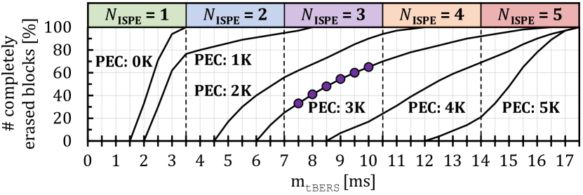
We make three key observations. First, an erase operation requires a number of erase loops in modern SSDs, significantly increasing not only erased-induced cell stress but also erase latency. While all the tested blocks can be erased via a single erase loop at zero PEC, every block requires multiple (24) loops after 2K PEC, causing 24 increases in tBERS when using the ISPE scheme. Second, significantly varies even across blocks that require the same . This clearly shows that a significant number of blocks are over erased under the ISPE scheme, suffering from more erase-induced stress than necessary. If we used the ISPE scheme, 40% of the blocks at 3K PEC would require and thus experience the high erase voltage for 10.5 ms (purple dots in Figure 4), while their values significantly vary. Third, there is considerable erase latency variation when . More than 70% (30%) of the blocks at zero PEC (1K PEC) require only 2.5 ms to be completely erased, which is 29% lower than tBERS in the ISPE scheme (3.5 ms).
We draw two conclusions based on our observations. First, modern NAND flash memory suffers from unnecessarily longer erase latency (and thus more erase-induced cell stress) than actually needed. Second, if it is possible to accurately predict and use for a block, doing so would significantly mitigate the wear-out and long tail latency problems.
Limitations of the State-of-the-Art. To our knowledge, only a few prior works on 2D NAND flash memory (jeong-hotstorage-2013, ; jeong-fast-2014, ; jeong-tc-2017, ; ispe, ) propose to dynamically tune ISPE parameters. Figure 5 depicts the high-level key ideas of (a) DPES (Dynamic Program and Erase Scaling) (jeong-hotstorage-2013, ; jeong-fast-2014, ; jeong-tc-2017, ) and (b) -ISPE (intelligent ISPE) (ispe, ). DPES reduces erase-induced cell stress by decreasing V, which narrows the voltage window for the program states. However, it also requires longer program latency to provide the same level of reliability as the original ISPE scheme by forming much narrower program V states. I-ISPE tracks each block’s to perform only the final erase loop EP() while skipping the previous loops (e.g., EP() and EP() in Figure 5b), which potentially reduces not only the erase-induced stress but also tBERS.
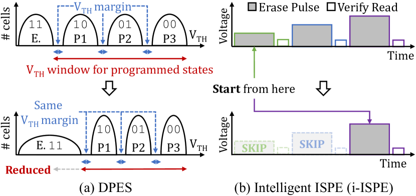
Unfortunately, it is challenging to adopt DPES and -ISPE in modern 3D NAND flash memory due to two reasons. First, erasing 3D flash cells is more difficult compared to 2D cells due to the differences in cell physics and erase mechanisms between them (hong-fast-2022, ). Second, 3D NAND flash memory exhibits higher process variation across cells compared to 2D NAND flash memory (liu-asplos-2021, ; wang-acm-2017, ; chen-dac-2017, ). Such characteristics significantly limit the effectiveness of both DPES and -ISPE in modern NAND flash memory; (i) for DPES, it becomes more challenging to secure the voltage window wide enough for the program states; (ii) for -ISPE, skipping the first erase loops incurs an erase failure more likely, which, in turn, rather requires the next erase loop with a higher V (i.e., more erase-induced stress) compared to the conventional ISPE scheme. We quantitatively evaluate the effectiveness of DPES and -ISPE in modern SSDs in §7.
4. Aero: Adaptive Erase Operation
In this work, we propose Aero (Adaptive ERase Operation) that enhances SSD lifetime and improves I/O performance by applying near-optimal erase latency for each target block.The key idea of Aero is simple. Unlike the ISPE scheme that performs all erase-pulse (EP) steps with fixed latency tEP for every block, Aero dynamically adjusts tEP to be just long enough for complete erasure of a target block. Aero uses the same V() for each EP() as the ISPE scheme, so EP() in Aero may also fail to completely erase the block even without tEP reduction. In such a case, Aero also performs the next EP() while trying to reduce tEP if possible, i.e., when it expects EP() to completely erase the block with reduced tEP. This means that Aero reduces tEP in the final erase loop (i.e., EP()) that completely erases the block, thereby reducing the total erase latency tBERS as follows:
| (2) |
where is the amount of reduction in tEP in EP().
It would be ideal to dynamically optimize both V and tEP at the same time, but we decide to keep using the same V values in the ISPE scheme. This is because it is quite challenging to accurately predict a near-optimal V for a block due to the high process variation in 3D NAND flash memory. Inaccurate V adjustment can cause insufficient or excessive erasure of flash cells as discussed in §3.3, which can rather degrade SSD lifetime and I/O performance. We leave accurate predictions and simultaneous optimizations of both V and tEP to future work.
Fail-bit-count-based Erase Latency Prediction (FELP). A key challenge in Aero is to accurately identify () for a block, i.e., the minimum value of tEP in each EP step (i.e., EP()) just long enough to fully erase all the cells in the block. Even though prior work (chen-trans-2018, ; lue-iedm-2015, ) has experimentally demonstrated a strong correlation between a block’s PEC and erase latency, i.e., the higher the block’s PEC, the longer the latency for erasing the block (jeong-tc-2017, ), PEC alone is insufficient for accurate prediction of near-optimal tEP due to high process variation in modern NAND flash memory. As shown in Figure 4, () significantly varies even across blocks at the same PEC. This suggests that Aero needs a way more effective metric than PEC to figure out more precise erase characteristics (i.e., ()) for individual flash blocks.
Aero addresses the challenge via Fail-bit-count-based Erase Latency Prediction (FELP) that predicts () based on (), the number of fail bits incurred by the previous EP(). Our key intuition is that () can likely be an accurate proxy of () because the more sufficiently the cells are erased by an EP step, the lower the fail-bit count. Commodity NAND flash chips already calculate () for the ISPE scheme as explained in §3.2, so the implementation overhead of FELP is trivial (see §6 for more detailed overhead analysis).
Figure 6a depicts how Aero safely reduces tEP based on FELP. Like the ISPE scheme, Aero also performs a verify-read step VR() after each EP(), which results in (). If () is higher than a threshold (), Aero uses the default tEP for the next EP() considering that there is no room for tEP reduction (e.g., until EP() in Figure 6a). When , Aero reduces tEP, i.e., it predicts and uses () for EP(), such that the lower the value of (), the lower the value of (). Note that Aero provides effectively the same reliability as the ISPE scheme as long as ( ).
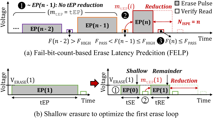
Shallow Erasure. As FELP needs () to predict (), it is difficult for Aero to reduce tEP for the first EP step, i.e., EP(). Optimizing EP() is also important because a block can be completely erased via a single erase loop under many operating conditions. As shown in Figure 4, 76.5% of the tested blocks require only EP() for complete erasure at 1K PEC (i.e., 20% of the maximum PEC).
We enable Aero to optimize EP() by performing it in two steps. Figure 6b describes how Aero reduces the effective tEP for a single-loop erase operation. Instead of using the default tEP (e.g., 3.5 ms) for EP(), Aero first performs a short EP step with the default V(), which we call shallow erasure, for a reduced amount of time tSE (e.g., in Figure 6b). It then performs an additional VR step to obtain the number of fail bits after the shallow erasure (we denote shallow erasure as the 0-th erase loop in the rest of this paper, i.e., EP(), VR(), and () refer to the erase-pulse step, verify-read step, and fail-bit count in shallow erasure, respectively). Finally, Aero performs remainder erasure that also applies the default V() but dynamically adjusts the latency tRE (e.g., ms) based on ().
Leveraging ECC-Capability Margin. Prior work (shim-micro-2019, ; park-asplos-2021, ) has demonstrated that a large ECC-capability margin111The difference between the maximum number of bit errors per codeword that given ECC can correct and the number of bit errors in a codeword. exists in modern SSDs due to two reasons. First, modern SSDs commonly employ strong ECC to cope with the high RBER of NAND flash memory in the worst-case operating conditions (e.g., 1-year retention time at 5K PEC). Second, it is common practice to employ read-retry in modern SSDs (park-asplos-2021, ) to ensure data reliability. When a read page’s RBER exceeds the ECC capability, read-retry repeats reading of the page with adjusted V until it sufficiently lowers RBER, thereby leading to a large ECC-capability margin.
Aero leverages the large ECC-capability margin to reduce tEP more aggressively by increasing the pass threshold in the ISPE scheme. Doing so would likely cause incomplete erasure of a target block, which introduces additional bit errors. However, we hypothesize that Aero can still ensure data reliability in many cases due to three key reasons. First, a block’s reliability degrades as it experiences P/E cycling, so an even larger ECC-capability margin to tolerate the additional errors exists at low PEC. Second, aggressive tEP reduction mitigates erase-induced cell stress, which can compensate for the additional errors as a long-term impact. Third, a majority of additional fail cells due to increased would be programmed to higher V states under the data randomization technique (cha2013data, ; favalli2021scalable, ), e.g., 87.5% in TLC NAND flash memory. It means that such fail cells are unlikely to cause bit error, significantly decreasing the reliability impact of aggressive tEP reduction. To maximize Aero’s benefits without compromising data reliability, we enhance FELP to also consider the expected ECC-capability margin for a target block by keeping the number of additional errors caused by aggressive tEP reduction below the current ECC-capability.
5. Device Characterization Study
To validate our key ideas and hypothesis in §4, we conduct an extensive real-device characterization study.
5.1. Characterization Methodology
Infrastructure. We use an FPGA-based testing platform with a custom flash controller and temperature controller. The flash controller can perform not only basic NAND-flash commands (i.e., for read, program, and erase operations) but also low-level test commands such as GET/SET FEATURE commands (ONFI, ). This feature allows us to modify tEP of each EP() at a granularity of 0.5 ms and obtain () from the chip after VR(). The temperature controller can maintain the operating temperature of the tested chips within ±1∘C of the target temperature, thus minimizing unintended RBER variations potentially caused due to unstable temperature.
Methodology. We characterize 160 real 48-layer 3D TLC NAND flash chips from Samsung (kang-isscc-2016, ) in which the default ms. To minimize the potential distortions in our results, for each test scenario, we evenly select 120 blocks from each chip at different physical locations and test all WLs in each selected block. We test a total of 3,686,400 WLs (11,059,200 pages) to obtain statistically significant results.
We test the chips while varying PEC and retention time. Unless specified otherwise, we increase a block’s PEC by programming every page in the block using a random pattern and erasing the block with the default tEP in every erase loop. We follow the JEDEC industry standard (jedec, ) for an accelerated lifetime test to analyze the reliability under the worst-case operating conditions. For example, to emulate a 1-year retention time at 30∘C, we bake the chips at 85∘C for 13 hours following the Arrhenius’ law (arr, ).
To identify a block’s (i.e., and ()), we erase the block using a modified ISPE scheme (m-ISPE) that we design by modifying the original ISPE scheme in two aspects. First, we reduce the fixed latency tEP for each EP() from 3.5 ms to 0.5 ms, i.e., we split an erase loop in the ISPE scheme into seven shorter loops. Second, we increase V for every seven erase loops (not for every loop) to effectively emulate the ISPE scheme. If a block requires loops under m-ISPE, we estimate and of the block under the ISPE scheme. Even though the m-ISPE scheme requires six additional ramping-up/down steps to charge/discharge voltage and VR steps for each erase loop compared to the original ISPE scheme, its reliability impact is negligible; for our 160 tested chips, the m-ISPE scheme hardly increases the average RBER (by less than 1%) compared to the original ISPE scheme, under 1-year retention time at 5K PEC.
5.2. Fail-Bit Count vs Near-Optimal Erase Latency
To validate the feasibility of FELP, we analyze the relationship between the minimum erase latency and fail-bit count. We measure each block’s and () while tracking () in every EP() under the m-ISPE scheme. Figure 7 depicts the maximum value of () within the blocks that have the same (), when we progressively increase tEP by 0.5 ms in the final EP step (i.e., EP()).
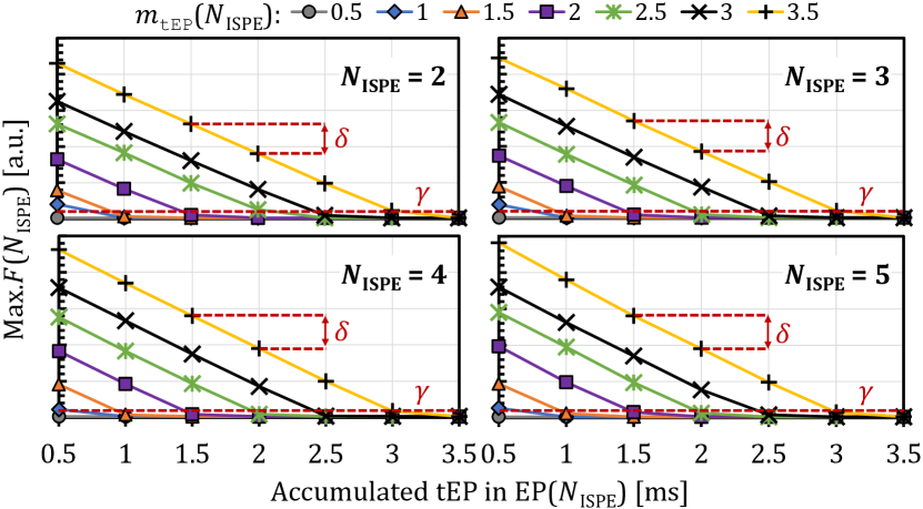
We make two key observations. First, the fail-bit count almost linearly decreases as tEP increases. While the negative correlation between () and tEP is expected in §4, the correlation is significantly high and consistent; increasing tEP by 0.5 ms decreases () by almost the same amount () in all tested blocks with different and () values. This suggests that (i) erase latency has a linear impact on the degree of erasure under the same erase voltage, and (ii) NAND manufacturers carefully set V values (i.e., V() and V) in the ISPE scheme to avoid excessive increases in erase-induced cell stress and erase latency. Second, when ms, () is quite consistent at a certain value () in all test scenarios. The result suggests that the lower the cell’s V level, the more difficult it becomes to further reduce the V level.
Our observations highlight the high potential of FELP. To confirm this, we analyze how a block’s () varies depending on its (). Figure 8 depicts the probability of () at different across the fail-bit ranges that we set based on and from Figure 7. A box at (, ) in Figure 8 represents the probability (in grayscale) that a block requires ms for complete erasure when its () belongs to -th fail-bit range. We also plot the fraction of blocks that belong to the -th fail-bit range (top). Note that for the same , the sum of all fractions (top) is 100%, and the sum of all probabilities at the same -th fail-bit range (bottom) is 100%.
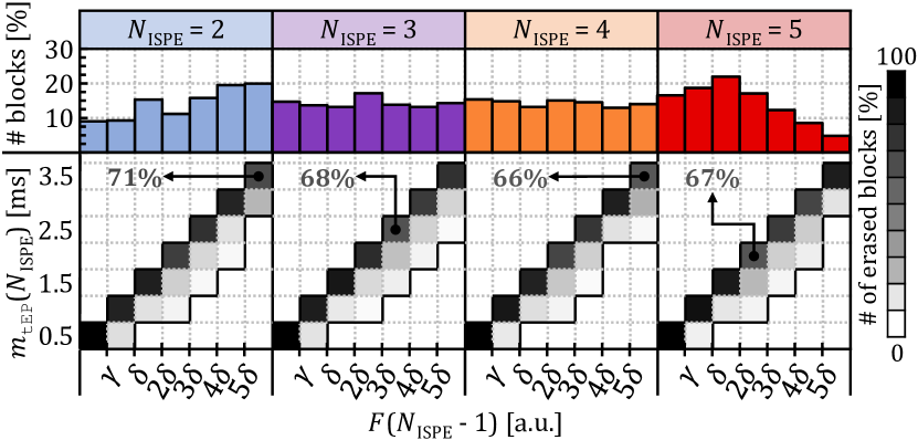
We make two key observations. First, FELP is highly effective at predicting (). A majority of blocks (e.g., in ) in the same fail-bit range require the same () under all different cases. Even though every fail-bit range contains some blocks whose () is lower compared to the majority of blocks, the fraction is quite low (e.g., in ) in all the fail-bit ranges and cases. Second, () is distributed across blocks quite evenly in all cases. This highlights again that () is an accurate proxy of (), given that () also significantly varies across blocks in a wide range as shown in Figure 4.
Based on our observations, we draw two conclusions. First, Aero can accurately predict the minimum erase latency using FELP, even for blocks that have varying erase characteristics. Second, the implementation of FELP requires only identifying two values for fail-bit ranges, e.g., and in Figures 7 and 8, which can be done using our characterization methodology.
5.3. Shallow Erasure: Feasibility & Parameter Setting
We validate the feasibility of shallow erasure and explore a good latency value. Figure 9 shows the distribution of () across blocks under different 0.5 ms, 1 ms, 1.5 ms, 2 ms and 0.1K, 0.5K. We confirm that all the tested blocks in the -th fail-bit range can be completely erased via subsequent remainder erasure with ms.
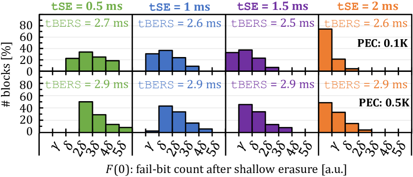
We make three key observations from Figure 9. First, shallow erasure enables Aero to reduce tEP for EP(). A large fraction of blocks can be completely erased with lower latency than the default tEP (80%, 85%, 86%, 88% for 0.5 ms, 1 ms, 1.5 ms, 2 ms). Second, tSE does not significantly affect the average tBERS. We annotate the average tBERS for each tSE case in Figure 9, which shows their small variation (10%). Third, with a low probability, shallow erasure may cause a block to be over-erased. For example, at 0.5K PEC, 2% blocks can be erased with tBERS ms when tSE 1 ms (the second fail-bit range), while there exist no such blocks in the other tSE cases.
Based on our observations, we conclude that Aero can significantly optimize not only multi-loop erase operations but also single-loop erase operations using shallow erasure. For our tested chips, we decide to set tSE ms to minimize the probability of an over-erased block, which reduces both erased-induced stress for 85% of blocks and the average erase latency by 21% for single-loop erase operations.
5.4. Reliability Margin for Aggressive tEP Reduction
To identify the ECC-capability margin for more aggressive tEP reduction, we analyze the reliability impact of insufficient erasure. We measure of each block, i.e., the maximum RBER within the pages in the block under 1-year retention time at 30∘C, when we erase the block in two different ways. First, we completely erase the block by performing erase loops with (). Second, we insufficiently erase the block by performing only () erase loops, which results in . Figure 10 depicts the maximum value of within the tested blocks when we program the blocks (a) after complete erasure and (b) after insufficient erasure. For Figure 10b, we group the tested blocks depending on their and fail-bit range. We also plot (i) the ECC capability at 72 bits per 1 KiB and (ii) the RBER requirement at 63 bits per 1 KiB to reflect sampling errors (i.e., a block is considered unusable if its to incorporate a safety margin into the ECC capability).
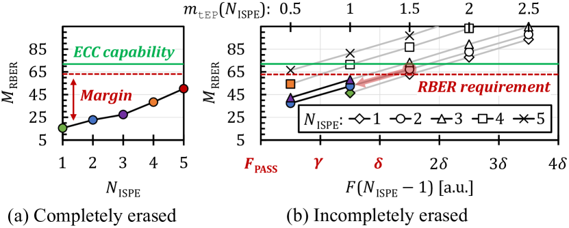
We make two key observations. First, we observe a large reliability margin (i.e., ) that can potentially be used to further reduce tEP especially in the early lifetime stage of blocks. As shown in Figure 10a, when a block is completely erased, there always exists a positive reliability margin for all values up to 47 bit errors (). Second, it is possible to further reduce tEP without compromising reliability in many operating conditions. As shown in Figure 10b, using an insufficiently-erased block still meets the RBER requirement (i.e., ) if either of the following two conditions is met: [C1: and ] and [C2: and ]. This means that we can skip the final erase loop in such cases, thereby further increasing the amount of tEP reduction even higher than the default tEP in the ISPE scheme, i.e., can be larger than tEP in (2). Note that Aero can further reduce () even if neither of [C1] and [C2] is met because increasing tEP by 0.5 ms in EP() decreases () by as demonstrated in §5.2. For example, a block requires ms for complete erasure when and , but using ms in EP() can still meet the RBER requirement since doing so would decrease below 63 (see the arrow in Figure 10 b).
We conclude that Aero can significantly mitigate the negative impact of erase operations by leveraging not only the high process variation but also the large ECC-capability margin present in modern SSDs. Table 1 shows the final () model that we construct; each cell’s value ‘ / ’ indicates () when Aero leverages only the process variation () and when also leveraging the ECC-capability margin ().
| () | ||||||||
| 1 | 0.5 / 0 | 1 / 0 | 1.5 / 0.5 | 2 / 1 | 2.5 / 1.5 | 2.5 / 2 | 2.5 / 2.5 | 2.5 / 2.5 |
| 2 | 0.5 / 0 | 1 / 0 | 1.5 / 0.5 | 2 / 1 | 2.5 / 1.5 | 3 / 2 | 3.5 / 2.5 | 3.5 / 3 |
| 3 | 0.5 / 0 | 1 / 0 | 1.5 / 0.5 | 2 / 1 | 2.5 / 1.5 | 3 / 2 | 3.5 / 2.5 | 3.5 / 3 |
| 4 | 0.5 / 0 | 1 / 0.5 | 1.5 / 1 | 2 / 1.5 | 2.5 / 2 | 3 / 2.5 | 3.5 / 3 | 3.5 / 3.5 |
| 5 | 0.5 / 0.5 | 1 / 1 | 1.5 / 1.5 | 2 / 2 | 2.5 / 2.5 | 3 / 3 | 3.5 / 3.5 | 3.5 / 3.5 |
5.5. Applicability of Aero for Other Types of Chips
We expect that the key ideas of Aero are generally applicable to a wide range of NAND flash chips other than the chips used for our characterization study due to three reasons. First, our chips well represent modern 3D NAND flash memory because most commercial chips including SMArT/TCAT/BiCS have similar structures and cell types, e.g., vertical channel structures, gate-all-around cell transistors, and charge-trap type flash cells (micheloni2010inside, ; micheloni3d, ; aritome2015nand, ), sharing key device characteristics like operation mechanisms and reliability characteristics. Second, the erase mechanism of NAND flash memory has not changed significantly for more than a decade. For example, the ISPE scheme has been used since 2D SLC NAND flash memory (micheloni2010inside, ; aritome2015nand, ). Third, AERO does not rely on chip-specific behaviors but leverages inherent erase characteristics, e.g., the more completely the cells within a block are erased, the lower the fail-bit count of the block.
To support our hypothesis, we characterize two additional types of NAND flash chips, (i) 2x-nm 2D TLC NAND flash chips (vatto-anandtech-2012, ) and (ii) 48-layer 3D MLC NAND flash chips (tallis-anandtech-2012, ) from Samsung. We use the same methodology as other device characterizations. Figure 11 shows (a) the values of and for all tEP and cases (box plot) and (b) the maximum value of within the tested block after insufficient erasure.
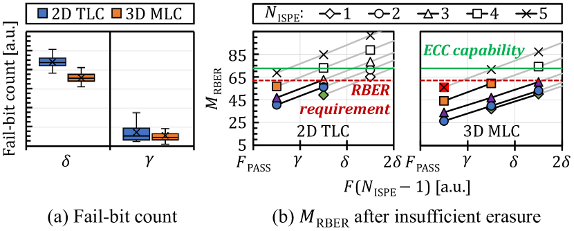
We make two key observations. First, although the exact values of and slightly vary depending on the chip type, they are quite consistent within the same type of chips across all tested cases as shown in Figure 11a. This clearly shows that the strong linear relationship between the fail-bit count and accumulate tEP also holds in the chips additionally tested. Second, as shown in Figure 11b, the reliability impacts of insufficient erasure in the 2D TLC and 3D MLC chips exhibit highly similar trends to those in the 3D TLC chips (cf. Figure 10b),222The results shown in Figures 10b and 11b, which are remarkably similar, might seem counter-intuitive because it is well known that 3D NAND flash memory exhibits better reliability compared to 2D NAND flash memory (luo-acm-2018, ). Nevertheless, commodity 3D NAND flash chips provide a similar level of reliability to 2D chips because the better reliability characteristics of 3D NAND flash memory are used to avoid write-performance degradation over 2D NAND flash memory. Since its first development, a majority of 3D NAND flash memory has been designed to contain two planes (old_3d, ), whereas state-of-the-art 2D chips consist of four planes (recent_2d, ). The decrease in the number of planes per chip would inevitably limit the bandwidth of multi-plane writes in 3D NAND flash chips to be around twice lower compared to 2D chips if the same program-timing parameters were used (e.g., tPROG 1.2 ms in 2D NAND flash memory (recent_2d, )). To avoid this, manufacturers have reduced the program latency of 3D NAND flash memory by trading its better reliability, which enables sustaining (or even improving) the write bandwidth of 3D chips without compromising reliability compared to 2D chips. suggesting the high feasibility of aggressive tEP reduction also in the two types of chips. We conclude that Aero can be used for a wide range of chips with the same methodology we use to construct the tEP model for our tested chips (Table 1).
6. Design and Implementation
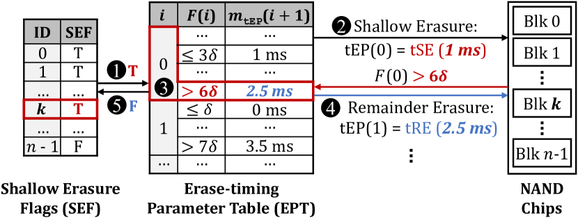
We design AeroFTL, an Aero-enabled flash translation layer (FTL), by extending the conventional page-level FTL (gupta-2009-asplos, ) with two key data structures: (i) Erase-timing Parameter Table (EPT) and (ii) Shallow Erasure Flags (SEF). The EPT is a simple table to stores () for each EP() depending on (), which can be built via offline profiling of target chips as in §5 (Table 1). The SEF is a bitmap that keeps track of whether a block needs shallow erasure or not. Every bit in the SEF is initially set to ‘0’, which is translated to TRUE. Doing so enables AeroFTL to always perform shallow erasure for a fresh block that has experienced no P/E cycle.
Figure 12 illustrates how AeroFTL dynamically adjusts erase latency. For erasing a block whose index (or ID) is , it first looks up the corresponding (-th) bit in the SEF ( in Figure 12). If the flag bit is TRUE, AeroFTL performs shallow erasure by changing the target chip’s tEP to tSE with a SET FEATURE command. Then it queries the EPT with () that can be obtained via a GET FEATURE command. Based on the query result, AeroFTL sets the chip’s tEP and performs remainder erasure. If the remainder erasure cannot reduce the effective latency of the first erase loop, AeroFTL sets the corresponding bit in the SEF to ‘1’ that is translated to ‘FALSE’. Doing so allows AeroFTL to skip shallow erasure for the block in future, but directly performs EP() with the default tEP, thereby avoiding the unnecessary VR(). The remaining process is straightforward. If an erase loop fails, AeroFTL performs the next loop while adjusting the chip’s tEP based on the value obtained from the EPT.
Misprediction Handling. While not observed in our real-device characterization, it is possible that Aero fails to completely erase outlier blocks (which could potentially be missed in the set of blocks we experimentally test) with reduced latency. AeroFTL can easily handle such a misprediction because it always checks () anyways to verify whether a block is completely erased. If AeroFTL detects a misprediction, it repeats an additional EP step with appropriate V and tEP until completely erasing the block; it uses the same V if the accumulated latency is lower than the default tBERS while increasing V otherwise. Despite Aero’s low misprediction rate, we evaluate its potential impact in §7.
Impact on ECC-Decoding Latency. Aggressive tEP reduction in Aero can potentially increase ECC-decoding latency (e.g., in LDPC (ldpc, )), but its performance impact is limited due to two reasons. First, it is common practice to limit the number of iterations for hard-decision ECC decoding (vahabzadeh-fms-2016, ; declercq-fms-2019, ) so that ECC-decoding latency (e.g., 8 µs (ldpc_decision, )) can be hidden by page sensing and data transfer. Second, the RBER requirement conservatively set in Aero (e.g., 63 bits per 1 KiB) ensures a low hard-decision failure rate (e.g., (ldpc_decision, )), hardly causing additional soft-decision LDPC decoding.
Multi-Plane Operations. Multi-plane operation is a widely used feature in modern NAND flash-based SSDs to improve I/O performance (micheloni2010inside, ; flash-cosmos, ; genstore, ). A typical NAND flash chip consists of multiple (e.g., 2 or 4) planes, each of which has its own flash cell array and page buffer. Planes in the same chips can operate concurrently if certain conditions are met, e.g., only the same type of NAND flash operations (i.e., read, program, or erase operations) can be performed in parallel across planes in a chip because they share part of peripheral circuitry. Multi-plane operation can increase chip throughput linearly with the number of planes per chip, thereby significantly improving SSD-internal parallelism and I/O performance.
Aero can work with multi-plane erase operations due to two reasons. First, a NAND flash chip can individually set tEP for each target block of a multi-plane erase operation. Second, as soon as a target block is completely erased, it is possible to inhibit the block from being further erased by the subsequent erase loops during a multi-plane erase operation. Although the worst block (which requires the longest erase latency) in target planes determines the latency of a multi-plane erase operation, Aero can still sustain lifetime benefit and reduce tail latency by erasing each block in target planes only with necessary loops and times.
Implementation Overhead. AeroFTL requires only two small changes to conventional SSDs. First, AeroFTL can use GET/SET FEATURE commands to obtain () and adjust tEP for each EP(), respectively, thereby requiring no change to commodity NAND flash chips. Second, the storage overhead for the EPT and SEF is trivial. The EPT needs to keep entries, where and indicate the number of possible tEP values and the maximum number of erase loops, respectively. In our current design, the EPT has 35 entries ( and ), which requires only 140 bytes even when using a 32-bit value per entry. The SEF needs to keep 1-bit information for each block. In our tested chips, the block size is around 10 MB, so the SEP’s storage overhead is % () of SSD capacity, e.g., 12.5 KB for a 1-TB SSD. Note that modern SSDs contain several GB of internal DRAM (ssd_dram, ), so the storage overhead is negligible.
7. Evaluation
We evaluate the effectiveness of Aero at improving the lifetime and performance of modern NAND flash-based SSDs.
7.1. Evaluation Methodology
We evaluate Aero in two ways. First, we characterize 160 real 3D TLC NAND flash chips to assess the lifetime enhancement of Aero. Unless specified otherwise, we follow the real-device characterization methodology explained in §5.1. Second, we evaluate the impact of Aero on I/O performance using MQSim (tavakkol-fast-2018, ), a state-of-the-art SSD simulator.
We compare five different erase schemes: (i) Baseline, (ii) i-ISPE, (iii) DPES, (iv) AERO, and (v) AERO. Baseline is the conventional ISPE scheme explained in §3.2. I-ISPE is the intelligent ISPE scheme (ispe, ) explained in §3.3, which directly performs EP() while skipping the previous EP steps if the block has been completely erased by EP() in the most-recent erase operation. DPES (explained in §3.3) mitigates erase stress by reducing erase voltage V by 8–10% at a cost of 10–30% increase in write latency tPROG (jeong-tc-2017, ). Since DPES is only applicable until 3K PEC in our tested chips (i.e., no matter how much tPROG increases, reducing V can no longer meet the reliability requirements), we use the same V and tPROG values as in Baseline after 3K PEC. AERO and AERO dynamically adjust tEP for each EP() at a granularity of 0.5 ms based on (). AERO does not exploit the ECC-capability margin, i.e., it is more conservative in tEP reduction compared to AERO that adopts all optimizations in §4.
Simulation Methodology. We extend MQSim in two aspects to model the behavior of modern SSDs more faithfully. First, we modify the NAND flash model of MQSim to emulate the erase characteristics of our 160 tested chips. To this end, during our real-device characterization study in §5, we keep track of erase-related metadata such as the minimum erase latency, fail-bit count, and PEC for every tested block. For simulation, we then randomly select tested blocks and assign their metadata to each of the simulated blocks in MQSim. Because MQSim already tracks PEC, a simulated block can accurately emulate the erase characteristics of the corresponding real block at a given PEC by simply looking up the metadata. Second, we optimize the request scheduling algorithm of MQSim to service user I/O requests with a higher priority over SSD-internal read/write/erase operations, e.g., suspending an ongoing erase operation (kim-fast-2019, ). Table 2 summarizes the configurations of the simulated SSDs. We configure the architecture and timing parameters of simulated SSDs to be close to commodity high-end SSDs (e.g., (samsung, )).
| SSD | Capacity: 1024 GB | Interface: PCIe 4.0 (4 lanes) |
| GC policy: greedy (chang-2002-rtas, ) | Overprovisioning ratio: 20% | |
| # of channels: 8 | # of chips per channel: 2 | |
| NAND Flash Chip | # of planes per chip: 4 | # of blocks per plane: 497 |
| # of pages per block: 2,112 | Page size: 16 KB | |
| MLC technology: TLC | tR: 40 µs (cho-isscc-2021, ) | |
| tEP (Aero): 0.5 ms – 3.5 ms | tEP: 3.5 ms (cho-isscc-2021, ) | |
| tSE (Aero): 1 ms | tPROG: 350 µs (cho-isscc-2021, ) | |
| tPROG: 385 µs (DPES, 0.5K PEC), 455 µs (DPES, 2.5K PEC) | ||
For our performance evaluation, we study eleven workloads selected from two benchmark suits, Alibaba Cloud Traces (alibaba, ) and Microsoft Research Cambridge (MSRC) Traces (msr, ), which are collected from real datacenter and enterprise servers. For MSRC traces, we reduce the inter-request arrival time by 10, as similarly done in a large body of prior work to evaluate more realistic workloads (tavakkol-fast-2018, ; nadig-isca-2023, ; hong-fast-2022, ; yen-hpca-2022, ; mix_liu_1, ; mix_liu_2, ; mix_lv, ; mix_wu, ; jeong-tc-2017, ; jeong-fast-2014, ; jeong-hotstorage-2013, ). Table 3 summarizes the I/O characteristics of the workloads used for our evaluation.
| Benchmark | Trace | Abbr. | Read Ratio | Avg. Req. Size | Avg. Inter Req. Arrival Time |
| Alibaba Cloud (alibaba, ) | ali_32 | ali.A | 7% | 54 KB | 16.3 ms |
| ali_3 | ali.B | 52% | 26 KB | 111.8 ms | |
| ali_12 | ali.C | 69% | 38 KB | 57.9 ms | |
| ali_121 | ali.D | 78% | 18 KB | 13.8 ms | |
| ali_124 | ali.E | 95% | 36 KB | 5.1 ms | |
| MSR Cambridge (msr, ) | rsrch_0 | rsrch | 9% | 9 KB | 421.9 ms |
| stg_0 | stg | 15% | 12 KB | 297.8 ms | |
| hm_0 | hm | 36% | 8 KB | 151.5 ms | |
| prxy_1 | prxy | 65% | 13 KB | 3.6 ms | |
| proj_2 | proj | 88% | 42 KB | 20.6 ms | |
| usr_1 | usr | 91% | 49 KB | 13.4 ms |
7.2. Impact on SSD Lifetime
To evaluate the lifetime enhancement of Aero, we measure () for each real tested block, the maximum RBER within the pages in the block, while varying PEC under 1-year retention at 30∘C. We construct five sets of 120 blocks randomly selected from 160 real 3D NAND flash chips and test each set while increasing PEC using one of the five erase schemes. Figure 13 depicts the average across the tested blocks under different PEC.
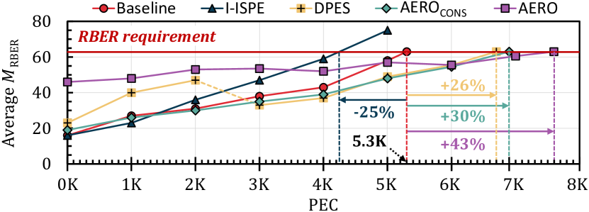
We make four key observations. First, both AERO and AERO significantly improve SSD lifetime over Baseline. The average increases at a much slower rate with PEC in AERO and AERO compared to in Baseline, which clearly shows the high effectiveness of the erase latency reduction in Aero at lowering erase-induced cell stress. The slower increase in , in turn, enables a block to meet the RBER requirement at higher PEC in AERO (7.6K) and AERO (6.9K) compared to Baseline (5.3K), significantly enhancing SSD lifetime by 43% and 30%, respectively.
Second, AERO further improves SSD lifetime considerably over AERO (by 10%) without compromising data reliability. This highlights the high effectiveness of leveraging the reliability margin to reduce erase latency more aggressively. The aggressive tEP reduction causes high even for fresh blocks (i.e., () in AERO) but greatly slows down increase (() () 9.5), showing its high long-term benefits.
Third, DPES also improves SSD lifetime considerably (by 26%) compared to Baseline, but its benefits are limited compared to both AERO and AERO. Like AERO, DPES exhibits rather high due to V reduction until 3K PEC, which, in turn, enables its to increase more slowly later. However, DPES’s benefits are limited due to (i) its limited applicability (until 3K PEC) as well as (ii) its write-performance overheads.
Fourth, i-ISPE accelerates RBER increase, which, in turn, rather decreases SSD lifetime. In fact, i-ISPE provides the lowest among the compared SSDs at 0K, 1K where it is relatively easy to completely erase a block compared to at high PEC. However, it frequently incurs an erase failure as PEC increases, causing more erase-induced cell stress as explained in §3.3. Consequently, i-ISPE leads to shorter SSD lifetime by 25% even compared to Baseline, which shows its limited applicability in modern SSDs.
7.3. Impact on I/O Performance
Average I/O Performance. To evaluate the performance impact of Aero, we first compare average I/O performance of the five SSDs in three aspects: (i) read latency, (ii) write latency, and (iii) I/O throughput (IOPS, input/output operations per second). Table 4 summarizes the three average performance values in i-ISPE, DPES, AERO, and AERO that are normalized to Baseline, on average across all the workloads. We observe that all the evaluated SSDs except for DPES show almost the same average performance for all the workloads and 0.5K, 2.5K, 4.5K. This is because modern SSDs perform erase operations much less frequently compared to reads and writes as explained in §3.1. Unlike the other SSDs, DPES significantly increases average write latency and IOPS at 0.5K, 2.5K, i.e., when the DPES scheme is applicable. Note that we do not evaluate i-ISPE at 4.5K PEC, as it cannot meet the RBER requirement before PEC reaches 4.5K as shown in Figure 13.
| Erase Scheme | Geomean of Norm. Avg. Perf. at 0.5K, 2.5K, 4.5K | ||
| Norm. Avg. | Norm. Avg. | Norm. Avg. | |
| Read Latency [%] | Write Latency [%] | IOPS [%] | |
| I-ISPE | 100.0, 99.8, N/A | 100.0, 100.0, N/A | 100.0, 100.1, N/A |
| DPES | 100.4, 101.3, 99.9 | 110.8, 135.6, 100.0 | 95.7, 87.8, 100.0 |
| AERO | 99.9, 99.7, 99.7 | 99.8, 99.9, 99.8 | 100.2, 100.3, 100.3 |
| AERO | 99.9, 99.6, 99.7 | 99.8, 99.8, 99.9 | 100.2, 100.4, 100.3 |
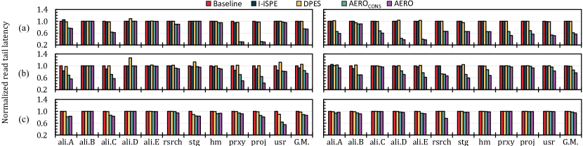
Read Tail Latency. We evaluate the impact of Aero on SSD read tail latency that is critical in modern enterprise or datacenter server systems (decandia-sosp-2007, ; gunawi-2016-socc, ). Figure 14 represents the 99.99th and 99.9999th percentile read latencies ( and , respectively) in the five simulated SSDs at 0.5K, 2.5K, 4.5K (all values are normalized to Baseline).
We make six observations from Figure 14. First, AERO (AERO) significantly reduces and compared to Baseline by 22% (18%) and 26% (20%), respectively, on average across all the evaluated workloads and PEC. Second, Aero achieves higher performance benefits at lower PEC while still providing considerable performance improvements at high PEC. AERO (AERO) outperforms Baseline by 35%, 24%, 9% (32%, 15%, 7%) when 0.5K, 2.5K, 4.5K, reducing and compared to Baseline by 26%, 25%, 13% (26%, 16%, 11%) and 43%, 23%, 5% (39%, 14%, 2%) when 0.5K, 2.5K, 4.5K. This is because Aero only reduces tEP in EP(), which has a higher impact when is low. The high benefits at 0.5K PEC (Figure 14a) also clearly show the high effectiveness of shallow erasure, given that for most blocks. Third, Aero improves I/O performance also when the workload is read-dominant (e.g., ali.E and usr). This highlights the importance of optimizing the latency of erase operations that dictate read tail latency. Fourth, at 2.5K PEC, AERO considerably reduces and over AERO by 11% on average (up to 34% and 22%, respectively), which shows the effectiveness of leveraging the ECC-capability margin for further tEP reduction. Fifth, AERO also reduces and over i-ISPE by 26%, 20% and 43%, 23% at 0.5K, 2.5K, respectively, on average across all the evaluated workloads. At 0.5K PEC, both AERO and i-ISPE can completely erase almost every block via a single loop for which only Aero can reduce tBERS using shallow erasure. Even though i-ISPE can also decrease (and thus tBERS) to less than 2 (7 ms) at 2.5K PEC by skipping the first erase loops, AERO achieves higher benefits due to aggressive tEP reduction and slower increase (92% of the blocks can be erased within two erase loops at 2.5K PEC). Sixth, AERO reduces and over DPES by 22% and 25%, respectively, on average across all the evaluated workloads and PEC. In particular, at 2.5K PEC, of DPES rather often increases by 5% compared to Baseline due to the increase in tPROG, whereas AERO causes no performance degradation but provides 25% benefits on average across all worloads.
Impact of Erase Suspension. To better understand Aero’s performance benefits, we evaluate the impact of erase suspension on read tail latency in AERO and AERO. Figure 15 shows , and in AERO and AERO at 0.5K, 2.5K, 4.5K, averaged across all workloads, when we disable the erase suspension scheme (kim-fast-2019, ) (we also plot the results with erase suspension for comparison). All values are normalized to Baseline without erase suspension.
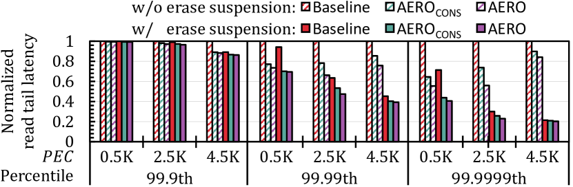
We make two key observations. First, Aero significantly improves I/O performance also when erase suspension is disabled. AERO provides high benefits over Baseline, e.g., 45%, 44%, 16% reductions in at 0.5K, 2.5K, 4.5K. Second, the performance benefits of Aero become even higher when disabling erase suspension. For example, when erase suspension is enabled, AERO achieves 43%, 23%, 5% reduction in over Baseline at 0.5K, 2.5K, 4.5K, which is 2%, 21%, 11% lower compared to when erase suspension is disabled. This is because, without erase suspension, a page read must wait for the completion of the entire ongoing erase loop, which significantly increases the impact of erase latency on read tail latency compared to when the ongoing erase loop can be suspended. Note that, even though the erase suspension scheme often shows a higher reduction in read tail latency to Aero when they are applied exclusively, it does not diminish the value of Aero. This is because Aero also improves SSD lifetime significantly and can be easily combined with erase suspension to further reduce read tail latency.
7.4. Sensitivity Analysis
Impact of Misprediction. Even though we have observed no misprediction in our real-device characterization, we analyze the performance and lifetime impact of misprediction in Aero since it is improbable but not impossible to happen. To this end, we make two assumptions on Aero’s misprediction behavior based on our real-device characterization results. First, we consider each erase-latency prediction of Aero as an independent trial with a constant failure (i.e., misprediction) rate for all blocks and operating conditions. This is because, although reliability characteristics significantly vary across blocks and operating conditions, Aero can accurately predict the minimum erase latency for all tested chips, blocks, and operating conditions as demonstrated in §5 (i.e., we observe nothing suggesting that certain chips, blocks, or operating conditions are more prone to Aero’s misprediction). Second, we assume that AERO performs an additional 0.5-ms EP step for each misprediction. We believe that 0.5 ms is long enough for Aero to handle a misprediction because the target block must be largely (though not completely) erased even when a misprediction happens (otherwise, Aero would not have reduced erase latency). Figure 16 shows how Aero’s misprediction rate affects its benefits in SSD lifetime (left) and read tail latency (right).
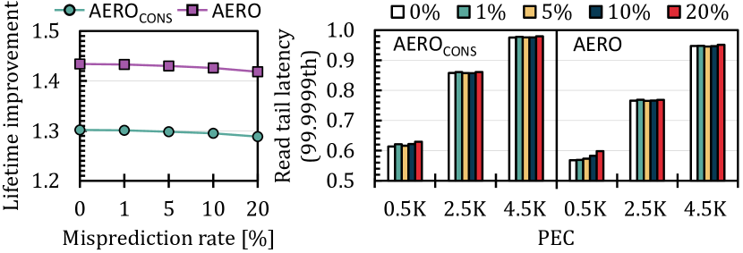
We make two key observations. First, Aero is highly effective at improving both SSD lifetime and I/O performance even when mispredictions happen. Even under a high misprediction rate of 20%, AERO (AERO) provides 42% (29%) and 40% (37%) improvements over Baseline in SSD lifetime and read tail latency (at 0.5K PEC), respectively. This is because AERO and AERO are still able to reduce erase latency when a misprediction happens, i.e., the amount of erase-latency reductions (e.g., up to 3.5 ms) is higher than the misprediction penalty (e.g., 0.5 ms), in many cases. Second, the performance impact of misprediction becomes even smaller as PEC increases. Compared to when no misprediction occurs, 20% misprediction rate causes small increases (5.3% and 2.6% at 0.5K PEC in AERO and AERO, respectively) in , which significantly decreases (to 0.4% for both) at 4.5K PEC. This is because the total erase latency severely increases with PEC, thereby making the performance impact of misprediction much smaller.
Impact of Reliability Margin. We evaluate how AERO’s benefits change depending on the reliability margin that directly affects the effectiveness of aggressive tEP reduction. To this end, we evaluate the performance and lifetime benefits of AERO while reducing the reliability requirement (i.e., the maximum raw bit errors per 1 KiB) to 40 and 50 (from 63), which can happen when using weaker ECC. Figure 17 shows SSD lifetime (left) and read tail latency (right) of AERO and AERO under different reliability requirements, normalized to Baseline. Note that the lifetime of Baseline and AERO also degrades as the reliability requirement decreases (because they can tolerate fewer errors).
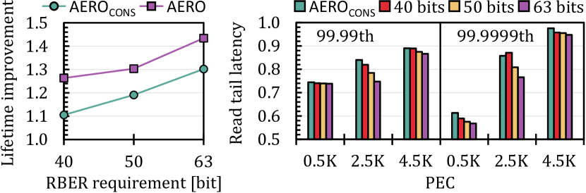
We observe that AERO can still improve SSD lifetime when the RBER requirement decreases considerably. Although the chance for aggressive tEP reduction significantly decreases when the RBER requirement is 40 bits (only if and () as shown in Figure 10b), it still allows 14% lifetime enhancement over AERO. In particular, AERO achieves the highest benefit at 2.5K PEC. This is because AERO can completely erase most blocks with , which allows it to aggressively reduce tEP for many blocks ( and () in Figure 10b).
Based on the key observations in our evaluation, we conclude that Aero is highly effective at improving both SSD lifetime and I/O performance for many real-world workloads under varying operating conditions. We believe that Aero is a promising solution, considering its high lifetime and performance benefits that come with almost negligible overheads.
8. Related Work
To our knowledge, this work is the first to dynamically adjust erase latency by leveraging varying erase characteristics across blocks, providing significant lifetime and performance benefits for modern SSDs. We already discussed and compared to the state-of-the-art techniques (ispe, ; jeong-tc-2017, ) closely related to Aero (§3.3 and §7). We briefly describe other related work that aims to improve the lifetime and performance of SSDs.
Mitigating Negative Impact of Erase Operation. A large body of prior work has proposed various techniques to mitigate the negative impact of erase operations on SSD lifetime and I/O performance. Many studies have optimized the algorithms of internal SSD management tasks, e.g., garbage collection (lee-ispass-2011, ; cui-date-2018, ; kang-dac-2018, ; shahidi-sc-2016, ; choi-hpdc-2018, ; guo-ipdps-2017, ; kang-cm-2017, ; pan-hotstorage-2019, ; lee-tcad-2013, ) and wear leveling (murugan-msst-2011, ; li-msst-2019, ; dh-tcad-2022, ), to reduce the number of erase operations invoked for servicing the same amount of user writes. To prevent an erase operation from delaying latency-sensitive reads for a long time, some studies propose to suspend an ongoing erase operation to service user reads (and resume the erase operation after completing the reads) (wu-fast-2012, ; kim-fast-2019, ). Despite the significant lifetime and performance improvements made by the prior research, the existing techniques erase a block using the conventional ISPE scheme, thereby causing over-erasure of blocks frequently. Aero introduces only small implementation overheads and thus can be easily integrated into the existing techniques to further improve the lifetime and performance of modern SSDs.
Process Variation. Many prior studies (yen-hpca-2022, ; shim-micro-2019, ; hong-fast-2022, ; wang-acm-2017, ; chen-dac-2017, ; hung-ssc-2015, ; kim-pe-2021, ) leverage varying physical characteristics across flash cells to optimize modern SSDs. Hong et al. (hong-fast-2022, ) propose a new erase scheme that applies a low voltage to error-prone WLs selectively (while keeping the same voltage for the other WLs), which makes only a small fraction of weak WLs (temporarily) unusable but eventually extends SSD lifetime. To fully utilize the potential lifetime of NAND flash blocks, Kim et al. (kim-pe-2021, ) propose a new block wear index that can reflect significant endurance variation across blocks. Shim et al. (shim-micro-2019, ) propose to skip some program-verify steps to improve I/O performance if the target WL has better reliability characteristics compared to other WLs. Out of many process-variation-aware optimizations, to our knowledge, our work is the first to identify a new optimization opportunity to improve both SSD lifetime and I/O performance by leveraging the significant variation in the minimum erase latency across blocks.
9. Conclusion
We propose Aero, a new block erasure scheme that significantly improves both the lifetime and performance of modern NAND flash-based SSDs by dynamically adjusting erase latency. We identify new opportunities to optimize erase latency by leveraging varying characteristics across flash blocks and the large reliability margin in modern SSDs. Throughout extensive characterization of 160 real 3D NAND flash chips, we demonstrate that it is possible to (i) accurately predict the minimum latency just long enough to completely erase a block based on in-execution information (i.e., fail-bit count) and (ii) aggressively yet safely reduce erase latency by exploiting the reliability margin. Our results show that Aero effectively improves SSD lifetime and read tail latency with low overheads for diverse real-world enterprise and data center workloads under varying operating conditions.
Acknowledgements.
We thank our shepherd Jian Huang and anonymous reviewers of ASPLOS 2024 for their valuable feedback and comments. This work was supported by the MOTIE (Ministry of Trade, Industry and Energy) (1415181081), KSRC (Korea Semiconductor Research Consortium) (20019402), NRF (National Research Foundation of Korea) (RS-2023-00283799), and Samsung Electronics Co., Ltd (IO230411-05858-01). Jisung Park and Myungsuk Kim are the corresponding authors.Appendix A Appendix: Terminology Summary
Table 5 summarizes new terminologies defined in this work.
| Terminology | Definition |
| Number of erase loops for complete erasure | |
| VR() / EP() | -th Verify-Read / Erase-Pulse step |
| () | Number of fail bits after EP() |
| Predefined erase pass threshold | |
| Full erase pulse threshold | |
| tEP / tVR | Erase-Pulse / Verify-Read latency |
| tSE / tRE | Shallow / Remainder erase latency |
| / () | Minimum tBERS / tEP (i) |
| Maximum raw bit errors |
References
- [1] Samsung. Samsung enterprise SSDs, 2023. https://semiconductor.samsung.com/ssd/enterprise-ssd.
- [2] SK Hynix. SK Hynix enterprise SSDs, 2023. https://product.skhynix.com/products/ssd/essd.go.
- [3] Micron. Micron enterprise SSDs, 2023. https://www.micron.com/products/ssd/product-lines/9400.
- [4] Western Digital. Western Digital Data Center SSDs, 2023. https://www.westerndigital.com/solutions/data-center/high-performance-ssd.
- [5] H-S Philip Wong, Simone Raoux, SangBum Kim, Jiale Liang, John P Reifenberg, Bipin Rajendran, Mehdi Asheghi, and Kenneth E Goodson. Phase Change Memory. Proceedings of the IEEE, 2010.
- [6] Mahmoud Zangeneh and Ajay Joshi. Design and Optimization of Nonvolatile Multibit 1T1R Resistive RAM. IEEE Transactions on Very Large Scale Integration (VLSI) Systems, 2013.
- [7] Sanjeev Aggarwal. STT–MRAM: High Density Persistent Memory Solution. https://www.flashmemorysummit.com/Proceedings2019/08-07-Wednesday/20190807_NEWM-202B-1_Aggarwal.pdf, 2019.
- [8] Shoichiro Kawashima and Jeffrey S. Cross. FeRAM. Springer US, 2009.
- [9] Jiho Cho, D. Chris Kang, Jongyeol Park, Sang-Wan Nam, Jung-Ho Song, Bong-Kil Jung, Jaedoeg Lyu, Hogil Lee, Won-Tae Kim, Hongsoo Jeon, Sunghoon Kim, In-Mo Kim, Jae-Ick Son, Kyoungtae Kang, Sang-Won Shim, JongChul Park, Eungsuk Lee, Kyung-Min Kang, Sang-Won Park, Jaeyun Lee, Seung Hyun Moon, Pansuk Kwak, ByungHoon Jeong, Cheon An Lee, Kisung Kim, Junyoung Ko, Tae-Hong Kwon, Junha Lee, Yohan Lee, Chaehoon Kim, Myeong-Woo Lee, Jeong-yun Yun, HoJun Lee, Yonghyuk Choi, Sanggi Hong, JongHoon Park, Yoonsung Shin, Hojoon Kim, Hansol Kim, Chiweon Yoon, Dae Seok Byeon, Seungjae Lee, Jin-Yub Lee, and Jaihyuk Song. 30.3 A 512Gb 3b/Cell 7 th-Generation 3D-NAND Flash Memory with 184MB/s Write Throughput and 2.0 Gb/s Interface. In Proceedings of the 2021 IEEE International Solid-State Circuits Conference (ISSCC), 2021.
- [10] Moosung Kim, Sung Won Yun, Jungjune Park, Hyun Kook Park, Jungyu Lee, Yeong Seon Kim, Daehoon Na, Sara Choi, Youngsun Song, Jonghoon Lee, Hyunjun Yoon, Kangbin Lee, Byunghoon Jeong, Sanglok Kim, Junhong Park, Cheon An Lee, Jaeyun Lee, Jisang Lee, Jin Young Chun, Joonsuc Jang, Younghwi Yang, Seung Hyun Moon, Myunghoon Choi, Wontae Kim, Jungsoo Kim, Seokmin Yoon, Pansuk Kwak, Myunghun Lee, Raehyun Song, Sunghoon Kim, Chiweon Yoon, Dongku Kang, Jin-Yub Lee, and Jaihyuk Song. A 1Tb 3b/Cell 8th-Generation 3D-NAND Flash Memory with 164MB/s Write Throughput and a 2.4Gb/s Interface. In Proceedings of the 2022 IEEE International Solid-State Circuits Conference (ISSCC), 2022.
- [11] Duwon Hong, Myungsuk Kim, Geonhee Cho, Dusol Lee, and Jihong Kim. GuardedErase: Extending SSD Lifetimes by Protecting Weak Wordlines. In Proceedings of the 20th USENIX Conference on File and Storage Technologies (FAST), 2022.
- [12] Guanying Wu and Xubin He. Reducing SSD Read Latency via NAND Flash Program and Erase Suspension. In Proceedings of the 10th USENIX Conference on File and Storage Technologies (FAST), 2012.
- [13] Shine Kim, Jonghyun Bae, Hakbeom Jang, Wenjing Jin, Jeonghun Gong, Seungyeon Lee, Tae Jun Ham, and Jae W. Lee. Practical Erase Suspension for Modern Low-latency SSDs. In Proceedings of the 2019 USENIX Annual Technical Conference (ATC), 2019.
- [14] Yu Cai, Saugata Ghose, Erich F. Haratsch, Yixin Luo, and Onur Mutlu. Error Characterization, Mitigation, and Recovery in Flash-Memory-Based Solid-State Drives. Proceedings of the IEEE, 2017.
- [15] Myungsuk Kim, Myoungjun Chun, Duwon Hong, Yoona Kim, Geonhee Cho, Dusol Lee, and Jihong Kim. RealWear: Improving performance and lifetime of SSDs using a NAND aging marker. Performance Evaluation, 2021.
- [16] Dong Wook Lee, Sunghoon Cho, Byung Woo Kang, Sukkwang Park, Byoungjun Park, Myoung Kwan Cho, Kun-Ok Ahn, Ye Seok Yang, and Sung Wook Park. The Operation Algorithm for Improving the Reliability of TLC (Triple Level Cell) NAND Flash Characteristics. In Proceedings of the 2011 3rd IEEE International Memory Workshop (IMW), 2011.
- [17] Junghee Lee, Youngjae Kim, Galen M. Shipman, Sarp Oral, Feiyi Wang, and Jongman Kim. A Semi-Preemptive Garbage Collector for Solid State Drives. In Proceedings of the IEEE International Symposium on Performance Analysis of Systems and Software (ISPASS), 2011.
- [18] Jinhua Cui, Youtao Zhang, Jianhang Huang, Weiguo Wu, and Jun Yang. ShadowGC: Cooperative Garbage Collection with Multi-level Buffer for Performance Improvement in NAND flash-based SSDs. In Proceedings of the 2018 Design, Automation & Test in Europe Conference & Exhibition (DATE), 2018.
- [19] Wonkyung Kang and Sungjoo Yoo. Dynamic Management of Key States for Reinforcement Learning-Assisted Garbage Collection to Reduce Long Tail Latency in SSD. In Proceedings of the 55th Annual Design Automation Conference (DAC), 2018.
- [20] Narges Shahidi, Mahmut T. Kandemir, Mohammad Arjomand, Chita R. Das, Myoungsoo Jung, and Anand Sivasubramaniam. Exploring the Potentials of Parallel Garbage Collection in SSDs for Enterprise Storage Systems. In Proceedings of the International Conference for High Performance Computing, Networking, Storage and Analysis (SC), 2016.
- [21] Wonil Choi, Myoungsoo Jung, Mahmut Kandemir, and Chita Das. Parallelizing Garbage Collection with I/O to Improve Flash Resource Utilization. In Proceedings of the 27th International Symposium on High-Performance Parallel and Distributed Computing (HPDC), 2018.
- [22] Jiayang Guo, Yiming Hu, Bo Mao, and Suzhen Wu. Parallelism and Garbage Collection Aware I/O Scheduler with Improved SSD Performance. In Proceedings of the 2017 IEEE International Parallel and Distributed Processing Symposium (IPDPS), 2017.
- [23] Wonkyung Kang, Dongkun Shin, and Sungjoo Yoo. Reinforcement Learning-Assisted Garbage Collection to Mitigate Long-Tail Latency in SSD. ACM Transactions on Embedded Computing Systems (TECS), 2017.
- [24] Pan Yang, Ni Xue, Yuqi Zhang, Yangxu Zhou, Li Sun, Wenwen Chen, Zhonggang Chen, Wei Xia, Junke Li, and Kihyoun Kwon. Reducing Garbage Collection Overhead in SSD Based on Workload Prediction. In Proceedings of the 11th USENIX Workshop on Hot Topics in Storage and File Systems (HotStorage), 2019.
- [25] Junghee Lee, Youngjae Kim, Galen M. Shipman, Sarp Oral, and Jongman Kim. Preemptible I/O Scheduling of Garbage Collection for Solid State Drives. IEEE Transactions on Computer-Aided Design of Integrated Circuits and Systems (TCAD), 2013.
- [26] Muthukumar Murugan and David.H.C. Du. Rejuvenator: A Static Wear Leveling Algorithm for NAND Flash Memory with Minimized Overhead. In Proceedings of the 2011 IEEE 27th Symposium on Mass Storage Systems and Technologies (MSST), 2011.
- [27] Jun Li, Xiaofei Xu, Xiaoning Peng, and Jianwei Liao. Pattern-based Write Scheduling and Read Balance-oriented Wear-Leveling for Solid State Drivers. In Proceedings of the 2019 35th Symposium on Mass Storage Systems and Technologies (MSST), 2019.
- [28] Dharamjeet, Yi-Shen Chen, Tseng-Yi Chen, Yuan-Hung Kuan, and Yuan-Hao Chang. LLSM: A Lifetime-Aware Wear-Leveling for LSM-Tree on NAND Flash Memory. IEEE Transactions on Computer-Aided Design of Integrated Circuits and Systems (TCAD), 2022.
- [29] Jaeyong Jeong, Sangwook Shane Hahn, Sungjin Lee, and Jihong Kim. Improving NAND Endurance by Dynamic Program and Erase Scaling. In Proceedings of the 5th USENIX Workshop on Hot Topics in Storage and File Systems (HotStorage), 2013.
- [30] Jaeyong Jeong, Sangwook Shane Hahn, Sungjin Lee, and Jihong Kim. Lifetime Improvement of NAND Flash-based Storage Systems Using Dynamic Program and Erase Scaling. In Proceedings of the 12th USENIX Conference on File and Storage Technologies (FAST), 2014.
- [31] Jaeyong Jeong, Song Youngsun, Sangwook Shane Hahn, Sungjin Lee, and Jihong Kim. Dynamic Erase Voltage and Time Scaling for Extending Lifetime of NAND Flash-Based SSDs. IEEE Transactions on Computers (TC), 2017.
- [32] Youngseop Shim, Myungsuk Kim, Myoungjun Chun, Jisung Park, Yoona Kim, and Jihong Kim. Exploiting Process Similarity of 3D Flash Memory for High Performance SSDs. In Proceedings of the 52nd Annual IEEE/ACM International Symposium on Microarchitecture (MICRO), 2019.
- [33] Yixin Luo, Saugata Ghose, Yu Cai, Erich F. Haratsch, and Onur Mutlu. Improving 3D NAND Flash Memory Lifetime by Tolerating Early Retention Loss and Process Variation. Proceedings of the ACM on Measurement and Analysis of Computing Systems (POMACS), 2018.
- [34] Yi Wang, Lisha Dong, and Rui Mao. P-Alloc: Process-Variation Tolerant Reliability Management for 3D Charge-Trapping Flash Memory. ACM Transactions on Embedded Computing Systems (TECS), 2017.
- [35] Shuo-Han Chen, Yen-Ting Chen, Hsin-Wen Wei, and Wei-Kuan Shih. Boosting the Performance of 3D Charge Trap NAND Flash with Asymmetric Feature Process Size Characteristic. In Proceedings of the 2017 54th ACM/EDAC/IEEE Design Automation Conference (DAC), 2017.
- [36] Chun-Hsiung Hung, Meng-Fan Chang, Yih-Shan Yang, Yao-Jen Kuo, Tzu-Neng Lai, Shin-Jang Shen, Jo-Yu Hsu, Shuo-Nan Hung, Hang-Ting Lue, Yen-Hao Shih, Shih-Lin Huang, Ti-Wen Chen, Tzung Shen Chen, Chung Kuang Chen, Chi-Yu Hung, and Chih-Yuan Lu. Layer-Aware Program-and-Read Schemes for 3D Stackable Vertical-Gate BE-SONOS NAND Flash Against Cross-Layer Process Variations. IEEE Journal of Solid-State Circuits (JSSC), 2015.
- [37] Jui-Nan Yen, Yao-Ching Hsieh, Cheng-Yu Chen, Tseng-Yi Chen, Chia-Lin Yang, Hsiang-Yun Cheng, and Yixin Luo. Efficient Bad Block Management with Cluster Similarity. In Proceedings of the 2022 IEEE International Symposium on High-Performance Computer Architecture (HPCA), 2022.
- [38] Qiao Li, Min Ye, Yufei Cui, Liang Shi, Xiaoqiang Li, Tei-Wei Kuo, and Chun Jason Xue. Shaving Retries with Sentinels for Fast Read over High-Density 3D Flash. In Proceedings of the 2020 53rd Annual IEEE/ACM International Symposium on Microarchitecture (MICRO), 2020.
- [39] Yu Cai, Erich F. Haratsch, Onur Mutlu, and Ken Mai. Threshold Voltage Distribution in MLC NAND Flash Memory: Characterization, Analysis, and Modeling. In Proceedings of the 2013 Design, Automation & Test in Europe Conference & Exhibition (DATE), 2013.
- [40] Yu Cai, Yixin Luo, Saugata Ghose, and Onur Mutlu. Read Disturb Errors in MLC NAND Flash Memory: Characterization, Mitigation, and Recovery. In Proceedings of the 45th Annual IEEE/IFIP International Conference on Dependable Systems and Networks (DSN), 2015.
- [41] Shuo-Han Chen, Yuan-Hao Chang, Yu-Pei Liang, Hsin-Wen Wei, and Wei-Kuan Shih. An Erase Efficiency Boosting Strategy for 3D Charge Trap NAND Flash. IEEE Transactions on Computers (TC), 2018.
- [42] Hang-Ting Lue, Tzu-Hsuan Hsu, Chen-Jun Wu, Wei-Chen Chen, Teng-Hao Yeh, Kuo-Pin Chang, Chih-Chang Hsieh, Pei-Ying Du, Yi-Hsuan Hsiao, Yu-Wei Jiang, Guan-Ru Lee, Roger Lo, Yan-Ru Su, Chiatze Huang, Sheng-Chih Lai, Li-Yang Liang, Chieh-Fang Chen, Min-Feng Hung, Chih-Wei Hu, Chia-Jung Chiu, and Chih-Yuan Lu. A Novel Double-density, Single-Gate Vertical Channel (SGVC) 3D NAND Flash That Is Tolerant to Deep Vertical Etching CD Variation and Possesses Robust Read-disturb Immunity. In Proceedings of the 2015 IEEE International Electron Devices Meeting (IEDM), 2015.
- [43] Jisung Park, Myungsuk Kim, Myoungjun Chun, Lois Orosa, Jihong Kim, and Onur Mutlu. Reducing Solid-State Drive Read Latency by Optimizing Read-Retry. In Proceedings of the 26th ACM International Conference on Architectural Support for Programming Languages and Operating Systems (ASPLOS), 2021.
- [44] Arash Tavakkol, Juan Gómez-Luna, Mohammad Sadrosadati, Saugata Ghose, and Onur Mutlu. MQSim: A Framework for Enabling Realistic Studies of Modern Multi-Queue SSD Devices. In Proceedings of the 16th USENIX Conference on File and Storage Technologies (FAST), 2018.
- [45] Keonsoo Ha, Jaeyong Jeong, and Jihong Kim. An Integrated Approach for Managing Read Disturbs in High-Density NAND Flash Memory. IEEE Transactions on Computer-Aided Design of Integrated Circuits and Systems (TCAD), 2016.
- [46] Chun-Yi Liu, Yunju Lee, Myoungsoo Jung, Mahmut Taylan Kandemir, and Wonil Choi. Prolonging 3D NAND SSD Lifetime via Read Latency Relaxation. In Proceedings of the 26th ACM International Conference on Architectural Support for Programming Languages and Operating Systems (ASPLOS), 2021.
- [47] Yu Cai, Onur Mutlu, Erich F. Haratsch, and Ken Mai. Program Interference in MLC NAND Flash Memory: Characterization, Modeling, and Mitigation. In Proceedings of the IEEE 31st International Conference on Computer Design (ICCD), 2013.
- [48] Jisung Park, Jaeyong Jeong, Sungjin Lee, Youngsun Song, and Jihong Kim. Improving Performance and Lifetime of NAND Storage Systems Using Relaxed Program Sequence. In Proceeindgs of the 53nd ACM/EDAC/IEEE Design Automation Conference (DAC), 2016.
- [49] Myungsuk Kim, Jaehoon Lee, Sungjin Lee, Jisung Park, and Jihong Kim. Improving Performance and Lifetime of Large-page NAND Storages Using Erase-Free Subpage Programming. In Proceedings of the 54th ACM/EDAC/IEEE Design Automation Conference (DAC), 2017.
- [50] Yu Cai, Saugata Ghose, Yixin Luo, Ken Mai, Onur Mutlu, and Erich F. Haratsch. Vulnerabilities in MLC NAND Flash Memory Programming: Experimental Analysis, Exploits, and Mitigation Techniques. In Proceedings of the IEEE International Symposium on High Performance Computer Architecture (HPCA), 2017.
- [51] Robert Gallager. Low-Density Parity-Check Codes. IRE Transactions on information theory, 1962.
- [52] JEDEC. JEDEC Solid State Technology Assn., Method for Developing Acceleration Models for Electronic Component Failure Mechanisms, 2022. https://www.jedec.org/standards-documents/docs/jesd91B.
- [53] Jong Yuh, Jason Li, Heguang Li, Yoshihiro Oyama, Cynthia Hsu, Pradeep Anantula, Stanley Jeong, Anirudh Amarnath, Siddhesh Darne, Sneha Bhatia, Tianyu Tang, Aditya Arya, Naman Rastogi, Naoki Ookuma, Hiroyuki Mizukoshi, Alex Yap, Demin Wang, Steve Kim, Yonggang Wu, Min Peng, Jason Lu, Tommy Ip, Seema Malhotra, David Han, Masatoshi Okumura, Jiwen Liu, John Sohn, Hardwell Chibvongodze, Muralikrishna Balaga, Aki Matsuda, Chakshu Puri, Chen Chen, Indra K V, Chaitanya G, Venky Ramachandra, Yosuke Kato, Ravi Kumar, Huijuan Wang, Farookh Moogat, In-Soo Yoon, Kazushige Kanda, Takahiro Shimizu, Noboru Shibata, Takashi Shigeoka, Kosuke Yanagidaira, Takuyo Kodama, Ryo Fukuda, Yasuhiro Hirashima, and Mitsuhiro Abe. A 1-Tb 4b/Cell 4-Plane 162-Layer 3D Flash Memory With a 2.4-Gb/s I/O Speed Interface. In Proceedings of the 2022 IEEE International Solid- State Circuits Conference (ISSCC), 2022.
- [54] Bvunarvul Kim, Seungpil Lee, Beomseok Hah, Kanawoo Park, Yongsoon Park, Kangwook Jo, Yujong Noh, Hyeoncheon Seol, Hyunsoo Lee, Jaehyeon Shin, Seongjin Choi, Youngdon Jung, Sungho Ahn, Yonghun Park, Sujeong Oh, Myungsu Kim, Seonauk Kim, Hyunwook Park, Taeho Lee, Haeun Won, Minsung Kim, Cheulhee Koo, Yeonjoo Choi, Suyoung Choi, Sechun Park, Dongkyu Youn, Junyoun Lim, Wonsun Park, Hwang Hur, Kichang Kwean, Hongsok Choi, Woopyo Jeong, Sungyong Chung, Jungdal Choi, and Seonyong Cha. 28.2 A High-Performance 1Tb 3b/Cell 3D-NAND Flash with a 194MB/s Write Throughput on over 300 Layers . In Proceedings of the 2023 IEEE International Solid- State Circuits Conference (ISSCC), 2023.
- [55] Rino Micheloni, Luca Crippa, and Alessia Marelli. Inside NAND Flash Memories. 2010.
- [56] Shane C Hollmer, Chung-You Hu, Binh Q Le, Pau-Ling Chen, Jonathan Su, Ravi Gutala, and Colin Bill. Erase verify scheme for NAND flash, 1999. US Patent 6,009,014.
- [57] Seiichi Aritome. NAND Flash Memory Technologies. 2015.
- [58] Takashi Ito and Yasuhiko Taito. SONOS Split-Gate eFlash Memory. Embedded Flash Memory for Embedded Systems: Technology, Design for Sub-systems, and Innovations, 2018.
- [59] Jaewon Cha and Sungho Kang. Data Randomization Scheme for Endurance Enhancement and Interference Mitigation of Multilevel Flash Memory Devices. Etri Journal, 2013.
- [60] Michele Favalli, Cristian Zambelli, Alessia Marelli, Rino Micheloni, and Piero Olivo. A Scalable Bidimensional Randomization Scheme for TLC 3D NAND Flash Memories. Micromachines, 2021.
- [61] ONFI Workgroup. Open NAND Flash Interface Specification 4.1. http://www.onfi.org/~/media/onfi/specs/onfi_4_1_gold.pdf?la=en.
- [62] Dongku Kang, Woopyo Jeong, Chulbum Kim, Doo-Hyun Kim, Yong Sung Cho, Kyung-Tae Kang, Jinho Ryu, Kyung-Min Kang, Sungyeon Lee, Wandong Kim, Hanjun Lee, Jaedoeg Yu, Nayoung Choi, Dong-Su Jang, Jeong-Don Ihm, Doogon Kim, Young-Sun Min, Moo-Sung Kim, An-Soo Park, Jae-Ick Son, In-Mo Kim, Pansuk Kwak, Bong-Kil Jung, Doo-Sub Lee, Hyunggon Kim, Hyang-Ja Yang, Dae-Seok Byeon, Ki-Tae Park, Kye-Hyun Kyung, and Jeong-Hyuk Choi. 256Gb 3b/cell V-NAND Flash Memory with 48 Stacked WL Layers. In Proceedings of the 2016 IEEE International Solid-State Circuits Conference (ISSCC), 2016.
- [63] JEDEC. JESD218B.02: Solid-State Drive (SSD) Requirements and Endurance Test Method, 2022. https://www.jedec.org/standards-documents/docs/jesd218b01.
- [64] Svante Arrhenius. Über die Dissociationswärme und den Einfluss der Temperatur auf den Dissociationsgrad der Elektrolyte. Zeitschrift für Physikalische Chemie, 1889.
- [65] Rino Micheloni. 3D Flash Memories. 2016.
- [66] Kristian Vättö. Samsung SSD 840: Testing the endurance of TLC NAND, 2012. https://www.anandtech.com/show/6459/samsung-ssd-840-testing-the-endurance-of-tlc-nand.
- [67] Billy Tallis. The Samsung 960 Pro (2TB) SSD review, 2016. https://www.anandtech.com/show/10754/samsung-960-pro-ssd-review.
- [68] Ki-Tae Park, Jin-man Han, Daehan Kim, Sangwan Nam, Kihwan Choi, Min-Su Kim, Pansuk Kwak, Doosub Lee, Yoon-He Choi, Kyung-Min Kang, Myung-Hoon Choi, Dong-Hun Kwak, Hyun-wook Park, Sang-won Shim, Hyun-Jun Yoon, Doohyun Kim, Sang-won Park, Kangbin Lee, Kuihan Ko, Dong-Kyo Shim, Yang-Lo Ahn, Jeunghwan Park, Jinho Ryu, Donghyun Kim, Kyungwa Yun, Joonsoo Kwon, Seunghoon Shin, Dongkyu Youn, Won-Tae Kim, Taehyun Kim, Sung-Jun Kim, Sungwhan Seo, Hyung-Gon Kim, Dae-Seok Byeon, Hyang-Ja Yang, Moosung Kim, Myong-Seok Kim, Jinseon Yeon, Jaehoon Jang, Han-Soo Kim, Woonkyung Lee, Duheon Song, Sungsoo Lee, Kye-Hyun Kyung, and Jeong-Hyuk Choi. Three-Dimensional 128Gb MLC Vertical NAND Flash-Memory with 24-WL Stacked Layers and 50MB/s High-Speed Programming. In 2014 IEEE International Solid-State Circuits Conference Digest of Technical Papers (ISSCC), 2014.
- [69] Daeyeal Lee, Ik Joon Chang, Sang-Yong Yoon, Joonsuc Jang, Dong-Su Jang, Wook-Ghee Hahn, Jong-Yeol Park, Doo-Gon Kim, Chiweon Yoon, Bong-Soon Lim, Byung-Jun Min, Sung-Won Yun, Ji-Sang Lee, Il-Han Park, Kyung-Ryun Kim, Jeong-Yun Yun, Youse Kim, Yong-Sung Cho, Kyung-Min Kang, Sang-Hyun Joo, Jin-Young Chun, Jung-No Im, Seunghyuk Kwon, Seokjun Ham, Ansoo Park, Jae-Duk Yu, Nam-Hee Lee, Tae-Sung Lee, Moosung Kim, Hoosung Kim, Ki-Whan Song, Byung-Gil Jeon, Kihwan Choi, Jin-Man Han, Kye Hyun Kyung, Young-Ho Lim, and Young-Hyun Jun. A 64Gb 533Mb/s DDR Interface MLC NAND Flash in Sub-20nm Technology. In 2012 IEEE International Solid-State Circuits Conference (ISSCC), 2012.
- [70] Aayush Gupta, Youngjae Kim, and Bhuvan Urgaonkar. DFTL: A Flash Translation Layer Employing Demand-Based Selective Caching of Page-Level Address Mappings. In Proceedings of the 14th International Conference on Architectural Support for Programming Languages and Operating Systems (ASPLOS), 2009.
- [71] Osso Vahabzadeh. LDPC codes: Principles and implementation aspects. In Flash Memory Summit (FMS), 2016.
- [72] David Declercq. Improving Waterfall Performance of low cost FAID LDPC Decoders. In Flash Memory Summit (FMS), 2019.
- [73] Kai Zhao, Wenzhe Zhao, Hongbin Sun, Xiaodong Zhang, Nanning Zheng, and Tong Zhang. LDPC-in-SSD: Making Advanced Error Correction Codes Work Effectively in Solid State Drives. In 11th USENIX Conference on File and Storage Technologies (FAST), 2013.
- [74] Jisung Park, Roknoddin Azizi, Geraldo F. Oliveira, Mohammad Sadrosadati, Rakesh Nadig, David Novo, Juan Gómez-Luna, Myungsuk Kim, and Onur Mutlu. Flash-Cosmos: In-Flash Bulk Bitwise Operations Using Inherent Computation Capability of NAND Flash Memory. In Proceedings of the 2022 55th IEEE/ACM International Symposium on Microarchitecture (MICRO), 2022.
- [75] Nika Mansouri Ghiasi, Jisung Park, Harun Mustafa, Jeremie Kim, Ataberk Olgun, Arvid Gollwitzer, Damla Senol Cali, Can Firtina, Haiyu Mao, Nour Almadhoun Alserr, Rachata Ausavarungnirun, Nandita Vijaykumar, Mohammed Alser, and Onur Mutlu. GenStore: A High-Performance In-Storage Processing System for Genome Sequence Analysis. In Proceedings of the 27th ACM International Conference on Architectural Support for Programming Languages and Operating Systems (ASPLOS), 2022.
- [76] Lyle Smith. Samsung 990 Pro SSD Review (2TB), 2022. https://www.storagereview.com/review/samsung-990-pro-ssd-review-2tb.
- [77] Li-Pin Chang and Tei-Wei Kuo. An Adaptive Striping Architecture for Flash Memory Storage Systems of Embedded Systems. In Proceedings of the Eighth IEEE Real-Time and Embedded Technology and Applications Symposium (RTAS), 2002.
- [78] Jinhong Li, Qiuping Wang, Patrick P. C. Lee, and Chao Shi. An In-Depth Analysis of Cloud Block Storage Workloads in Large-Scale Production. In Proceedings of the 2020 IEEE International Symposium on Workload Characterization (IISWC), 2020.
- [79] Dushyanth Narayanan, Austin Donnelly, and Antony Rowstron. Write Off-Loading: Practical Power Management for Enterprise Storage. ACM Transactions on Storage (TOS), 2008.
- [80] Rakesh Nadig, Mohammad Sadrosadati, Haiyu Mao, Nika Mansouri Ghiasi, Arash Tavakkol, Jisung Park, Hamid Sarbazi-Azad, Juan Gómez Luna, and Onur Mutlu. Venice: Improving Solid-State Drive Parallelism at Low Cost via Conflict-Free Accesses. In Proceedings of the 50th Annual International Symposium on Computer Architecture (ISCA), 2023.
- [81] Renping Liu, Zhenhua Tan, Linbo Long, Yu Wu, Yujuan Tan, and Duo Liu. Improving Fairness for SSD Devices through DRAM Over-Provisioning Cache Management. IEEE Transactions on Parallel and Distributed Systems (TPDS), 2022.
- [82] Renping Liu, Duo Liu, Xianzhang Chen, Yujuan Tan, Runyu Zhang, and Liang Liang. Self-Adapting Channel Allocation for Multiple Tenants Sharing SSD Devices. IEEE Transactions on Computer-Aided Design of Integrated Circuits and Systems (TCAD), 2022.
- [83] Yina Lv, Liang Shi, Yunpeng Song, and Chun Jason Xue. Access Characteristic Guided Partition for NAND Flash based High-Density SSDs. IEEE Transactions on Computer-Aided Design of Integrated Circuits and Systems (TCAD), 2023.
- [84] Jiaojiao Wu, Jun Li, Zhibing Sha, Zhigang Cai, and Jianwei Liao. Adaptive Switch on Wear Leveling for Enhancing I/O Latency and Lifetime of High-Density SSDs. IEEE Transactions on Computer-Aided Design of Integrated Circuits and Systems (TCAD), 2022.
- [85] Giuseppe DeCandia, Deniz Hastorun, Madan Jampani, Gunavardhan Kakulapati, Avinash Lakshman, Alex Pilchin, Swaminathan Sivasubramanian, Peter Vosshall, and Werner Vogels. Dynamo: Amazon’s Highly Available Key-Value Store. In Proceedings of Twenty-First ACM SIGOPS Symposium on Operating Systems Principles (SOSP), 2007.
- [86] Haryadi S. Gunawi, Mingzhe Hao, Riza O. Suminto, Agung Laksono, Anang D. Satria, Jeffry Adityatama, and Kurnia J. Eliazar. Why Does the Cloud Stop Computing? Lessons from Hundreds of Service Outages. In Proceedings of the Seventh ACM Symposium on Cloud Computing (SoCC), 2016.