Selective-Area Epitaxy of Bulk-Insulating (BiSb)2Te3 Films and Nanowires by Molecular Beam Epitaxy
Abstract
The selective-area epitaxy (SAE) is a useful technique to grow epitaxial films with a desired shape on a pre-patterned substrate. Although SAE of patterned topological-insulator (TI) thin films has been performed in the past, there has been no report of SAE-grown TI structures that are bulk-insulating. Here we report the successful growth of Hall-bars and nanowires of bulk-insulating TIs using the SAE technique. Their transport properties show that the quality of the selectively-grown structures is comparable to that of bulk-insulating TI films grown on pristine substrates. In SAE-grown TI nanowires, we were able to observe Aharonov-Bohm-like magnetoresistance oscillations that are characteristic of the quantum-confined topological surface states. The availability of bulk-insulating TI nanostructures via the SAE technique opens the possibility to fabricate intricate topological devices in a scalable manner.
I Introduction
Topological insulators (TIs) have a high application potential when used in devices for spintronics or topological quantum computing [1]. Such device applications often require patterned TI films. In this context, the selective area epitaxy (SAE) of TIs has been prolific in recent years, allowing for the realization of high-precision and scalable nanostructures. Examples include TI nanoribbons [2, 3, 4], nanorings [5], in-situ fabricated Josephson junctions [6, 7], and TI-based qubit circuits [8]. The SAE technique relies on a prepatterned growth template consisting of two material systems. One of these materials is single-crystalline and lattice-matched to the epilayer to be selectively grown, whereas the second material is often amorphous and does not allow the heterogeneous nucleation of the epilayer to take place.
The TI material (BiSb)2Te3 is of particular interest for applications, because it can be made bulk-insulating with a careful tuning of the growth condition and the Sb/Bi ratio [9, 10]. For the SAE growth of (BiSb)2Te3, a natural choice would be to combine Si(111) substrate (which is known to support the epitaxial growth of this material) with its native oxide SiO2 acting as the growth mask. While SAE is indeed possible on Si(111)-SiO2 templates [11], Jalil et al. showed that a better dimensional control can be achieved at the nanoscale when amorphous Si3N4 is used as the growth mask instead [12]. However, for the epitaxial growth on the Si(111) surface a few challenges remain: (i) X-ray diffraction has shown that the crystal quality of (BiSb)2Te3 thin films grown on Si(111) is inferior when compared to other growth substrates [13, 14]. (ii) Atom-probe tomography has revealed Sb accumulation at the film-substrate interface, which may give rise to a parasitic two-dimensional electron gas, since Sb is a well-known -type dopant in Si [15].
It is useful to emphasize that bulk-insulation is important for TI materials in order to access the topological phenomena, which often requires the chemical potential to be tuned close to the Dirac point of the topological surface state. For example, in the case of a TI proximitized by a superconductor to realize topological superconductivity, the Majorana zero modes appearing in such a system become more stable as the chemical potential gets closer to the Dirac point [16, 17]. While bulk-insulation can in principle be achieved in TI thin films by taking (BiSb)2Te3 as the material platform, it actually requires a fine tuning of the conditions of the molecular beam epitaxy (MBE) [9, 10, 18]. Since a successful SAE requires another fine tuning of the MBE conditions, it is very difficult to find the right condition to achieve both SAE and bulk-insulation. As a result, there has been no report of bulk-insulating TI structure grown via the SAE technique [2, 3, 4, 5, 6, 7, 8, 15, 12].
In this work, we succeeded for the first time in the SAE of bulk-insulating (BiSb)2Te3 structures (Hall-bar and nanowire) on patterned Al2O3(0001)-Si3N4 substrates. The advantage of the epitaxial growth on sapphire is that it does not suffer from the issues mentioned above for Si substrates. Moreover, the SAE can be achieved in a simple bilayer structure, whereas Jalil et al. had to rely on a thin SiO2 buffer layer between the Si(111) surface and Si3N4 mask to mitigate the tensile strain exerted by the Si3N4 layer on the Si interface [12]. Strain is not an issue for sapphire substrates owing to its large Young’s modulus. By optimizing the MBE growth condition, we achieved a reasonably high carrier mobility of 1000 cm2/Vs comparable to plain films grown on pristine substrates [18]. This is nontrivial, because the growth substrate for SAE is first completely covered with Si3N4 and then trenches are patterned in a nanofabrication process. In our experiment, we found that the realization of bulk-insulation for nano-sized structures requires re-optimisation of the growth conditions that turned out to depend on the feature size. In the bulk-insulating TI nanowires obtained via SAE, our transport experiments found Aharonov-Bohm (AB)-like magnetoresistance oscillations in magnetic fields applied parallel to the nanowire, that are characteristic of the quasi-one-dimensional transport through size-quantized topological surface states [19, 20, 21, 22], confirming their topological nature.
II Results and Discussion
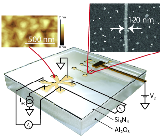
By applying a two-step temperature profile to the prepatterned substrate during the MBE growth (details provided in Methods), the SAE growth of (BiSb)2Te3 Hall-bars and nanowires is achieved. Figure 1 shows a schematic of the Al2O3 substrate with Si3N4 mask, as well as an atomic-force-microscopy (AFM) and scanning-electron-microscopy (SEM) images of the selectively-grown (BiSb)2Te3 structures. The film in the Hall-bar is continuous with triangular terraces, indicating a good epitaxy. This growth of continuous (BiSb)2Te3 is maintained even when the lateral dimensions of the exposed areas in the growth mask are constrained into nanowires as seen from the SEM image. Due to a high degree of selectivity, only a few isolated crystallites are found on the Si3N4 mask.
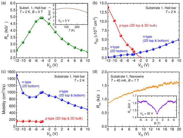
To characterise the electronic properties of the (BiSb)2Te3 film selectively-grown in the Hall-bar structure, the longitudinal sheet resistance and the Hall resistance were measured as a function of temperature , perpendicular magnetic field , and top-gate voltage . The behavior shown in the inset of Fig. 2(a) is typical for a bulk-insulating (BiSb)2Te3 film [18]. The behavior shown in the main panel of Fig. 2(a) shows a clear peak with the gate-tunabiliy of by a factor of 2, which further confirms the bulk-insulation and indicates that the chemical potential can be gate-tuned across the Dirac point of the topological surface state.
For each data point in the gating curve, we measured and as a function of the perpendicular magnetic field up to T. By employing the two-band analysis used in Refs. [23, 24, 18], we analysed the sheet carrier density and the mobility of the carriers contributing to the transport at each [see Fig. S1 in the Supporting information (SI) for the raw data] and the results are shown in Figs. 2(b) and 2(c). We identified a single -type band for V, while both - and -type carriers contribute to the transport for V. The mobility of the -type carriers is of the order of 1000 cm2/Vs which likely comes from the surface electrons in both top and bottom surfaces [18]. At V, the top surface is tuned into the -type regime where holes from both surface (2D) and bulk (3D) contribute to the transport (because of the close proximity of the bulk valence-band edge to the Dirac point of the surface state [9, 10]), while the bottom surface is still in the -type regime and keep contributing high-mobility electrons. This behavior is entirely consistent with what was reported for top-gated (BiSb)2Te3 films grown on pristine sapphire substrates [18].
While the (BiSb)2Te3 film grown in the Hall-bar structure analyzed above has shown bulk-insulation with the tunability of the chemical potential across the Dirac point, the 160-nm-wide nanowire structure grown on the very same substrate turned out to be different. Within the range of that can be applied without breaking the dielectric, the Dirac point cannot be accessed and the indicated that the nanowire was always in the -type regime [Fig. 2(d)]. This suggests that the MBE-growth condition depends on the size of the patterned features and the actual composition of (BiSb)2Te3 is different between the Hall-bar and nanowire structures, which is consistent with a past report on the SAE [12]. The lower value of the sheet resistance in the nanowire [Fig. 2(d)] compared to that in the 10-m-wide Hall-bar device on the same substrate [Fig. 2(d)] also supports this conclusion. Since this nanowire is bulk-conducting, the AB-like magnetoresistance oscillations characteristic of bulk-insulating TI nanowires [19] are not recognizable in parallel magnetic fields [see inset of Fig. 2(d) and additional data in SI].
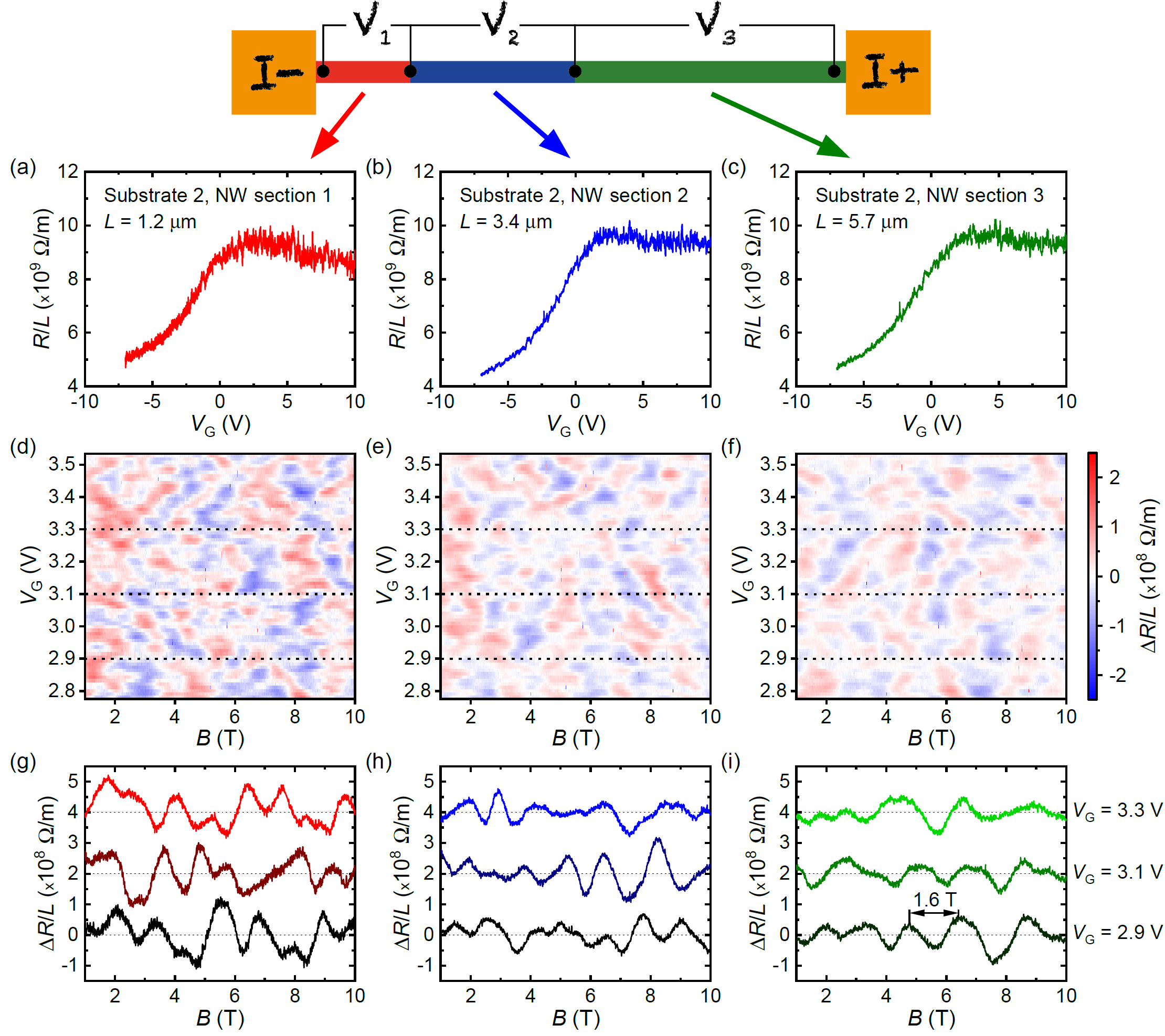
To achieve bulk-insulation in the SAE-grown nanowires, the MBE growth conditions were reoptimised for a second wafer (substrate 2), decreasing the beam-equivalent-pressure ratio of Sb/Bi from 2.1 to 1.8 (see Methods for details). For a long (BiSb)2Te3 nanowire grown on substrate 2, three sections with different lengths were investigated. Figures 3(a-b) show the -dependence of the resistance normalized by the section length for the three sections 1, 2 and 3. All three section can be tuned to the Dirac point with V and their resistances scale linearly with the wire length as expected for nanowires in the diffusive regime, demonstrating the homogeneity of the grown nanowire.
In this bulk-insulating nanowire, we observed the characteristic AB-like magnetoresistance oscillations in parallel magnetic fields stemming from the magnetic-flux-dependence of the Dirac subbands formed in TI nanowires due to the quantum size effect [19, 20, 21, 22]. The phase shift of these oscillations upon gating is commonly observed in bulk-insulating TI nanowires [21, 25, 22], and it is also the case here: After subtracting a smooth background from the raw data to obtain (see SI for details), we find oscillations whose phase shifts with [Figs. 3(d-f)]. Note that the oscillations and the phase shift have considerable irregularity, which points to strong disorder. This is understandable, because the bulk-insulation in (BiSb)2Te3 is achieved by compensation doping, which leaves charged doners and acceptors [26, 24, 27, 28, 29, 30, 31].
Interestingly, the degree to which disorder affects the regularity of flux-dependent oscillations seems to correlate with the nanowire length. While the mapping of shown in Fig. 3(d) for the shortest section is significantly disordered, a more regular pattern emerges upon increasing the wire length, as one can see in Figs. 3(e-f). One can also see this qualitative change in the individual curves of for fixed values [Figs. 3(g-i)]. This length dependence probably arises because the random resistance fluctuations due to disorder are averaged out in longer sections. In the longest 5.7-m section where the AB-like oscillations were most regular, we identify the dominant periodicity of 1.6 T, which corresponds to a cross-sectional area of m2. This value is only slightly smaller than the geometrical cross-section of the wire, m2, which was determined via AFM and SEM observations of the nanowire thickness (nm) and width (nm), respectively. The flux-relevant cross-section that is reduced from the geometrical value was previously attributed to the penetration depth of the surface-state wave function and a finite oxide shell on the surface [32, 2].
III Conclusion
We have shown that bulk-insulation can be achieved in TI structures that are SAE-grown on a patterned sapphire substrate with a Si3N4 growth mask. The high carrier mobility and the tunability of the chemical potential across the Dirac point demonstrate the suitability of this technique to engineer more complex devices. We found that the optimum growth conditions to achieve bulk-insulation changes with the feature size, but it was still possible to optimize the conditions to grow a bulk-insulating (BiSb)2Te3 nanowire with the width of only 120 nm. The AB-like magnetoresistance oscillations observed in such a nanowire confirm the quasi-1D transport through the quantum-confined topological surface state. Interestingly, our data suggest that the disorder effect, which causes random fluctuations of the wire resistance, tends to be averaged out in longer wires. The present result opens the possibility to fabricate TI-based devices to exploit various topological phenomena in a scalable manner.
IV Methods
MBE growth & device fabrication:
The SAE growth templates were created by depositing a 50-nm Si3N4 layer by hot-wire chemical vapour deposition (HW-CVD) on top of cm2 sapphire (0001) substrates. Subsequently, the growth masks were defined using electron-beam lithography, and transferred into the Si3N4 layer by reactive-ion etching with CF4. The resist was removed in acetone and isopropanol. Next, the template was exposed to a mild Ar and O2 plasma to remove any remaining resist leftovers.
The growth templates were then loaded into the MBE chamber (MBE Komponenten, Octoplus 400) and annealed up to 900∘C in ultra-high vacuum to clean off any adsorbents. Good thermal contact between the substrate and sample holder was found to be crucial for successful SAE growth, and was achieved by spot-welding all four corners of the substrate to the Mo sample holder using Ta strips. For the MBE growth of (BiSb)2Te3, high-purity Bi, Sb, and Te source materials (99.9999%, Thermo Fisher) were co-evaporated onto the substrate. For substrate 1, the beam-equivalent-pressures (BEP) for Bi, Sb, and Te were , , and mBar respectively, which yielded a bulk-insulating Hall-bar, but -type metallic nanowire. Te was supplied in excess, while Bi and Sb acted as the limiting species. The BEP ratio of Te/(Bi+Sb) was 15 and Sb/Bi was 2.1. For substrate 2, the BEP for Bi, Sb, and Te were , , and mBar [Te/(Bi+Sb) 13 and Sb/Bi 1.8], where the reduced Sb/Bi BEP ratio yielded bulk-insulating nanowires with widths in the range of nm. The substrate temperature was kept at 245∘C for the first min of the MBE deposition, during which a continuous seed layer of (BiSb)2Te3 formed on the exposed sapphire (0001) surface. Almost no nucleation of (BiSb)2Te3 crystallites occurred on the Si3N4 growth mask as the sticking coefficients for Bi, Sb, and Te at 245∘C were too low for this surface. Next, the substrate temperature was slowly increased to 285∘C in 13 min (i.e. 3∘C/min), while the deposition continued. At 285∘C the substrate was kept for an additional min in the fluxes of Bi, Sb, and Te, after which the substrate was left to cool down naturally to room temperature in zero flux. The higher growth temperature of 285∘C lead to a better morphology of the (BiSb)2Te3 film than would be obtained from growing with a constant temperature profile of 245∘C. Note, however, that a lower substrate temperature of 245∘C at the start was needed for the formation of a continuous seed layer of (BiSb)2Te3 which does not take place at 285∘C on sapphire (0001) (and Si3N4) for the Bi, Sb, and Te fluxes used in our MBE system.
Within a few minutes of taking the films out of the MBE chamber, they were capped with a 40-nm thick Al2O3 capping layer grown by atomic layer deposition (ALD) at 80∘C using Ultratec Savannah S200 to avoid degradation in air. Next, the (BiSb)2Te3 contact arms of the Hall-bar and nanowire devices were metallized by sputter-depositing 5 nm of Pt and 45 nm of Au. For this process, optical lithography was used and the Al2O3 capping layer was selectively removed in the contact areas by an aluminum etchant (Transene Type-D) heated to 50∘C. Lastly, a top-gate electrode was defined on top of the 40-nm thick Al2O3 layer by electron-beam lithography and sputter-depositing 5 nm Pt + 45 nm Au. The dimensions of the devices studied in this work are summarized in the supplement.
Measurements:
The characterization of the selectively-grown Hall-bar device (substrate 1) was carried out in a Quantum Design physical property measurement system (PPMS), which can be operated in a temperature range from K to K and in magnetic fields up to T. The measurements of the nanowire device (substrate 1) were performed in a dry dilution refrigerator (Oxford Instruments TRITON 200, base temperature 40mK) equipped with a 8-T superconducting magnet. The measurements of the magnetoresistance oscillations in the nanowire on substrate 2 were performed in a 3He cryostat (Oxford Instrument Heliox) at a base temperature of mK in magnetic fields up to T. The nanowire (Hall-bar) devices were measured using standard lock-in techniques in a four-terminal configuration with an ac excitation current of nA (A) and a lock-in frequency of Hz.
Data and materials availability:
Raw data used in the generation of main and supplementary figures are available in Zenodo with the identifier 10.5281/zenodo.10964435.
V Acknowledgements
We would like to thank Ella Nikodem, Cornelius Dietrich, and Sandra Omoragbon for the technical support in creating the SAE growth templates. This work has received funding from the Deutsche Forschungsgemeinschaft (DFG, German Research Foundation) under CRC 1238-277146847 (subprojects A04 and B01) and also from the DFG under Germany’s Excellence Strategy – Cluster of Excellence Matter and Light for Quantum Computing (ML4Q) EXC 2004/1-390534769, as well as from the DFG Project No. 398945897.
References
- Breunig and Ando [2022] Breunig, O.; Ando, Y. Opportunities in topological insulator devices. Nat. Rev. Phys. 2022, 4, 184–193.
- Rosenbach et al. [2020] Rosenbach, D.; Oellers, N.; Jalil, A. R.; Mikulics, M.; Kölzer, J.; Zimmermann, E.; Mussler, G.; Bunte, S.; Grützmacher, D.; Lüth, H.; Schäpers, T. Quantum Transport in Topological Surface States of Selectively Grown Bi2Te3 Nanoribbons. Advanced Electronic Materials 2020, 6, 2000205.
- Rosenbach et al. [2022] Rosenbach, D.; Moors, K.; Jalil, A. R.; Kölzer, J.; Zimmermann, E.; Schubert, J.; Karimzadah, S.; Mussler, G.; Schüffelgen, P.; Grützmacher, D.; Lüth, H.; Schäpers, T. Gate-induced decoupling of surface and bulk state properties in selectively-deposited Bi2Te3 nanoribbons. SciPost Phys. Core 2022, 5, 017.
- Kölzer et al. [2021] Kölzer, J.; Moors, K.; Jalil, A. R.; Zimmermann, E.; Rosenbach, D.; Kibkalo, L.; Schüffelgen, P.; Mussler, G.; Grützmacher, D.; Schmidt, T. L.; Lüth, H.; Schäpers, T. In-plane magnetic field-driven symmetry breaking in topological insulator-based three-terminal junctions. Communications Materials 2021, 2, 116.
- Behner et al. [2023] Behner, G.; Jalil, A. R.; Heffels, D.; Kölzer, J.; Moors, K.; Mertens, J.; Zimmermann, E.; Mussler, G.; Schüffelgen, P.; Lüth, H.; Grützmacher, D.; Schäpers, T. Aharonov-Bohm Interference and Phase-Coherent Surface-State Transport in Topological Insulator Rings. Nano Letters 2023, 23, 6347–6353.
- Schüffelgen et al. [2019] Schüffelgen, P. et al. Selective area growth and stencil lithography for in situ fabricated quantum devices. Nature Nanotechnology 2019, 14, 825–831.
- Kölzer et al. [2023] Kölzer, J.; Jalil, A. R.; Rosenbach, D.; Arndt, L.; Mussler, G.; Schüffelgen, P.; Grützmacher, D.; Lüth, H.; Schäpers, T. Supercurrent in Bi4Te3 Topological Material-Based Three-Terminal Junctions. Nanomaterials 2023, 13, 293.
- Schmitt et al. [2022] Schmitt, T. W. et al. Integration of Topological Insulator Josephson Junctions in Superconducting Qubit Circuits. Nano Letters 2022, 22, 2595–2602.
- Kong et al. [2011] Kong, D.; Chen, Y.; Cha, J. J.; Zhang, Q.; Analytis, J. G.; Lai, K.; Liu, Z.; Hong, S. S.; Koski, K. J.; Mo, S.-K.; Hussain, Z.; Fisher, I. R.; Shen, Z.-X.; Cui, Y. Ambipolar field effect in the ternary topological insulator (BixSb1-x)2Te3 by composition tuning. Nat. Nanotechnol. 2011, 6, 705–709.
- Zhang et al. [2011] Zhang, J.; Chang, C.-Z.; Zhang, Z.; Wen, J.; Feng, X.; Li, K.; Liu, M.; He, K.; Wang, L.; Chen, X.; Xue, Q.-K.; Ma, X.; Wang, Y. Band structure engineering in (Bi1-xSbx)2Te3 ternary topological insulators. Nat. Commun. 2011, 2, 574.
- Lanius [2018] Lanius, M. Topological Insulating Tellurides: How to tune Doping, Topology, and Dimensionality. Ph.D. thesis, RWTH Aachen University, 2018.
- Jalil et al. [2023] Jalil, A. R.; Schüffelgen, P.; Valencia, H.; Schleenvoigt, M.; Ringkamp, C.; Mussler, G.; Luysberg, M.; Mayer, J.; Grützmacher, D. Selective Area Epitaxy of Quasi-1-Dimensional Topological Nanostructures and Networks. Nanomaterials 2023, 13, 354.
- Park et al. [2012] Park, J.; Soh, Y.-A.; Aeppli, G.; Bland, S. R.; Zhu, X.-G.; Chen, X.; Xue, Q.-K.; Grey, F. Crystal structure and epitaxy of Bi2Te3 films grown on Si. Appl. Phys. Lett. 2012, 101, 221910.
- Richardson et al. [2017] Richardson, C. L.; Devine-Stoneman, J. M.; Divitini, G.; Vickers, M. E.; Chang, C.-Z.; Amado, M.; Moodera, J. S.; Robinson, J. W. A. Structural properties of thin-film ferromagnetic topological insulators. Sci. Rep. 2017, 7, 12061.
- Lanius et al. [2016] Lanius, M.; Kampmeier, J.; Weyrich, C.; Kölling, S.; Schall, M.; Schüffelgen, P.; Neumann, E.; Luysberg, M.; Mussler, G.; Koenraad, P. M.; Schäpers, T.; Grützmacher, D. P-N junctions in ultrathin topological insulator Sb2Te3/Bi2Te3 heterostructures grown by molecular beam epitaxy. Cryst. Growth Des. 2016, 16.
- Fu and Kane [2008] Fu, L.; Kane, C. L. Superconducting proximity effect and Majorana fermions at the surface of a topological insulator. Phys. Rev. Lett. 2008, 100, 096407.
- Legg et al. [2021] Legg, H. F.; Loss, D.; Klinovaja, J. Majorana bound states in topological insulators without a vortex. Phys. Rev. B 2021, 104, 165405.
- Yang et al. [2015] Yang, F.; Taskin, A. A.; Sasaki, S.; Segawa, K.; Ohno, Y.; Matsumoto, K.; Ando, Y. Dual-Gated Topological Insulator Thin-Film Device for Efficient Fermi-Level Tuning. ACS Nano 2015, 9, 4050–4055.
- Peng et al. [2010] Peng, H.; Lai, K.; Kong, D.; Meister, S.; Chen, Y.; Qi, X.-L.; Zhang, S.-C.; Shen, Z.-X.; Cui, Y. Aharonov–Bohm interference in topological insulator nanoribbons. Nature Materials 2010, 9, 225–229.
- Xiu et al. [2011] Xiu, F.; He, L.; Wang, Y.; Cheng, L.; Chang, L.-T.; Lang, M.; Huang, G.; Kou, X.; Zhou, Y.; Jiang, X.; Chen, Z.; Zou, J.; Shailos, A.; Wang, K. L. Manipulating surface states in topological insulator nanoribbons. Nature Nanotechnology 2011, 6, 216–221.
- Cho et al. [2015] Cho, S.; Dellabetta, B.; Zhong, R.; Schneeloch, J.; Liu, T.; Gu, G.; Gilbert, M. J.; Mason, N. Aharonov–Bohm oscillations in a quasi-ballistic three-dimensional topological insulator nanowire. Nature Communications 2015, 6, 7634.
- Rößler et al. [2023] Rößler, M.; Fan, D.; Münning, F.; Legg, H. F.; Bliesener, A.; Lippertz, G.; Uday, A.; Yazdanpanah, R.; Feng, J.; Taskin, A.; Ando, Y. Top-Down Fabrication of Bulk-Insulating Topological Insulator Nanowires for Quantum Devices. Nano Letters 2023, 23, 2846–2853.
- Ren et al. [2010] Ren, Z.; Taskin, A. A.; Sasaki, S.; Segawa, K.; Ando, Y. Large bulk resistivity and surface quantum oscillations in the topological insulator Bi2Te2Se. Phys. Rev. B 2010, 82, 241306.
- Ando [2013] Ando, Y. Topological Insulator Materials. J. Phys. Soc. Jpn. 2013, 82, 102001.
- Kim et al. [2020] Kim, H.-S.; Hwang, T.-H.; Kim, N.-H.; Hou, Y.; Yu, D.; Sim, H.-S.; Doh, Y.-J. Adjustable Quantum Interference Oscillations in Sb-Doped Bi2Se3 Topological Insulator Nanoribbons. ACS Nano 2020, 14, 14118–14125.
- Skinner et al. [2012] Skinner, B.; Chen, T.; Shklovskii, B. I. Why Is the Bulk Resistivity of Topological Insulators So Small? Phys. Rev. Lett. 2012, 109, 176801.
- Borgwardt et al. [2016] Borgwardt, N.; Lux, J.; Vergara, I.; Wang, Z.; Taskin, A. A.; Segawa, K.; van Loosdrecht, P. H. M.; Ando, Y.; Rosch, A.; Grüninger, M. Self-organized charge puddles in a three-dimensional topological material. Phys. Rev. B 2016, 93, 245149.
- Knispel et al. [2017] Knispel, T.; Jolie, W.; Borgwardt, N.; Lux, J.; Wang, Z.; Ando, Y.; Rosch, A.; Michely, T.; Grüninger, M. Charge puddles in the bulk and on the surface of the topological insulator studied by scanning tunneling microscopy and optical spectroscopy. Phys. Rev. B 2017, 96, 195135.
- Breunig et al. [2017] Breunig, O.; Wang, Z.; Taskin, A.; Lux, J.; Rosch, A.; Ando, Y. Gigantic negative magnetoresistance in the bulk of a disordered topological insulator. Nat. Commun. 2017, 8, 15545.
- Nandi et al. [2018] Nandi, D.; Skinner, B.; Lee, G. H.; Huang, K.-F.; Shain, K.; Chang, C.-Z.; Ou, Y.; Lee, S.-P.; Ward, J.; Moodera, J. S.; Kim, P.; Halperin, B. I.; Yacoby, A. Signatures of long-range-correlated disorder in the magnetotransport of ultrathin topological insulators. Phys. Rev. B 2018, 98, 214203.
- Lippertz et al. [2022] Lippertz, G.; Bliesener, A.; Uday, A.; Pereira, L. M. C.; Taskin, A. A.; Ando, Y. Current-induced breakdown of the quantum anomalous Hall effect. Phys. Rev. B 2022, 106, 045419.
- Zhang and Vishwanath [2010] Zhang, Y.; Vishwanath, A. Anomalous Aharonov-Bohm Conductance Oscillations from Topological Insulator Surface States. Phys. Rev. Lett. 2010, 105, 206601.