Point defects in CdTe and CdTeSe alloy: a first principles investigation with DFT+U
Abstract
CdTe and its alloy CdTeSe are widely used in optoelectronic devices, such as radiation detectors and solar cells, due to their superior electrical properties. However, the formation of defects and defect complexes in these materials can significantly affect their performance. As a result, understanding the defect formation and recombination processes in CdTe and CdTeSe alloy is of great importance. In recent years, density functional theory (DFT) calculations have emerged as a powerful tool for investigating the properties of defects in semiconductors. In this paper, we use DFT+U calculations to comprehensively study the properties of intrinsic defects as well as extrinsic defects induced by commonly used dopants, such as Cu and group V elements, in CdTe and CdTeSe alloy. This work provides insights into the effects of these defects on the electrical and optical properties of the material.
I Introduction
Cadmium telluride (CdTe) and its alloy with selenium (CdTeSe) have been extensively studied due to their high potential for use in optoelectronic devices, including solar cells and radiation detectors. Compared to CdTe, the addition of Se to the alloy has been shown to improve the material’s electronic properties, such as its bandgap and carrier mobility, making it a promising candidate for high-efficiency solar cell applications [1]. The performance of these devices, however, can be significantly impacted by the presence of point defects, which can affect the material’s electrical and optical properties. To better understand the effects of defects on the properties of CdTeSe, it is necessary to investigate the formation and recombination of defects and defect complexes in this material. In this work, we use density functional theory (DFT) calculations to investigate the properties of intrinsic defects, copper and group V dopants in CdTeSe, with a focus on the formation of point defects and their impact on the material’s electronic properties.
II Methods
II.1 FIRST-PRINCIPLES CALCULATION METHODS
Most DFT calculations apply the generalized gradient approximation (GGA) or local density approximation (LDA) as the exchange-correlation functional. However, it is widely known that DFT with LDA or GGA is likely to underestimate the bandgap of semiconductors. For CdTe, GGA gives us a bandgap of 0.68 eV, which is much smaller than experimental values ( 1.5 eV). This can be explained by the overestimation of the delocalization of Cd-4 electrons, which lifts the valence electron energies (the Te-5 valence band) [2]. There are many approaches to correct the exchange-correlation functional, such as self-interaction correction (SIC) calculations, hybrid functional of Heyd, Scuseria and Ernzerhof (HSE) and spin-orbit coupling (SOC). However, these methods are computationally expensive, which makes them impractical for study of defects in alloys due to the massive number of possible configurations. DFT with coulomb self-interaction potentials (GGA+U) is another method that has been frequently used to correct the calculated bandgaps [2]. This method combines Hubbard-like model for a portion of states in the system with Coulomb self-interaction potentials (U) to select bands for correction. Non-integer or double occupations of states are described by introducing of two parameters: (1) U, which reflects the intensity of the on-site Coulomb interaction, and (2) J, which adjusts the intensity of the exchange interaction. Typically, for simplicity, an effective parameter Ueff U J is used. This effective parameter Ueff is typically referred to as U.
II.2 Computational Details
Our investigation reveals that setting U=12.2 eV[3] for Cd-4 orbitals in CdTe closely matches the experimental lattice constant and bandgap, showcasing the effectiveness of the GGA+U method. In comparison, while the HSE method accurately reproduces the experimental bandgap, it tends to overestimate lattice constants, indicating a larger error margin compared to the GGA+U approach.
Applying the optimized U parameter to zinc blende and wurtzite structures of CdSe, we observe a surprisingly good agreement with experimental data, surpassing the performance of the HSE06 hybrid method. Specifically, the bandgap and lattice parameters of zinc blende CdSe align closely with experimental results, as detailed in Table 1. For the wurtzite structure, although GGA+U slightly underestimates lattice parameters, the bandgap predictions remain consistent.
This consistent accuracy across both CdTe and CdSe can be attributed to the similar - coupling inherent to Cd-Te and Cd-Se bonds, with both Te and Se being group VI elements. The GGA+U method effectively lowers the Cd 4 bands, enhancing - coupling. With U=12.2 eV, it provides a suitable correction for both materials.
Leveraging this optimized U value, we extend our study to the full composition range of the CdTeSe alloy. A notable advantage of the GGA+U method is its lower computational cost compared to HSE06, facilitating the application to supercells of the CdTeSe alloy with varied Se/Te arrangements and defect calculations. This approach also allows for the extension to larger supercells at a manageable computational expense when some defect calculations yield less reliable results due to elastic error[4].
Structural optimizations and energy calculations were carried out using the VASP code. For the GGA+U calculations, we employed the Perdew, Burke, and Ernzerhof (PBE) exchange-correlation functional. Additionally, the HSE06 functional with default parameters was utilized for comparative analysis. The calculations were performed with a plane wave cutoff energy of 450 eV for the wave functions. The Brillouin zones for all structures under investigation were sampled using -centered k-point grids. Specifically, a 222 k-point grid was employed for both 64-atom and 216-atom supercells, while a 111 grid was applied to the 512-atom supercell.
In the study of CdTeSe alloy, we focus on compositions of CdTe0.75Se0.25 and CdTe0.50Se0.50. This selection is informed by the fact that the cubic phase of CdTe1-xSex is stable for [5]. In contrast, the hexagonal phase (wurtzite structure) of CdTe1-xSex emerges for , which is not considered to be photoactive[6, 5]. Moreover, in most state-of-the-art CdTeSe technologies, the Se ratio typically remains below 40%[7, 1, 8]. Consequently, we will not extend our study to higher Se ratios.
Utilizing a supercell program[9], we generate 20 configurations for each alloy composition, prioritizing those with the highest frequency of occurrence. The configuration selected as the reference structure is the one whose formation energy is closest to the Boltzmann distribution average of the formation energies for all configurations sharing the same alloy ratio. This reference supercell then serves as the basis for generating defect supercells. In addressing defects within the alloy, we examine multiple configurations that exhibit varying Se/Te arrangement environments. For these defects, we opt for the Boltzmann distribution average at 873 K as a representative formation energy values across at least four configurations for each point defect.
Method GGA+U HSE06 Experiment[10] Bandgap (eV) (Å) Bandgap (eV) (Å) Bandgap (eV) (Å) CdTe (Zinc Blende) 1.50 6.46 1.50 6.58 1.50 6.48 CdSe (Zinc Blende) 1.72 5.95 - - 1.71 5.98 CdSe (Wurtzite) 1.79 1.68 1.80
The defect formation energy can be derived from DFT using the supercell method[11] by the following equation,
| (1) |
where is the formation energy of a defect , is the total energy of one defect state with charge , is the total energy of a bulk unit cell with the same size of the defected cell, and is the reference energy of added/removed atoms of an element at given chemical potential . For any defects in this paper, the chemical potentials of all species are defined with reference to the elemental standard states. is the valence band maximum as computed from electronic structure of bulk supercell.
is the charge correction energy to account for interaction between periodic images. The conventional FNV correction method[12] exhibits a tendency for overestimating or underestimating the charge correction, especially when dealing with partially or fully delocalized defects[13]. In order to address this issue and enhance the accuracy of the correction process, a strategic modification is implemented. Instead of directly applying the FNV correction to these complex defects, we choose to initiate the correction process by employing the density derived electrostatic and chemical (DDEC) method to determine the net atomic charges (NACs)[14, 15, 16]. This preliminary step serves the purpose of precisely ascertaining the charge localization within the system.
Following the DDEC analysis, the of the defects are determined. To find out the unscreened localized charge used in FNV correction, a scaling factor is introduced. This scaling factor is carefully calibrated to reintroduce the screening effect that may be lost during the charge localization process. Subsequently, , scaled by the aforementioned factor , is treated as the input localized charge for the FNV charge correction method,
| (2) |
The factor can be determined using one of two approaches. The first approach involves selecting defects that are fully localized; in this scenario, the nominal charge of the defects is equal to , facilitating straightforward determination of . However, this method may not always be feasible due to the prerequisite knowledge required about defect localization. Alternatively, the second approach entails adjusting the supercell size and iteratively testing values to achieve convergence in the defect formation energies across varying supercell dimensions. For both strategies, it is advisable to select defects with substantial values, as this can lead to significant correction values. Such a selection ensures the derived values are both reasonable and effective.
In this study, we select as the reference defect due to its advantageous properties. Specifically, the Kohn-Sham level of is located within the band gap, and it exhibits a large capture cross section for both the (0/+1) and (+1/+2) transitions, as discussed in Sec. III.1 and corroborated by existing literature[17]. We firstly apply first approach to determine universal value of 3.5 for CdTe, CdTe0.75Se0.25, and CdTe0.50Se0.50. This value is then verified by the second approach by increasing supercell size.
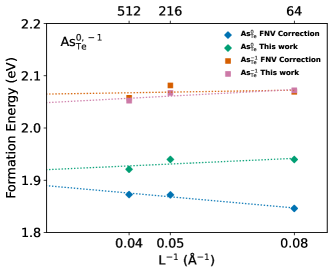
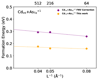
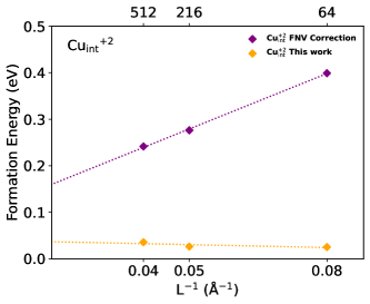
Figure 1 showcases the effectiveness of our charge correction method in overcoming the limitations associated with the FNV correction approach. Our method notably addresses several critical issues:
-
•
Non-zero NACs in neutral defects, such as illustrated in Fig. 1a, result in image interactions that necessitate charge correction, a scenario not accommodated by FNV correction. Our method’s application of charge correction to these defects is supported by improved convergence, as evident in Fig. 1a. For instance, the transition level for (0/-1) shifts from 0.22 eV without charge correction to 0.13 eV with it, more closely aligning with experimental ( meV) [18] and hydrogenic model predictions ( meV) [19]. Similarly, the transition level for (0-1) improves from 0.16 eV to 0.11 eV, nearing experimental values ( meV) [18].
-
•
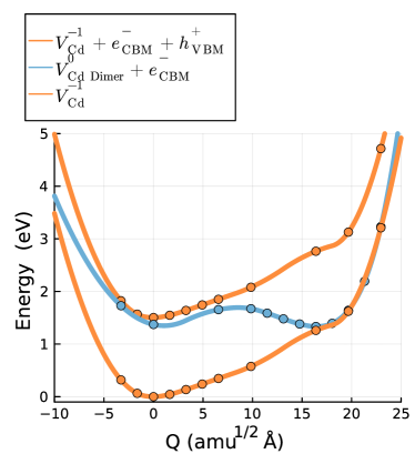
For charged defects that are not fully localized, our method accurately accounts for the discrepancy between localized charge and nominal charge, avoiding the overcorrection observed with FNV correction. This accuracy is validated by the consistent formation energy results for across supercells of 64, 216, and 512 atoms, as shown in Fig. 1c.
-
•
Additionally, our approach adeptly determines the localized charge distribution of complex defects, a task for which FNV correction’s charge assignment proves ambiguous and results in poor convergence. Our method’s ability to assign to specific defect positions leads to improved convergence for complex defects such as , as demonstrated in Fig. 1b.
These findings highlight the comprehensive capabilities of our charge correction method in accurately modeling defect properties, surpassing the limitations of existing approaches.
III Results and Discussion
III.1 Intrinsic Defects

The cadmium vacancy is a pivotal intrinsic defect in CdTe and its alloys, with its configuration and transition levels being subjects of significant debate in both theoretical and experimental literature[20]. Our research reveals that the neutral state of primarily adopts symmetry, featuring two fully occupied degenerate states and one unoccupied state. In contrast, the -1 and -2 charged states are most stable in symmetry. The transition levels of , as established in various studies, range from 0.1 to 0.8 eV above the VBM [21, 22, 23, 24, 25, 26, 27]. In this work, the transition levels for in CdTe are identified as 0.17 eV for the (-1/0) transition and 0.30 eV for the (-2/-1) transition. For CdTe0.75Se0.25, these levels are 0.16 eV and 0.30 eV, respectively, while for CdTe0.50Se0.50 they are 0.14 eV and 0.35 eV, respectively. These findings indicate that the transition levels of exhibit relative consistency in alloys with a selenium ratio below 50%.
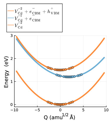
Furthermore, we calculated the defect capture cross section of in CdTe based on static approximation[28, 11, 29, 30, 31, 32]. The results, presented in Fig. 3 and Table 2, reveal that the potential energy surface (PES) of the (-2/-1) transition is quasi-harmonic, while the PES of the (-1/0) transition is anharmonic. This discrepancy can be attributed to the proximity of metastable and states, which merge with the most stable configurations of these respective charge states—a phenomenon also observed elsewhere in HSE06 calculation of [33] and defects in GaAs[32]. From the carrier capture cross section calculations, we determined that the (-1/0) transition exhibits strong nonradiative recombination intensity, whereas the (-2/-1) transition demonstrates only weak nonradiative recombination. This observation aligns with previous reports using the HSE06 functional[33, 17].
| Defect | Transition Level | Trapping Process | |
| (-2/-1) | hole capture | ||
| electron capture | |||
| (-1/0) | hole capture | ||
| electron capture | |||
| (+2/+1) | hole capture | ||
| electron capture | |||
| (+1/0) | hole capture | ||
| electron capture |
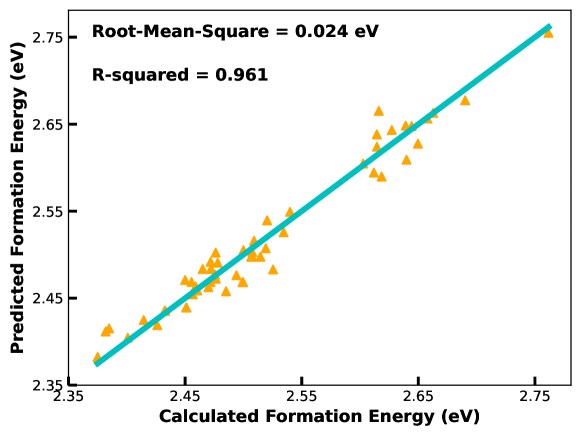
The second critical intrinsic defect under investigation is . The charge states and both exhibit symmetry as shown in Fig. 4, while displays symmetry. A significant dependence on the Se/Te arrangement is observed for defects with symmetry. To exemplify this, we considered and calculated its formation energy for 56 different local Se/Te environments. We employed a neighbor counting linear regression model, as detailed in Table 3, which effectively captures this dependence using eight features. The fitting results, illustrated in Fig. 5, demonstrate the model’s accuracy.
The eight features considered in the model include the Se ratio, Se ratio square, the presence of a first nearest neighbor (1NN) Se atom with a long bond, the count of 1NN Se atoms with short bonds, the square of the count of 1NN Se atoms with short bonds, the presence of second nearest neighbors (2NN) with one long and one short bond, 2NN with one long bond, and 2NN with one short bond. The positive coefficients for the Se ratio and Se ratio square suggest that higher Se ratios make the formation of less favorable. The feature 1NN Se with a long bond indicates whether the elongated bond in the configuration is occupied by Se, with its negative coefficient implying that the presence of Se in this bond promotes defect formation. The features 1NN Se with short bonds and its square capture a quadratic relationship between the formation energy of defects and the occupancy of short bonds by Se, with the minimum of the quadratic function occurring near a Se ratio of 0.8. This indicates a decrease in formation energy as more Se atoms occupy the 1NN short bonds with Se ratio less than 80 %. The final three features account for the 2NN Se/Te atoms and whether they are neighbors to the 1NN with elongated or short bond, or both. The positive coefficient for 2NN (1 Long, 1 Short) and negative coefficients for both 2NN (1 Long) and 2NN (1 Short) reflect the diverse preferences for the defect configuration. This model can be further integrated with Lattice Monte Carlo simulations to elucidate the impact of the local environment on . Additionally, we performed calculations for the capture cross section of this defect, with results presented in Table 2. These findings validate that can create deep-level trap centers, aligning with previous HSE06 calculations and experimental observations[17, 34].
Feature (eV) Feature (eV) Se ratio (1NN Se with short bonds)2 (Se ratio)2 2NN (1 Long, 1 Short) 1NN Se with long bond 2NN (1 Long) 1NN Se with short bonds 2NN (1 Short)
The defects , , and are identified as shallow donors, exhibiting several common characteristics. Both and display negative-U behavior. The (+2/0) transition states of and , along with the (+2/+1) transition state of , are situated near the conduction band minimum (CBM) or embedded within the conduction band (CB). Consequently, the +2 charge state is predominant for all three defects in -type CdTe and its alloys. Only minor variations in their formation energies are observed with Se alloying, suggesting that these defects will continue to act as compensating defects in intrinsic CdTeSe alloys. Among these, exhibits the highest formation energy under both Cd-rich and Te-rich conditions, indicating that it is unlikely to be the dominant compensating defect. The neutral state of is most stable in a Jahn-Teller distorted structure, consistent with HSE06 calculations[20]. The state is most stable in symmetry, while is most stable when positioned in a tetrahedral vacant site surrounded by four group VI atoms.
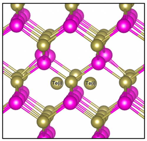
Interstitial tellurium is identified as a donor. We used ab-initio molecular dynamics (MD) to run simulated annealing, a technique for finding global energy minimums of without an initial guess structure. Essentially, the system begins at high temperature and is slowly cooled, eventually settling into a low energy configuration. MD was run in the canonical (NVT) ensemble, using the Nose-Hoover thermostat to control the system temperature. The system was advanced with a 6 femtosecond time step for 1000 steps, starting at 1000K and ending at 1K. We found prefers to form split interstitial oriented along the [110] directions. Ref. [35] find identical stable configurations. Some studies suggest that could be a deep-level defect[17, 34], and our findings indicate that the transition level of is indeed located near the mid-gap. However, the formation energy of is not particularly favorable, even under Te-rich conditions. Based on its formation energy and our compositionally constrained thermodynamic (CCT) method[36], we estimate that the density of at 300K is around three orders of magnitude lower than the carrier density and the densities of two other deep-level defects, and , under Te-rich condition. Consequently, the effectiveness of in limiting carrier lifetime is questionable. This aspect will be further explored in our future work.
The defect can potentially form complexes with and due to strong binding energy[37]. We have investigated the formation energies of the and complexes in Fig. 2 and employed the CCT to estimate their densities. However, the results are similar to those for . We determined that the density of these two complexes at 300 K is approximately three orders of magnitude lower than the carrier density. Further investigation is required to ascertain whether these complexes significantly impact the defect distribution.
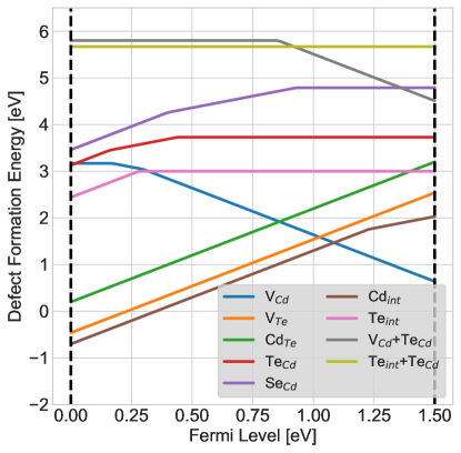
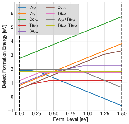
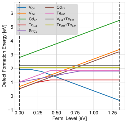
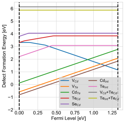
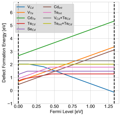
We have also explored dominant deep level defect formation energy in CdTeSe alloy with varied Se/Te ratio. Dominant defect formation energy in CdTe and CdTeSe for different charge states are depicted in Fig. 2. It is clearly observable that deep level defects have higher formation energy in Cd-rich condition. In fact, both experimental observation and HSE06 results validate this observation that as CdTe becomes more Cd-rich, a longer minority carrier lifetime can be achieved[34]. This conclusion remains valid in CdTeSe alloy. Moreover, from experiment observation[38, 39], the bulk recombination in CdTeSe alloy is lowered in CdTe. Fig. 2 shows that the formation energy of deep level defects ( and ) slightly increases as we raise the Se ratio. Specifically, The of is 0.15 eV higher in 50% alloy while of is 0.18 eV higher. This suggests a lower density of deep level centers in CdTeSe alloy. In addition, Se alloying could possibly deactivate the recombination centres by forming Se-complexes[39]. Thus, it is expected that bulk recombination will be reduced in CdTeSe alloy.
Examination of Fig. 2b, Fig. 2d, and Fig. 2f reveals that the Fermi level is consistently pinned around 0.6 eV across CdTe, CdTe0.75Se0.25, CdTe0.50Se0.50 compositions for Te-rich condition. Under such condition, the dominant acceptor is and the dominant compensating donors are , , and . For Cd-rich condition, is observed to be pinned between 1.2 eV and 1.3 eV for the same compositions. Under such condition, the dominant acceptor is and the dominant compensating donors are , and . These findings align closely with Yang’s first-principles calculations using the HSE06 functional[20], highlighting the intrinsic self-doping limits under equilibrium growth conditions. Interestingly, this limitation may potentially be circumvented by employing rapid cooling from high temperatures[20]. Nonetheless, the current method for calculating defect formation energies in the alloy, utilizing a Boltzmann distribution average at 873 K, simplifies the analysis but might not adequately address the intricacies arising from defects significantly influenced by the Se/Te arrangement. In addition, defect interaction is omitted when the material is cooling down from high temperature. Achieving a more detailed defect profile necessitates the integration of Lattice Monte Carlo simulations and continuum simulations[40, 41, 42]. These advanced simulation techniques are planned for inclusion in our future work, promising a deeper understanding of defect dynamics within the alloy.
III.2 Group V Dopants
Arsenic (As) and phosphorus (P) have been identified as effective dopants in CdTe-based materials, offering potential for enhancing p-type doping in solar cells[43]. However, the behavior of As and P in CdTeSe, such as the primary sources of compensating defects in As- and P-doped CdTe, remains less understood[44].
As anticipated, As can substitute for Te or Se in CdTeSe, acting as an acceptor due to its group V nature, possessing one electron fewer than Te. In this study, we focus on the substitutional defect and , as other related defects, like As/P interstitials, exhibit relatively higher formation energies[43]. Our calculations show that the neutral and -1 charged states of and display symmetry, consistent with previous reports[43]. The calculated (0/-1) transition levels for and are 0.13 eV and 0.18 eV, respectively (Table 4, Table 5), indicating shallow levels suitable for -type CdTe doping. However, the transition level of shifts toward the CBM, reaching 0.31 eV above the valence band maximum (VBM) when the Se ratio is 50%. Conversely, the transition level of remains close to the VBM even as the Se ratio increases. This suggests that for As-doped CdTeSe, careful control of the Se ratio is necessary to maintain reasonable As doping efficiency.
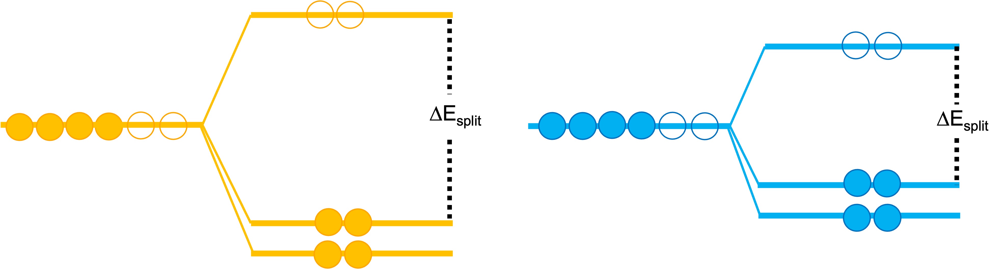
Furthermore, As and P can form a +1 charged AX center defect, converting it into a donor[43, 45]. As depicted in Fig. 7, this asymmetric defect occurs when As/P shifts toward one of the neighboring Te atoms, causing the triply degenerate state to split into two fully occupied states and one empty state, as illustrated in Fig. 8. This process results in the breaking of one bond with a neighboring Cd atom for each of the two atoms. If the band splitting energy exceeds the bonding energy with Cd, the AX defect becomes more stable than the tetrahedral As/P substitutional defect. However, our calculations indicate that in CdTe the formation energy of the As AX center is 1.92 eV, similar to that of at 1.93 eV. Similarly, the P AX center has a formation energy of 2.04 eV, close to at 2.10 eV, suggesting that the AX center does not provide additional stability.
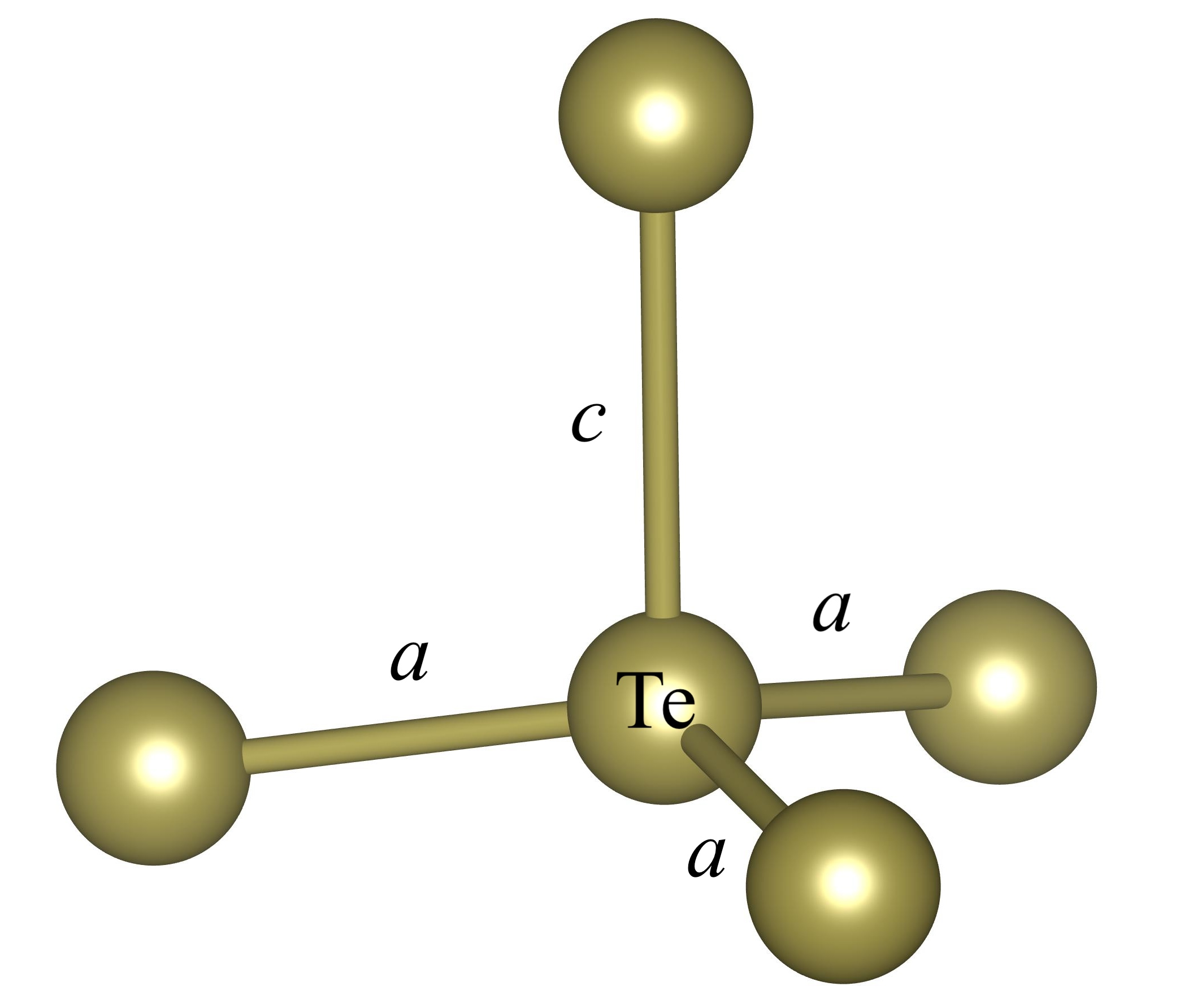
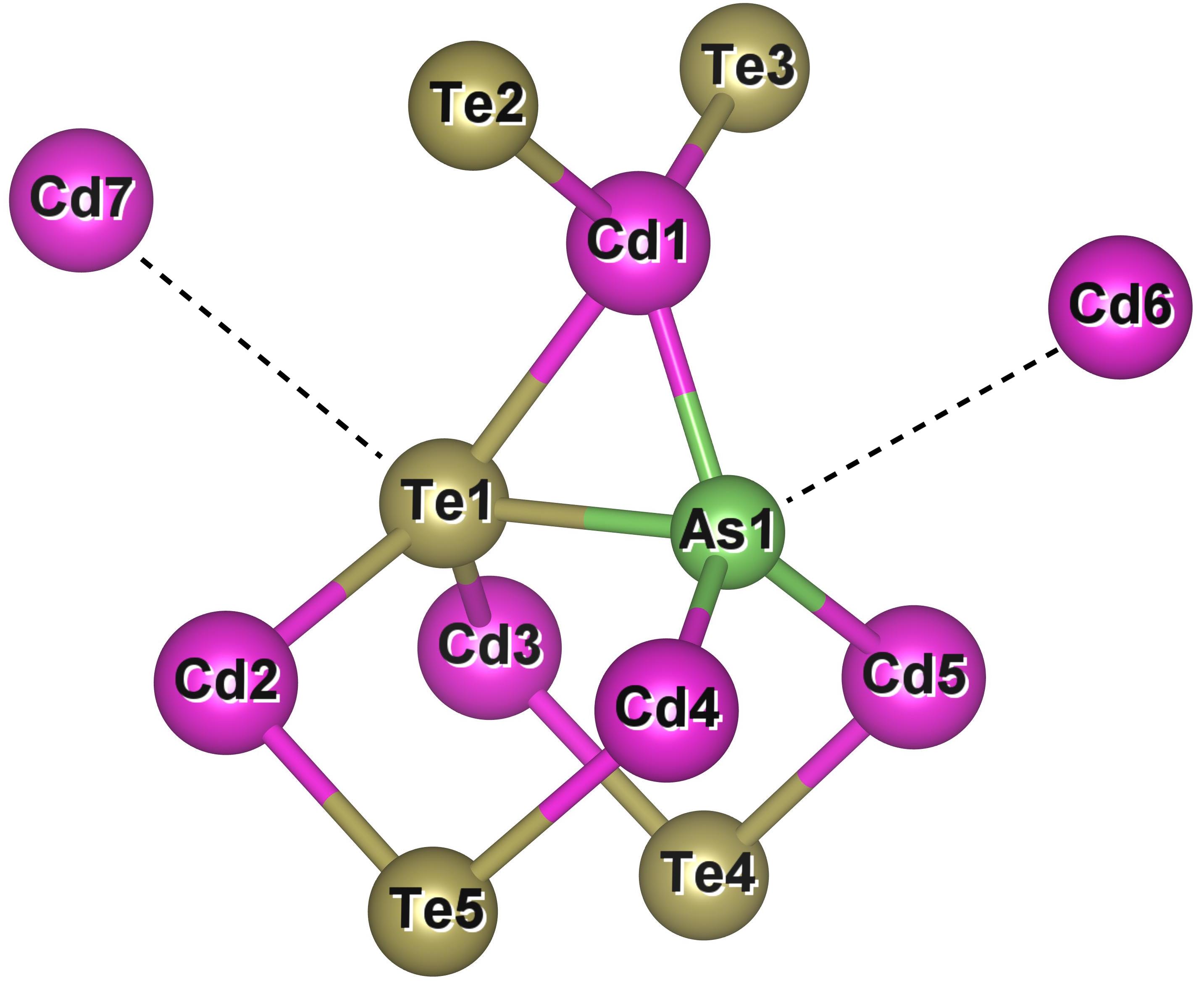
As the Se ratio increases, the +1 charge state of exhibits a formation energy of 1.93 eV in CdTe, 1.89 eV in CdTe0.75Se0.25, and 1.84 eV in CdTe0.50Se0.50, indicating a slight preference for the +1 defect with higher Se alloying. However, the formation energy of the AX defect significantly decreases with increasing Se ratio in the CdTeSe alloy. For instance, in CdTe0.75Se0.25, the formation energy of the AX defect ranges from 1.57 eV to 1.79 eV for different Se/Te arrangements, compared to 1.92 eV in CdTe. This suggests a possible interaction between Se and the AX defect that could lower the formation energy of the AX defect and compensate for p-type doping. As shown in Fig. 8, the favorable formation energy of the AX defect is not attributed to an increase in , but rather to the nearby Se atom potentially weakening the bond between Cd and As/Te. In fact, our study of a 64-atom supercell of CdTeSe alloy with only one Se atom in the group VI lattice revealed that the lowest formation energy of the AX defect occurred when either the Te4 or Te5 atom was replaced with a Se atom. From Fig. 7, it can be inferred that when a smaller Se atom is placed into positions Te4 and Te5, the nearby Cd atoms are compressed in the direction of As1-Te1, strengthening the As1-Te1 bond but weakening the As1-Cd6 and Te1-Cd7 bonds. Moreover, we observed that the As atom tends to move toward the Te atom to form a dimer structure in the alloy, while moving toward the Se atom is not energetically favorable. A similar behavior is observed for as well.
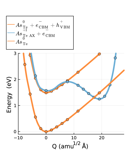
To further unveil the impact of AX center defects on group V dopability, we explore the transition mechanism between the AX center defect and the neutral substitutional defect within a 25% CdTeSe alloy. We plot the configuration coordinate diagram (CCD) of (+1_AX/0) in Fig. 9a. The significant barrier ( eV) between the AX and states likely limits the occurrence of AX defects, a finding consistent with similar transition barriers reported in CdTe[45]. Although certain alloy arrangements may promote AX defect formation, the overall quantity of AX defects may still be limited, due to the notable transition barrier between the AX defect and the positively charged defect. Recent computational findings[44] indicate that AX centers do not constitute a bottleneck for p-type doping in CdTe and CdTeSe alloys. Therefore, the significance of AX centers on the dopability of group V elements requires further investigation, taking into account both the kinetic and thermodynamic aspects of AX defect formation.
AX (-1/0) CdTe 1.92 1.93 1.94 2.07 0.13 0.16 2.34 CdTe0.25Se0.75 1.571.79 1.89 1.93 2.11 0.18 0.09 2.42 CdTe0.50Se0.50 1.701.87 1.84 1.87 2.19 0.31 0.06 2.42
AX (-1/0) CdTe 2.04 2.10 1.93 2.04 0.11 0.20 2.51 CdTe0.25Se0.75 1.721.94 2.08 2.05 2.09 0.04 0.08 2.46 CdTe0.50Se0.50 1.822.01 2.10 2.07 2.13 0.06 0.05 2.45
A remaining question is the identity of the dominant compensating donor. Chatratin 2023[44] suggests that or could be potential compensating donors, but they exclude due to its high mobility. However, as shown in Fig. 2, it is questionable whether can become the dominant compensating donor, as its formation energy is less favorable compared to the other two, particularly in Cd-rich conditions where As and P doping is efficient[18]. Thus, we lean towards and as the likely dominating compensating defects. Although the high mobility of might lead to instability, we find that can bind with or , forming or complexes due to electrostatic interaction, thereby increasing its stability. The formation energies of these complexes are relatively low, suggesting they could be significant in CdTeSe (Table 4, Table 5). In fact, CCT results indicate that over 80% of is in complex form.
Recently, NREL investigated defects in CdTeSe with As doping[8]. Their spectral data revealed a defect with an activation energy of 0.14 eV – 0.22 eV from the CBM in undoped CdTeSe, which changes or disappears after As doping. They speculated that this defect could be . To test this hypothesis, we calculated the formation energy and transition levels of in a 25% CdTeSe alloy. From two typical configurations of , we found that the transition levels are 0.640.66 eV for (0/+1) and 1.381.41 eV for (+1/+2), which do not support the assumption that the defect is .
Furthermore, we investigated the defect-assisted optical transition of using first-principles methods[46]. Intriguingly, from the CCD of in CdTe0.25Se0.75 shown in Fig. 9b, the optical transition level of tetrahedral site interstitial is approximately 1.12 eV from the VBM, or 0.23 eV to the CBM. This level aligns well with the photoluminescence (PL) signal detected by NREL. The significant binding between and could explain why the PL signal disappears after As doping. These calculations suggest that the change in the PL signal is likely due to rather than .
III.3 Copper
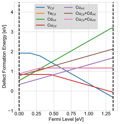
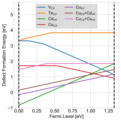
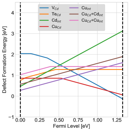
Copper (Cu) is well-known for enhancing carrier density in CdTe solar cells, leading to higher power conversion efficiency[47]. However, the doping instability of Cu and the presence of a large number of compensating defects[48, 49, 50] result in inferior efficiency and stability compared to group V-doped counterparts[47, 49]. To explore the dopability of Cu in CdTeSe, we calculated the formation energies of Cu defects under Cd-rich and Te-rich conditions (Fig. 10). Four dominant defects, , , and , along with the dominant intrinsic defects, are considered in this study.
Our calculations show that the defect transition level of (-1/0) in CdTe is 0.33 eV above the valence band maximum (VBM). Experimental results for this transition level vary between 0.15 and 0.37 eV[38, 51, 52, 53], with our result falling within the upper bound of this range, while HSE06 calculations suggest lower bound values around 0.20 eV[20]. Despite appearing deep in the gap, Cu can still act as an effective acceptor due to its relatively low formation energy, as shown in Fig. 10b. In CdTe, and emerge as dominant compensating defects, with the Fermi level being pinned around 0.3 eV, a significant improvement over intrinsic CdTe (Fig. 2b). However, as the Se ratio increases, the pinned level shifts toward the conduction band minimum (CBM) (Fig. 10d, Fig. 10f), rendering the system more -type. This shift suggests a decrease in the doping efficiency of Cu in CdTeSe, which may account for the observed degradation in net acceptor density in Cu-doped devices[49].
In conclusion, we believe that group V dopants hold more promise than Cu in CdTeSe alloys. Apart from the doping efficiency challenges associated with Cu in CdTeSe, Cu implantation in CdTe typically necessitates a Te-rich environment[54, 48], which may lead to the introduction of more deep-level traps, as illustrated in Fig. 2 and Fig. 10. In contrast, group V dopants generally favor a Cd-rich environment[55, 18], which can enhance carrier lifetime in solar cells.
IV Conclusions
In this study, we have undertaken a comprehensive investigation of intrinsic defects, copper, and group V dopants in CdTeSe alloys using density functional theory (DFT) calculations. Our tailored approach demonstrates its value, particularly during the convergence process as the supercell size increases. Systematic evaluations reveal that our refined methodology not only improves convergence characteristics but also delivers results that are more consistent with experimental data. Specifically, when analyzing defects such as AsTe and PTe, the transition levels calculated by our method show close agreement with experimental findings, underscoring the enhanced accuracy and reliability of our proposed approach.
Within the CdTeSe framework, the formation energy of point defects is noticeably influenced by the local spatial arrangement of Se and Te atoms. This phenomenon is notably evident in instances such as TeCd (+1, 0) and AsTe (+1), where the interplay of Se and Te positions exerts a pronounced effect. Our investigation extends beyond the mere identification of point defects to a deeper exploration of their intricate relationships with the local atomic environment.
Our study provides insights into the effects of arsenic and phosphorus defects on the electrical properties of CdTeSe alloy. We found that AX formation is more favorable in the alloy due to the interaction of selenium and group V species, which could potentially deteriorate the dopability of As/P in CdTeSe alloy. Our findings could help guide the development of new doping strategies for the fabrication of more efficient solar cells based on CdTeSe alloy.
Overall, we believe that group V dopants hold more promise than Cu in CdTeSe alloys, due to the doping efficiency challenges associated with Cu in CdTeSe and the potential introduction of more deep-level traps in a Te-rich environment. In contrast, group V dopants generally favor a Cd-rich environment, which can enhance carrier lifetime in solar cells.
In light of our findings, we conclude that optimizing the doping strategy and understanding the defect dynamics in CdTeSe are crucial for further improving the performance of optoelectronic devices based on this material. Future work will focus on integrating advanced simulation techniques, such as Lattice Monte Carlo simulations, continuum simulations and device simulation, to achieve a more detailed understanding of defect behavior in CdTeSe alloys and develop possible optimization strategy that could further enhance the efficiency and stability of CdTeSe-based optoelectronic devices.
Acknowledgements.
This work was supported by the U.S. Department of Energy’s Office of Energy Efficiency and Renewable Energy (EERE) under the Solar Energy Technology Office Award Number DE-EE0008556, NSF MRSEC DMR-1719797 and NSF MRSEC DMR-2308979. This work was facilitated through the use of the Hyak supercomputer system at the University of Washington provided via the Clean Energy Institute, the MEM-C MRSEC, and the Student Technology Fund. We also extend our gratitude to Dr. Darius Kuciauskas at the National Renewable Energy Laboratory (NREL) for fruitful discussions at the 50th IEEE Photovoltaic Specialists Conference (PVSC).Data Availability Statement
The data that support the findings of this study are available from the corresponding author upon reasonable request.
References
- Fiducia et al. [2019] T. A. Fiducia, B. G. Mendis, K. Li, C. R. Grovenor, A. H. Munshi, K. Barth, W. S. Sampath, L. D. Wright, A. Abbas, J. W. Bowers, et al., Nature Energy 4, 504 (2019).
- Wu et al. [2015] Y. Wu, G. Chen, Y. Zhu, W.-J. Yin, Y. Yan, M. Al-Jassim, and S. J. Pennycook, Computational Materials Science 98, 18 (2015).
- Xiang et al. [2023] X. Xiang, A. Gehrke, and S. Dunham, in 2023 IEEE 50th Photovoltaic Specialists Conference (PVSC) (IEEE, 2023) pp. 1–3.
- Castleton and Mirbt [2004] C. Castleton and S. Mirbt, Physical Review B 70, 195202 (2004).
- Schenk and Silber [1998] M. Schenk and C. Silber, Journal of Materials Science: Materials in Electronics 9, 295 (1998).
- Poplawsky et al. [2016] J. D. Poplawsky, W. Guo, N. Paudel, A. Ng, K. More, D. Leonard, and Y. Yan, Nature communications 7, 12537 (2016).
- Li et al. [2022] D.-B. Li, S. S. Bista, R. A. Awni, S. Neupane, A. Abudulimu, X. Wang, K. K. Subedi, M. K. Jamarkattel, A. B. Phillips, M. J. Heben, et al., Nature Communications 13, 7849 (2022).
- Kuciauskas et al. [2023] D. Kuciauskas, M. Nardone, A. Bothwell, D. Albin, C. Reich, C. Lee, and E. Colegrove, Advanced Energy Materials 13, 2301784 (2023).
- Okhotnikov et al. [2016] K. Okhotnikov, T. Charpentier, and S. Cadars, Journal of cheminformatics 8, 1 (2016).
- Landolt and Börnstein [1966] H. Landolt and R. Börnstein, Numerical data and functional relationships in science and technology: Crystal and solid state physics. Group 3, Vol. 7 (Springer-Verlag, 1966).
- Freysoldt et al. [2014] C. Freysoldt, B. Grabowski, T. Hickel, J. Neugebauer, G. Kresse, A. Janotti, and C. G. Van de Walle, Reviews of modern physics 86, 253 (2014).
- Freysoldt et al. [2009] C. Freysoldt, J. Neugebauer, and C. G. Van de Walle, Physical review letters 102, 016402 (2009).
- Komsa et al. [2012] H.-P. Komsa, T. T. Rantala, and A. Pasquarello, Physical Review B 86, 045112 (2012).
- [14] Y. Tong, X. Xiang, and S. T. Dunham, (unpublished) .
- Limas and Manz [2016] N. G. Limas and T. A. Manz, RSC advances 6, 45727 (2016).
- Manz and Limas [2016] T. A. Manz and N. G. Limas, RSC advances 6, 47771 (2016).
- Krasikov et al. [2016] D. Krasikov, A. Scherbinin, A. Knizhnik, A. Vasiliev, B. Potapkin, and T. Sommerer, Journal of Applied Physics 119 (2016).
- Nagaoka et al. [2020] A. Nagaoka, K. Nishioka, K. Yoshino, R. Katsube, Y. Nose, T. Masuda, and M. A. Scarpulla, Applied Physics Letters 116 (2020).
- Seeger [2013] K. Seeger, Semiconductor physics (Springer Science & Business Media, 2013).
- Yang et al. [2016] J.-H. Yang, W.-J. Yin, J.-S. Park, J. Ma, and S.-H. Wei, Semiconductor Science and Technology 31, 083002 (2016).
- Emanuelsson et al. [1993] P. Emanuelsson, P. Omling, B. Meyer, M. Wienecke, and M. Schenk, Physical Review B 47, 15578 (1993).
- Berding [1999] M. Berding, Physical Review B 60, 8943 (1999).
- Wei and Zhang [2002] S.-H. Wei and S. Zhang, Physical Review B 66, 155211 (2002).
- Chang et al. [2006] Y.-C. Chang, R. James, and J. Davenport, Physical Review B 73, 035211 (2006).
- Du et al. [2008] M.-H. Du, H. Takenaka, and D. J. Singh, Journal of Applied Physics 104 (2008).
- Castaldini et al. [1998] A. Castaldini, A. Cavallini, B. Fraboni, P. Fernandez, and J. Piqueras, Journal of applied physics 83, 2121 (1998).
- Reislöhner et al. [1998] U. Reislöhner, J. Grillenberger, and W. Witthuhn, Journal of crystal growth 184, 1160 (1998).
- Park et al. [2018] J. S. Park, S. Kim, Z. Xie, and A. Walsh, Nat. Rev. Mater. 3, 194 (2018).
- Stoneham [1981] A. Stoneham, Rep. Prog. Phys. 44, 1251 (1981).
- Alkauskas et al. [2014] A. Alkauskas, Q. Yan, and C. G. Van de Walle, Phys. Rev. B 90, 075202 (2014).
- Kim et al. [2019a] S. Kim, J.-S. Park, S. N. Hood, and A. Walsh, J. Mater. Chem. A 7, 2686 (2019a).
- Kim et al. [2019b] S. Kim, S. N. Hood, and A. Walsh, Phys. Rev. B 100, 041202 (2019b).
- Kavanagh et al. [2021] S. R. Kavanagh, A. Walsh, and D. O. Scanlon, ACS Energy Letters 6, 1392 (2021).
- Ma et al. [2013] J. Ma, D. Kuciauskas, D. Albin, R. Bhattacharya, M. Reese, T. Barnes, J. V. Li, T. Gessert, and S.-H. Wei, Physical review letters 111, 067402 (2013).
- Ma et al. [2014] J. Ma, J. Yang, S.-H. Wei, and J. L. Da Silva, Physical Review B 90, 155208 (2014).
- Mutter and Dunham [2015] D. Mutter and S. T. Dunham, IEEE Journal of Photovoltaics 5, 1188 (2015).
- Krasikov and Sankin [2017] D. Krasikov and I. Sankin, Journal of Materials Chemistry A 5, 3503 (2017).
- Balcioglu et al. [2000] A. Balcioglu, R. Ahrenkiel, and F. Hasoon, Journal of Applied Physics 88, 7175 (2000).
- Krasikov [2019] D. Krasikov, Nature Energy 4, 442 (2019).
- Xiang et al. [2021] X. Xiang, D. E. Sommer, A. Gehrke, and S. T. Dunham, in 2021 IEEE 48th Photovoltaic Specialists Conference (PVSC) (IEEE, 2021) pp. 1707–1711.
- Gehrke et al. [2023] A. S. Gehrke, D. E. Sommer, and S. T. Dunham, Journal of Applied Physics 134 (2023).
- Xiang et al. [2024] X. Xiang, D. E. Sommer, A. Gehrke, and S. T. Dunham, IEEE Journal of Photovoltaics (2024).
- Yang et al. [2015] J.-H. Yang, W.-J. Yin, J.-S. Park, J. Burst, W. K. Metzger, T. Gessert, T. Barnes, and S.-H. Wei, Journal of Applied Physics 118, 025102 (2015).
- Chatratin et al. [2023] I. Chatratin, B. Dou, S.-H. Wei, and A. Janotti, The Journal of Physical Chemistry Letters 14, 273 (2023).
- Krasikov and Sankin [2018] D. Krasikov and I. Sankin, Physical Review Materials 2, 103803 (2018).
- Dreyer et al. [2020] C. E. Dreyer, A. Alkauskas, J. L. Lyons, and C. G. Van de Walle, Physical Review B 102, 085305 (2020).
- Li et al. [2021] D.-B. Li, C. Yao, S. Vijayaraghavan, R. A. Awni, K. K. Subedi, R. J. Ellingson, L. Li, Y. Yan, and F. Yan, Nature Energy 6, 715 (2021).
- Artegiani et al. [2020] E. Artegiani, J. D. Major, H. Shiel, V. Dhanak, C. Ferrari, and A. Romeo, Solar Energy Materials and Solar Cells 204, 110228 (2020).
- Krasikov et al. [2021] D. Krasikov, D. Guo, S. Demtsu, and I. Sankin, Solar Energy Materials and Solar Cells 224, 111012 (2021).
- Chou et al. [1996] H. Chou, A. Rohatgi, N. Jokerst, E. Thomas, and S. Kamra, Journal of electronic materials 25, 1093 (1996).
- Gippius et al. [1974] A. Gippius, J. Panossian, and V. Chapnin, physica status solidi (a) 21, 753 (1974).
- Chamonal et al. [1982] J. Chamonal, E. Molva, and J. Pautrat, Solid State Communications 43, 801 (1982).
- Said and Kanehisa [1990] M. Said and M. Kanehisa, Journal of crystal growth 101, 488 (1990).
- Zhang et al. [2008] L. Zhang, J. L. Da Silva, J. Li, Y. Yan, T. Gessert, and S.-H. Wei, Physical review letters 101, 155501 (2008).
- Nagaoka et al. [2019] A. Nagaoka, K. Nishioka, K. Yoshino, D. Kuciauskas, and M. A. Scarpulla, Applied Physics Express 12, 081002 (2019).