SQUID oscillations in PbTe nanowire networks
Abstract
Network structures by semiconductor nanowires hold great promise for advanced quantum devices, especially for applications in topological quantum computing. In this study, we created networks of PbTe nanowires arranged in loop configurations. Using shadow-wall epitaxy, we defined superconducting quantum interference devices (SQUIDs) using the superconductor Pb. These SQUIDs exhibit oscillations in supercurrent upon the scanning of a magnetic field. Most of the oscillations can be fitted assuming a sinusoidal current-phase relation for each Josephson junction. Under certain conditions, the oscillations are found to be skewed, suggesting possible deviation from a sinusoidal behavior. Our results highlight the potential of PbTe nanowires for building complex quantum devices in the form of networks.
I Introduction
Semiconductor nanowires, as one-dimensional (1D) electron systems, are anticipated to harbor fascinating phases of matter, such as topological superconductivity when coupled to a superconductor [1, 2]. While the 1D device configuration greatly facilitates in electron tunability and confinement, it also renders challenges for more intricate device applications. Take Majorana zero modes for instance. While a single 1D wire can serve as a testbed to study relevant experimental signatures [3, 4, 5, 6, 7, 8], more complex device structures involving nanowire networks are essential for braiding experiments or topological qubits [9, 10, 11, 12, 13, 14]. The technique of selective-area-growth (SAG) offers a solution to this scalability issue, enabling the realization of complex network structures through lithography on demand.
Previous studies on SAG nanowire networks primarily focused on the Aharonov-Bohm effect, where conductance oscillations were observed in a magnetic field due to electron interference [15, 16, 17, 18]. Here, we present the interference of Cooper pairs (supercurrents) in nanowire networks coupled to a superconductor. We choose PbTe as the material, a promising candidate for Majorana nanowires that has recently emerged [19, 20, 21, 22, 23, 24, 25, 26, 27, 28, 29, 30, 31, 32]. Using shadow wall epitaxy of Pb superconducting film, we defined two Josephson junctions (JJs) within the network loop. The resulting dc superconducting quantum interference device (SQUID) exhibit a gate-tunable supercurrent. The supercurrent oscillates in a magnetic field based on which the underlying current-phase relation is discussed. Our results pave the way toward scalable nanowire network devices, with relevance to studies on Majorana zero modes [12, 13, 14, 33] and superconductor-semiconductor hybrid qubits [34, 35, 36, 37, 38, 39, 40].
II Device growth and fabrication
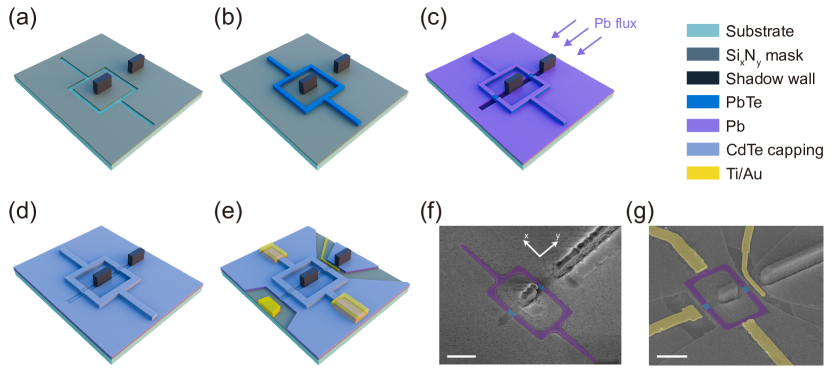
Figure 1 illustrates the key steps of the device growth and fabrication. Initially, a CdTe(001) substrate was covered with a thin film of Pb0.92Eu0.08Te and a CdTe capping layer, grown in a molecular beam epitaxy chamber. Next, a SiN dielectric was deposited on the substrate, and network trenches were defined using reactive ion etching (Fig. 1(a)). Two shadow walls were constructed before these processing steps. Subsequently, PbTe nanowires were selectively grown within the network structure (Fig. 1(b)), followed by the low-temperature deposition of Pb using shadow-wall epitaxy (Fig. 1(c)). The chip was then capped by a thin layer of CdTe (Fig. 1(d)).
Each shadow wall defines a JJ in each “arm” of the loop. The two JJs thus form a dc SQUID via the PbTe network. Figure 1(f) is a tilted scanning electron micrograph (SEM) of a representative SQUID. Further details on this growth procedure can be found in Ref. [30].
After growth, contacts and side gates were fabricated as shown in Figs. 1(e) and 1(g). To prevent short-circuiting, the regions of Pb film beneath the gates were etched away prior to the gate deposition. Argon plasma etching was conducted in situ before contact deposition to remove the CdTe capping, ensuring ohmic contacts. Devices based on individual PbTe-Pb nanowires grown using the same protocol have exhibited an atomically sharp PbTe-Pb interface, a hard superconducting gap, and gate-tunable supercurrents [24, 26]. These findings indicate the high quality of the hybrid nanowires, sufficient for the realization of more intricate network devices.
III SQUID oscillations in device A
Four dc SQUIDs (devices A-D) with varying loop areas were measured, all exhibiting similar behavior. Figure 2(a) presents the SEM of device A (without tilting). The gate voltages applied to the bottom and top gates are denoted as and , respectively. The measurements were conducted using a standard two-terminal set-up in a dilution refrigerator with a base temperature below 50 mK. Any series resistance, arising from the fridge filters and device contacts, has been subtracted during data processing similar to that in Ref. [24].
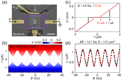
Figure 2(b) shows the voltage drop () across the SQUID as a function of current () and magnetic field () for device A. was perpendicular to the device substrate throughout the measurement (unless specified). and were kept grounded. The white region represents the zero-resistance supercurrent regime. Periodic oscillations of the supercurrent are observed with a period 13.7 Gs. Using the formula , we can convert this period to an effective area () 1.50 m2, where denotes the flux quantum, is the Plank constant and is the electron charge. The spacing between the top and bottom JJs is 1.5 m. The effective area corresponds to an effective width of 1 m, as indicated by the white dashed box in Fig. 1(a). The box size is larger than the shadowed region but smaller than the network loop, possibly due to the penetration effect of and flux focusing. Figure 2(c) presents two line cuts with the minimal and maximum switching currents, i.e. 0.3 A and 1.1 A, respectively. Assuming the critical currents of the two JJs are and , we then extract = 0.7 A, = 0.4 A, based on = 1.1 A and = 0.3 A. It is assumed that the switching current is close to the critical current, as the fridge temperature is much less than the Josephson energy.
In Fig. 2(d), we plot the switching current, , extracted from Fig. 2(b). The red curve represents a fit with no fitting parameters (except for a phase offset), assuming a sinusoidal current-phase relation: sin, sin . and are the currents passing through the two JJs, and and are the phase drops over the two JJs. The phases and the magnetic flux through the effective area are related by . We have assumed that the contribution from the loop inductance, , is negligible, as the positions of maximum switching current for positive and negative biases are nearly identical. Here, denotes the SQUID inductance and represents the circulating current in the loop. The switching current can then be calculated as . We plot this formula, based on the extracted and , as the red curve in Fig. 2(d), which agrees reasonably well with the experimental data.
IV Gate dependence of SQUID oscillations in device A
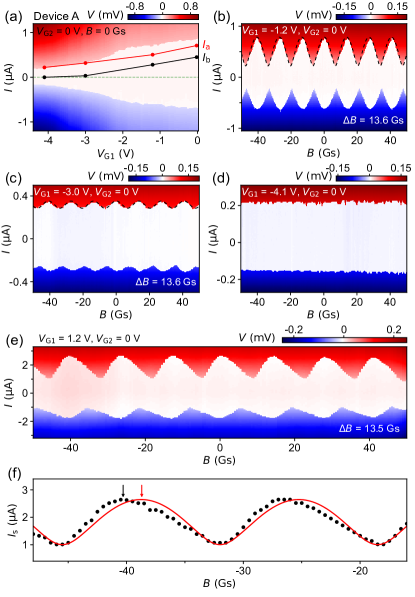
Next, we investigate the gate dependence of device A. Figure 3(a) shows the supercurrent as a function of at = 0 T, revealing a monotonically decreasing trend in . To determine the critical current of each JJ, we conduct the SQUID measurements at four settings, as illustrated in Fig. 2(b) and Figs. 3(b-d). From the maximum and minimum switching currents of the SQUID oscillations, we infer and , and mark them in Fig. 3(a) as red and black dots, respectively. Despite the significant distance between the G1 gate and the top JJ (nearly 2 m), can still simultaneously modulate the critical currents of both JJs with similar amplitudes. This strong capacitive coupling arises from the global distribution of the PbEuTe substrate, as detailed in Ref. [30] (Fig. S5).
The dashed lines in Figs. 3(b-c) depict fits using the aforementioned method. The fit roughly matches the oscillations with minor deviations, indicating a sinusoidal current-phase relation for both JJs over a considerable gate range. As decreases, the amplitudes of SQUID oscillations diminish while the periods () remain unchanged. In Fig. 3(d), no oscillations are observed, suggesting that the supercurrent in one JJ has been turned off.
Following this, a skewed oscillation pattern is observed at = 1.2 V, as illustrated in Fig. 3(e). Figure 3(f) presents the extracted switching currents (depicted as black dots) alongside the fit (represented by the red curve), assuming a sinusoidal current-phase relation of the JJs. For the sake of clarity only two periods are plotted. Notably, the position of maximum (indicated by the black arrow) does not align with the center of the two ’s corresponding to the minimum (denoted by the red arrow), indicative of the observed the skewness. Such deviation, also (barely) visible in Fig. 2(b), may imply deviations from a sinusoidal current-phase relation. A non-sinusoidal case is commonly expected for S-N-S JJs exhibiting high junction transparency [41, 42] (S represents superconductor and N denotes normal conductor). While a sinusoidal current-phase relation is typically a valid approximation in scenarios when the junction transmission is small, it may not hold for high transparent junctions. It is essential to note that the current-phase relation cannot be directly discerned from in Fig. 3(f), especially considering that the two JJs are not in the high asymmetry regime. Even in instances of high asymmetry, i.e. , the conventional approach of using as an approximation of [43, 44, 45] has its inherent limitations [46, 47]. For an overview of SQUID oscillations in device A at various settings, we refer to Fig. S1 in the Supplementary Material.
V SQUID oscillations in additional devices
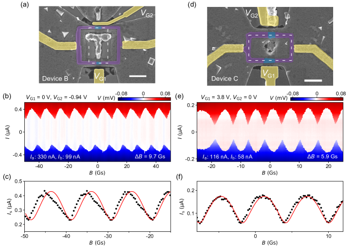
Figure 4 presents two additional devices with varying network sizes (loop areas), showcasing analogous behavior. In Fig. 4(a), the SEM of device B reveals triangle debris outside loop, attributed to PbTe parasitic growth, as the selectivity of this particular growth is slightly inferior. The shadow wall adopted a T shape, resulting in a larger shadowed region inside the loop compared to device A. The loop size is also larger. Consequently, the period of the SQUID oscillations in Fig. 4(b), denoted as 9.7 Gs, is smaller than that observed in device A. This period can be converted to an effective area of 2.12 m2, as indicated by the white dashed box in Fig. 4(a). The extracted switching current (depicted as black dots in Fig. 4(c)) exhibits deviation from the fit (illustrated by the red curve), similar to the behavior observed in Fig. 3(f). The skewed portion has a shoulder/kink structure near of 0.35 A, reminiscent of the current-phase relation of Andreev bound states in the presence of charging energy [48].
Figure 4(d) shows the SEM of a third device. The shadow wall inside the loop detached from the substrate chip during the device fabrication process. The effective area, determined based on the period of the SQUID oscillations in Fig. 4(e), is 3.5 m2, as indicated by the white dashed box. Unlike devices A and B, the box size matches the network loop of device C. The underlying mechanisms governing flux focusing and penetration for each specific device remain unclear. Nevertheless, the oscillations in device C are roughly consistent with a sinusoidal current-phase relation, as shown in Fig. 4(f). For additional SQUID oscillations of devices B and C at various gate settings, we refer to Figs. S2 and S3 in the Supplementary Material. Furthermore, Fig. S4 depicts a fourth device, which also exhibits gate-tunable SQUID oscillations.
VI Conclusion and Outlook
In summary, we have realized dc SQUIDs using selective-area-grown PbTe-Pb nanowire networks. These networks exhibit tunable supercurrents and SQUID oscillations in response to a magnetic field. The underlying current-phase relations have been explored. The PbTe-Pb hybrid nanowires hold promise for advancing topological quantum computation in the quest for Majorana zero modes. While transport studies on individual nanowires offer valuable insights, they are insufficient for definitive proving the existence of Majoranas. Braiding experiments, necessitating intricate network architectures, are imperative for conclusive validation. Our results represent a stride toward scalable network devices, heralding prospects for more intricate geometries such as topological qubits.
Raw data and processing codes within this paper are available at https://doi.org/10.5281/zenodo.10952569
VII Acknowledgment
This work is supported by National Natural Science Foundation of China (92065206) and the Innovation Program for Quantum Science and Technology (2021ZD0302400).
References
- Lutchyn et al. [2010] R. M. Lutchyn, J. D. Sau, and S. Das Sarma, Majorana fermions and a topological phase transition in semiconductor-superconductor heterostructures, Phys. Rev. Lett. 105, 077001 (2010).
- Oreg et al. [2010] Y. Oreg, G. Refael, and F. von Oppen, Helical liquids and Majorana bound states in quantum wires, Phys. Rev. Lett. 105, 177002 (2010).
- Mourik et al. [2012] V. Mourik, K. Zuo, S. M. Frolov, S. Plissard, E. P. Bakkers, and L. P. Kouwenhoven, Signatures of Majorana fermions in hybrid superconductor-semiconductor nanowire devices, Science 336, 1003 (2012).
- Deng et al. [2016] M. Deng, S. Vaitiekėnas, E. B. Hansen, J. Danon, M. Leijnse, K. Flensberg, J. Nygård, P. Krogstrup, and C. M. Marcus, Majorana bound state in a coupled quantum-dot hybrid-nanowire system, Science 354, 1557 (2016).
- Albrecht et al. [2016] S. Albrecht, A. Higginbotham, M. Madsen, F. Kuemmeth, T. Jespersen, J. Nygård, P. Krogstrup, and C. Marcus, Exponential protection of zero modes in Majorana islands, Nature 531, 206 (2016).
- Gül et al. [2018] Ö. Gül, H. Zhang, J. D. Bommer, M. W. de Moor, D. Car, S. R. Plissard, E. P. Bakkers, A. Geresdi, K. Watanabe, T. Taniguchi, et al., Ballistic Majorana nanowire devices, Nature Nanotechnology 13, 192 (2018).
- Song et al. [2022] H. Song, Z. Zhang, D. Pan, D. Liu, Z. Wang, Z. Cao, L. Liu, L. Wen, D. Liao, R. Zhuo, et al., Large zero bias peaks and dips in a four-terminal thin InAs-Al nanowire device, Phys. Rev. Research 4, 033235 (2022).
- Wang et al. [2022] Z. Wang, H. Song, D. Pan, Z. Zhang, W. Miao, R. Li, Z. Cao, G. Zhang, L. Liu, L. Wen, et al., Plateau regions for zero-bias peaks within 5 of the quantized conductance value , Phys. Rev. Lett. 129, 167702 (2022).
- Alicea et al. [2010] J. Alicea, Y. Oreg, G. Refael, F. von Oppen, and M. P. A. Fisher, Non-Abelian statistics and topological quantum information processing in 1D wire networks, Nature Physics 7, 412 (2010).
- Hyart et al. [2013] T. Hyart, B. van Heck, I. C. Fulga, M. Burrello, A. R. Akhmerov, and C. W. J. Beenakker, Flux-controlled quantum computation with Majorana fermions, Phys. Rev. B 88, 035121 (2013).
- Aasen et al. [2016] D. Aasen, M. Hell, R. V. Mishmash, A. Higginbotham, J. Danon, M. Leijnse, T. S. Jespersen, J. A. Folk, C. M. Marcus, K. Flensberg, and J. Alicea, Milestones toward Majorana-based quantum computing, Phys. Rev. X 6, 031016 (2016).
- Vijay and Fu [2016] S. Vijay and L. Fu, Teleportation-based quantum information processing with Majorana zero modes, Phys. Rev. B 94, 235446 (2016).
- Plugge et al. [2017] S. Plugge, A. Rasmussen, R. Egger, and K. Flensberg, Majorana box qubits, New Journal of Physics 19, 012001 (2017).
- Karzig et al. [2017] T. Karzig, C. Knapp, R. M. Lutchyn, P. Bonderson, M. B. Hastings, C. Nayak, J. Alicea, K. Flensberg, S. Plugge, Y. Oreg, C. M. Marcus, and M. H. Freedman, Scalable designs for quasiparticle-poisoning-protected topological quantum computation with Majorana zero modes, Phys. Rev. B 95, 235305 (2017).
- Vaitiekėnas et al. [2018] S. Vaitiekėnas, A. M. Whiticar, M.-T. Deng, F. Krizek, J. E. Sestoft, C. J. Palmstrøm, S. Marti-Sanchez, J. Arbiol, P. Krogstrup, L. Casparis, and C. M. Marcus, Selective-area-grown semiconductor-superconductor hybrids: A basis for topological networks, Phys. Rev. Lett. 121, 147701 (2018).
- Lee et al. [2019] J. S. Lee, S. Choi, M. Pendharkar, D. J. Pennachio, B. Markman, M. Seas, S. Koelling, M. A. Verheijen, L. Casparis, K. D. Petersson, et al., Selective-area chemical beam epitaxy of in-plane InAs one-dimensional channels grown on InP(001), InP(111)b, and InP(011) surfaces, Phys. Rev. Mater. 3, 084606 (2019).
- Aseev et al. [2019] P. Aseev, G. Wang, L. Binci, A. Singh, S. Martí-Sánchez, M. Botifoll, L. Stek, A. Bordin, J. Watson, F. Boekhout, et al., Ballistic InSb nanowires and networks via metal-sown selective area growth, Nano Letters 19, 9102 (2019).
- het Veld et al. [2020] R. L. M. O. het Veld, D. Xu, V. Schaller, M. A. Verheijen, S. M. E. Peters, J. Jung, C. Tong, Q. Wang, M. W. A. de Moor, B. Hesselmann, et al., In-plane selective area InSb–Al nanowire quantum networks, Communications Physics 3, 59 (2020).
- Cao et al. [2022] Z. Cao, D. E. Liu, W.-X. He, X. Liu, K. He, and H. Zhang, Numerical study of PbTe-Pb hybrid nanowires for engineering Majorana zero modes, Phys. Rev. B 105, 085424 (2022).
- Jiang et al. [2022] Y. Jiang, S. Yang, L. Li, W. Song, W. Miao, B. Tong, Z. Geng, Y. Gao, R. Li, F. Chen, Q. Zhang, F. Meng, L. Gu, K. Zhu, Y. Zang, R. Shang, Z. Cao, X. Feng, Q.-K. Xue, D. E. Liu, H. Zhang, and K. He, Selective area epitaxy of PbTe-Pb hybrid nanowires on a lattice-matched substrate, Phys. Rev. Materials 6, 034205 (2022).
- Jung et al. [2022] J. Jung, S. G. Schellingerhout, M. F. Ritter, S. C. ten Kate, O. A. van der Molen, S. de Loijer, M. A. Verheijen, H. Riel, F. Nichele, and E. P. Bakkers, Selective area growth of PbTe nanowire networks on InP, Advanced Functional Materials 32, 2208974 (2022).
- Geng et al. [2022] Z. Geng, Z. Zhang, F. Chen, S. Yang, Y. Jiang, Y. Gao, B. Tong, W. Song, W. Miao, R. Li, Y. Wang, Q. Zhang, F. Meng, L. Gu, K. Zhu, Y. Zang, L. Li, R. Shang, X. Feng, Q.-K. Xue, K. He, and H. Zhang, Observation of Aharonov-Bohm effect in PbTe nanowire networks, Phys. Rev. B 105, L241112 (2022).
- ten Kate et al. [2022] S. C. ten Kate, M. F. Ritter, A. Fuhrer, J. Jung, S. G. Schellingerhout, E. P. A. M. Bakkers, H. Riel, and F. Nichele, Small charging energies and g-factor anisotropy in PbTe quantum dots, Nano Letters 22, 7049 (2022).
- Zhang et al. [2023] Z. Zhang, W. Song, Y. Gao, Y. Wang, Z. Yu, S. Yang, Y. Jiang, W. Miao, R. Li, F. Chen, Z. Geng, Q. Zhang, F. Meng, T. Lin, L. Gu, K. Zhu, Y. Zang, L. Li, R. Shang, X. Feng, Q.-K. Xue, K. He, and H. Zhang, Proximity effect in PbTe-Pb hybrid nanowire Josephson junctions, Phys. Rev. Mater. 7, 086201 (2023).
- Song et al. [2023] W. Song, Y. Wang, W. Miao, Z. Yu, Y. Gao, R. Li, S. Yang, F. Chen, Z. Geng, Z. Zhang, S. Zhang, Y. Zang, Z. Cao, D. E. Liu, R. Shang, X. Feng, L. Li, Q.-K. Xue, K. He, and H. Zhang, Conductance quantization in PbTe nanowires, Phys. Rev. B 108, 045426 (2023).
- Gao et al. [2024] Y. Gao, W. Song, S. Yang, Z. Yu, R. Li, W. Miao, Y. Wang, F. Chen, Z. Geng, L. Yang, Z. Xia, X. Feng, Y. Zang, L. Li, R. Shang, Q.-K. Xue, K. He, and H. Zhang, Hard superconducting gap in PbTe nanowires, Chinese Physics Letters 41, 038502 (2024).
- Wang et al. [2023] Y. Wang, F. Chen, W. Song, Z. Geng, Z. Yu, L. Yang, Y. Gao, R. Li, S. Yang, W. Miao, W. Xu, Z. Wang, Z. Xia, H.-D. Song, X. Feng, T. Wang, Y. Zang, L. Li, R. Shang, Q. Xue, K. He, and H. Zhang, Ballistic PbTe nanowire devices, Nano Letters 23, 11137 (2023).
- Li et al. [0] R. Li, W. Song, W. Miao, Z. Yu, Z. Wang, S. Yang, Y. Gao, Y. Wang, F. Chen, Z. Geng, L. Yang, J. Xu, X. Feng, T. Wang, Y. Zang, L. Li, R. Shang, Q. Xue, K. He, and H. Zhang, Selective-area-grown PbTe-Pb planar Josephson junctions for quantum devices, Nano Letters 0, null (0).
- Gupta et al. [2023] M. Gupta, V. Khade, C. Riggert, L. Shani, G. Menning, P. Lueb, J. Jung, R. Melin, E. P. A. M. Bakkers, and V. S. Pribiag, Evidence for -shifted Cooper quartets in PbTe nanowire three-terminal Josephson junctions, arXiv: 2312.17703 (2023).
- Song et al. [2024] W. Song et al., Reducing disorder in PbTe nanowires for Majorana research, arXiv: 2402.02132 (2024).
- Geng et al. [2024] Z. Geng et al., Epitaxial Indium on PbTe nanowires for quantum devices, arXiv: 2402.04024 (2024).
- Wang et al. [2024] Y. Wang et al., Gate-tunable subband degeneracy in semiconductor nanowires, (2024), arXiv:2404.02760 .
- Zhang et al. [2019] H. Zhang, D. E. Liu, M. Wimmer, and L. P. Kouwenhoven, Next steps of quantum transport in Majorana nanowire devices, Nature Communications 10, 5128 (2019).
- Larsen et al. [2015] T. W. Larsen, K. D. Petersson, F. Kuemmeth, T. S. Jespersen, P. Krogstrup, J. Nygård, and C. M. Marcus, Semiconductor-nanowire-based superconducting qubit, Phys. Rev. Lett. 115, 127001 (2015).
- de Lange et al. [2015] G. de Lange, B. van Heck, A. Bruno, D. J. van Woerkom, A. Geresdi, S. R. Plissard, E. P. A. M. Bakkers, A. R. Akhmerov, and L. DiCarlo, Realization of microwave quantum circuits using hybrid superconducting-semiconducting nanowire Josephson elements, Phys. Rev. Lett. 115, 127002 (2015).
- Hays et al. [2021] M. Hays, V. Fatemi, D. Bouman, J. Cerrillo, S. Diamond, K. Serniak, T. Connolly, P. Krogstrup, J. Nygård, A. L. Yeyati, A. Geresdi, and M. H. Devoret, Coherent manipulation of an Andreev spin qubit, Science 373, 430 (2021).
- Huo et al. [2023] J. Huo, Z. Xia, Z. Li, S. Zhang, Y. Wang, D. Pan, Q. Liu, Y. Liu, Z. Wang, Y. Gao, J. Zhao, T. Li, J. Ying, R. Shang, and H. Zhang, Gatemon qubit based on a thin InAs-Al hybrid nanowire, Chinese Physics Letters 40, 047302 (2023).
- Pita-Vidal et al. [2023] M. Pita-Vidal, A. Bargerbos, R. Žitko, L. Splitthoff, L. Grünhaupt, J. Wesdorp, Y. Liu, L. Kouwenhoven, R. Aguado, B. Heck, A. Kou, and C. Andersen, Direct manipulation of a superconducting spin qubit strongly coupled to a transmon qubit, Nature Physics 19, 1110 (2023).
- Xia et al. [2024] Z. Xia, J. Huo, Z. Li, J. Ying, Y. Liu, X.-Y. Tang, Y. Wang, M. Chen, D. Pan, S. Zhang, Q. Liu, T. Li, L. Li, K. He, J. Zhao, R. Shang, and H. Zhang, Gate-compatible circuit quantum electrodynamics in a three-dimensional cavity architecture, Phys. Rev. Appl. 21, 034031 (2024).
- Aguado [2020] R. Aguado, A perspective on semiconductor-based superconducting qubits, Applied Physics Letters 117, 240501 (2020).
- Beenakker [1991] C. W. J. Beenakker, Universal limit of critical-current fluctuations in mesoscopic Josephson junctions, Phys. Rev. Lett. 67, 3836 (1991).
- Spanton et al. [2017] E. M. Spanton, M. Deng, S. Vaitiekėnas, P. Krogstrup, J. Nygård, C. M. Marcus, and K. A. Moler, Current–phase relations of few-mode InAs nanowire Josephson junctions, Nature Physics 13, 1177 (2017).
- Della Rocca et al. [2007] M. L. Della Rocca, M. Chauvin, B. Huard, H. Pothier, D. Esteve, and C. Urbina, Measurement of the current-phase relation of superconducting atomic contacts, Phys. Rev. Lett. 99, 127005 (2007).
- Nanda et al. [2017] G. Nanda, J. L. Aguilera-Servin, P. Rakyta, A. Kormányos, R. Kleiner, D. Koelle, K. Watanabe, T. Taniguchi, L. M. K. Vandersypen, and S. Goswami, Current-phase relation of ballistic graphene Josephson junctions, Nano Letters 17, 3396 (2017).
- Murani et al. [2016] A. Murani, A. Y. Kasumov, S. Sengupta, Y. A. Kasumov, V. T. Volkov, I. I. Khodos, F. Brisset, R. Delagrange, A. D. Chepelianskii, R. Deblock, H. ’el ene Bouchiat, and S. Guéron, Ballistic edge states in bismuth nanowires revealed by SQUID interferometry, Nature Communications 8 (2016).
- Endres et al. [2023] M. Endres, A. Kononov, H. S. Arachchige, J. Yan, D. Mandrus, K. Watanabe, T. Taniguchi, and C. Schönenberger, Current–phase relation of a WTe2 Josephson junction, Nano Letters 23, 4654 (2023).
- Babich et al. [2023] I. Babich, A. Kudriashov, D. Baranov, and V. S. Stolyarov, Limitations of the current–phase relation measurements by an asymmetric dc-SQUID, Nano Letters 23, 6713 (2023).
- Hart et al. [2019] S. Hart, Z. Cui, G. Ménard, M. Deng, A. E. Antipov, R. M. Lutchyn, P. Krogstrup, C. M. Marcus, and K. A. Moler, Current-phase relations of InAs nanowire Josephson junctions: From interacting to multimode regimes, Phys. Rev. B 100, 064523 (2019).
See pages 1 of PbTe_SQUID_SM.pdf See pages 2 of PbTe_SQUID_SM.pdf See pages 3 of PbTe_SQUID_SM.pdf See pages 4 of PbTe_SQUID_SM.pdf