Reconfigurable Multiple-Valued Logic Function and Sequential Circuit Realizations via Threshold Logic Gates
Abstract
In this paper, we present a general reconfigurable multiple-valued logic circuit. The proposed architecture is based on threshold logic gate and is compatible with binary logic, which allows a designer to easily integrate multiple valued logic with binary logic. We also present a methodology to design sequential circuits.
keywords:
Multiple-valued logic, Threshold logic gate, Nary decoder, Nary multiplexer, Nary sequential circuits, Nary reconfigurable computing.1 Introduction
Reconfigurable devices have been extensively used while realizing binary logic circuits. The first reconfigurable logic devices were based on the programmable array logic (PAL) architecture containing an array of AND and OR gates. PAL architectures are capable of executing any Boolean logic expression as a two-level sum-of-products function. However, they require quadratically more number of programmable switches as their logic capacity increases. This limits their scalability. Complex programmable logic devices (CPLDs) aimed to address the scalability issue by integrating multiple PALs on the same die, interconnected through a crossbar. Scalability of reconfigurable devices significantly improved after the introduction of look up table (LUT) based FPGA by Xilinx in 1984. LUT based architectures have much higher area efficiency compared to PALs and CPLDs. Later, and-inverter cone approach was proposed in [10] and field programable transistor array was presented in [12]. LUT based architectures are the dominant architectures in today’s commercial FPGAs. The interested reader should check [2] for a more detailed review on the evolution of binary FPGA architectures.
A recent survey on the existing designs and techniques for FPGA logic cells is presented in [11]. The paper also examines how emerging technologies and innovative micro-architectures strive to improve performance. The design in [8] leverages the ambipolar property of double-gate CNTFETs to reduce the delay of reconfigurable cells. An ambipolar device may be configured as either n-type or p-type. An FPGA implementation based on dynamic logic cell architecture is presented in [6], where the logic cells utilize silicon nano-wire ambipolar devices. A spintronic based FPGA implementation alternative to LUT-based CMOS reconfigurable logic is presented in [15]. In [7], Configurable memristive logic block (CMLB) are build via connecting memristive logic cells using memristive switch matrix cells. The CMLB is then used to construct a memristor-based FPGA architecture.
Traditional binary logic confines each wire to just two distinct voltage levels (representing 0 and 1) in a reconfigurable device. This approach has limitations in representing the inherent real world complexities and uncertainties while enabling efficient computation. Multi-valued logic offers an alternative by expanding beyond binary encoding. Multi-valued logic circuits leverage N distinct voltage levels to represent N different values. This effectively compresses information into a smaller spatial footprint, consequently demanding fewer routing resources and ultimately resulting in a reduction in chip area. This reduction translates directly to cost savings for the circuit designer. In this study, we will interchangeably call multi-valued logic as Nary logic as an extension of binary logic.
Several technologies offer devices that could potentially be used for multi-valued logic applications. A review of such devices, focusing on their operating principles, technologies, and applications, is presented in [1]. Although having high potential in implementation, only a few studies examine how multi-valued logic can be applied in a reconfigurable device. A quaternary look up table (LUT) architecture entirely implemented in CMOS technology is presented in [5]. This design necessitated the use of multiple supply voltages and transistors with distinct threshold voltages. The study in [9] introduces a quaternary configurable logic block (CLB) which incorporates dedicated quaternary carry propagation logic and quaternary flip-flops. In [3] an alternative quaternary LUT architecture, compatible with standard CMOS technology, is introduced. This design employs a single-level multiplexer to achieve reduced output resistance. The study in [4] implemented a quaternary FPGA architecture on an FDSOI technology.
Prior works, such as [14], employed threshold logic gates (TLG) within binary FPGA architectures. To our knowledge, no studies to date investigated the utilization of TLG for reconfigurable multi-valued logic circuits. Therefore, we propose a framework for implementing multi-valued reconfigurable logic functions in this study. This framework allows the utilization of Nary logic for both input and output signals, while maintaining compatibility with binary logic operations. This approach targets a reduction in wire congestion, potentially leading to lower chip cost. The proposed framework is build upon TLG based Nary decoder and multiplexer circuits. These building blocks are then used to implement multi-valued logic functions and sequential circuits in a reconfigurable manner.
Layout of the study is as follows. Abstract form of the TLG is introduced in Section 2. Nary decoder and multiplexer circuits based on TLG are introduced in Sections 3 and 4, respectively. These building blocks are then used to implement multi-valued logic functions in Section 5. Section 6 generalizes the idea to reconfigurable circuits. Section 7 focuses on reconfigurable sequential circuit implementations. Finally, Section 8 provides concluding remarks and future directions.
2 Threshold Logic Gate
The framework for implementing Nary reconfigurable logic functions in this study depends on TLG. Therefore, we first introduce it in this section. The TLG used in this study has two inputs as and . It compares its inputs and outputs a binary logic level 1 if , binary logic level 0 otherwise. We will use the symbol in Fig. 1 for the TLG circuit.
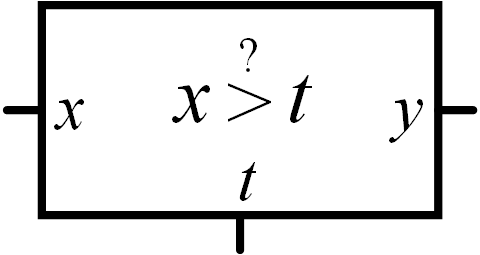
For the implementation details of this Transistor-Level Gate (TLG), we refer the reader to our previous work [13]. This specific implementation offers a built-in latch, simplifying the design of sequential circuits. However, the framework presented in this paper can also be implemented with other TLG architectures. Throughout the paper, we will employ an abstract representation of the circuits. Therefore, we will focus on the presented framework rather than the underlying transistor-level details.
3 Nary Decoder Formation via TLG
We will benefit from Nary decoders as our first option to implement multiple-valued logic functions. Therefore, we will start with defining the Nary decoder in this section. This decoder works such that only one of its outputs is set to binary logic level 1 and rest of outputs are kept at logic level 0 depending on the Nary input. We will form Nary decoders via TLG by first proposing a one-to- decoder. Then, we will extend the approach to -to- decoder formation, where is the number of Nary inputs to the decoder.
3.1 One-to- Decoder Formation
A one-to- decoder has one Nary input with possible values. Output of the decoder is pins, each being binary logic level 0 or 1 based on the given input. The Nary decoder will have one-hot output as in binary decoders. Hence, only one output pin will be at logic level 1 for the given Nary input.
We can represent the proposed one-to- decoder mathematically as follows. Let be the Nary input to the decoder. outputs of the decoder will be for . For the given Nary input , only output will be logic level 1. The remaining values will be logic level 0. Hence, one-hot output representation is satisfied.
We can realize the one-to- decoder via TLGs and binary logic gates. We provide the proposed structure in Fig. 2. As can be seen in this figure, operation of the circuit resembles a flash type analog-to-digital converter such that Nary input is compared against threshold values.
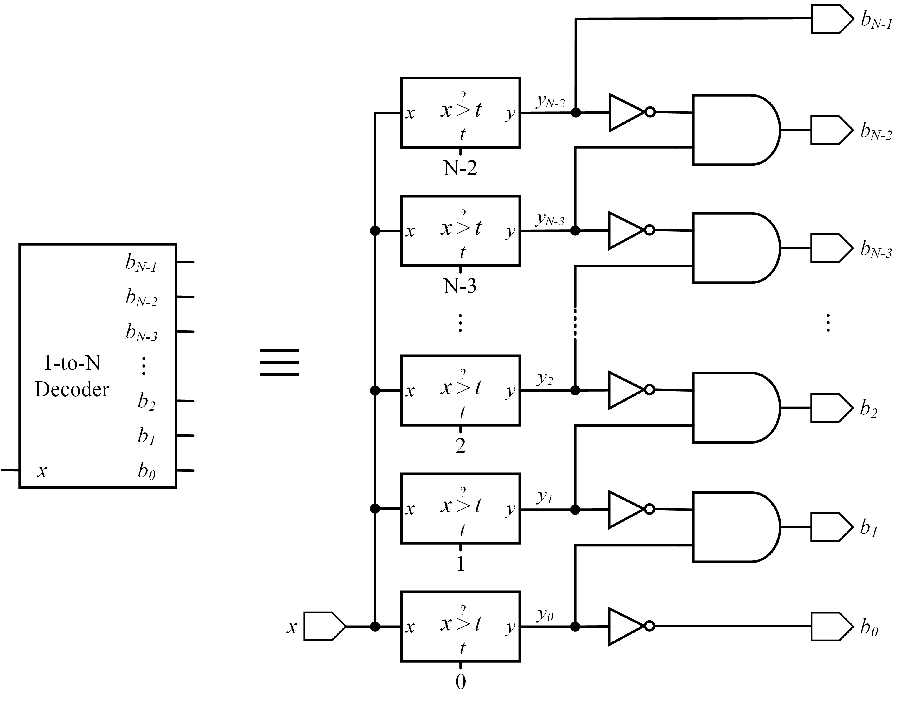
As can be seen in Fig. 2, output of TLGs for the input will be for . Binary AND gates in the figure convert outputs to one-hot output representation as for . Here, represents the binary AND gate. indicates the binary NOT of . Outputs and do not exist in the implementation given in Fig. 2. They are included in the representation for mathematical completeness. Therefore, they should be taken as 1 and 0 in implementation, respectively.
Let’s consider the ternary decoder with to clarify our discussion. Hence, the circuit in Fig. 2 simplifies such that there are two TLGs with threshold values as 1 and 0, respectively. We provide the truth table formed for the ternary decoder in Table 1. Here, is the ternary input; , , and are decoder outputs. As can be seen in the table, only one output has logic level 1 for a given ternary input.
| Input | Output | ||
|---|---|---|---|
| 0 | 0 | 0 | 1 |
| 1 | 0 | 1 | 0 |
| 2 | 1 | 0 | 0 |
3.2 -to- Decoder Formation
We can form the -to- decoder following the procedure in the previous section. To do so, we should first decompose it to one-to- decoders. Then, we can merge outputs of one-to- decoders via binary AND gates to reach the final -to- decoder. Let’s explain the procedure on a simple example.
Assume that we would like to form a two-to- decoder with two Nary inputs , . This decoder can be constructed by using two one-to- decoders. The first decoder decodes the input and generates outputs for . The second decoder decodes the input and generates outputs for . We will have and to be at logic level 1 for the Nary input . All the remaining outputs will be logic level 0. Therefore, outputs of the two-to- decoder can be formed by logically ANDing output of the first and second decoders and , respectively. Thus, only one output of the two-to- decoder will be at logic level 1. All other outputs will be at logic level 0 for a given input.
We can generalize our methodology to the -to- decoder by representing its input as . Outputs of the decoder for can be obtained by ANDing corresponding outputs of one-to- decoders. Therefore, th output of the -to- decoder will be
| (1) |
where and is the th output of the th 1-to- decoder. The value is calculated as where the floor function calculates the greatest integer less than or equal to its argument. The product operation is used to represent AND operations in Eqn. 1. Output of the decoder is one-hot such that only one is set to logic level 1. The remaining outputs are set to logic level 0.
We provide truth table of the two-to-nine decoder in Table 2 as an example. As can be seen in this table, we formed this decoder by using two one-to-three decoders and binary AND operations represented by the sign.
| 0 | 0 | 0 | 0 | 1 | 0 | 0 | 1 | |
| 0 | 1 | 0 | 0 | 1 | 0 | 1 | 0 | |
| 0 | 2 | 0 | 0 | 1 | 1 | 0 | 0 | |
| 1 | 0 | 0 | 1 | 0 | 0 | 0 | 1 | |
| 1 | 1 | 0 | 1 | 0 | 0 | 1 | 0 | |
| 1 | 2 | 0 | 1 | 0 | 1 | 0 | 0 | |
| 2 | 0 | 1 | 0 | 0 | 0 | 0 | 1 | |
| 1 | 1 | 1 | 0 | 0 | 0 | 1 | 0 | |
| 2 | 2 | 1 | 0 | 0 | 1 | 0 | 0 |
4 Nary Multiplexer Formation via Nary Decoder
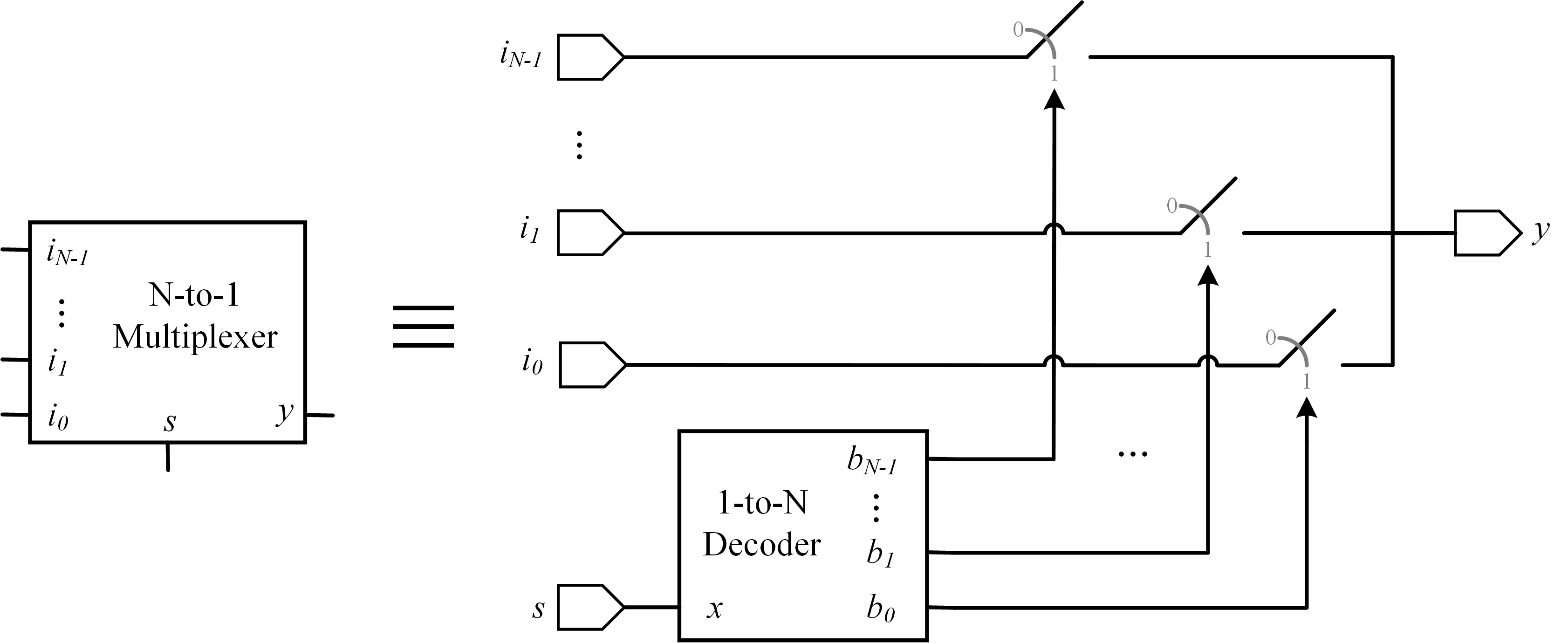
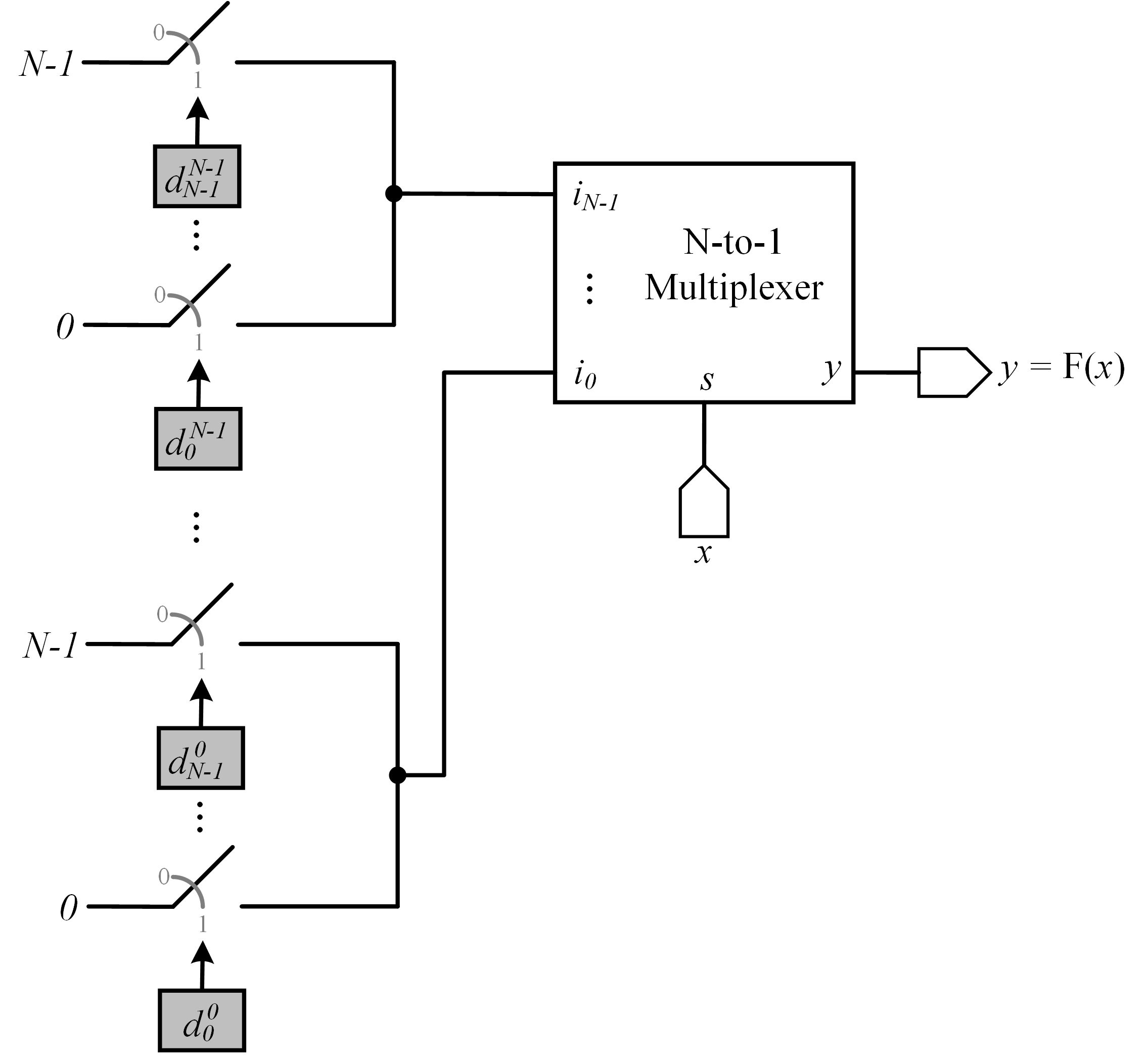
We will benefit from Nary multiplexers as our second option to implement multiple-valued logic functions. Therefore, we will start with defining the Nary multiplexer in this section. The multiplexer works such that one of its Nary inputs is connected to output via its Nary select pins. Therefore, we will first propose a -to-one multiplexer. While doing so, we will benefit from switches and one-to- decoder introduced in Section 3.1. Afterward, we will construct the -to-one multiplexer using -to-one multiplexers.
4.1 -to-One Multiplexer Formation
Symbolic representation of the Nary -to-one multiplexer with one select pin is as in Fig. 3. In this figure, for are N separate inputs, each being an Nary number. is the Nary select input. is Nary output of the multiplexer. We can form the input output relation of the -to-one multiplexer as
| (2) |
where are the decoded form of the select signal as explained in Section 3.1. To note here, only one will have logic level 1. Hence, we can construct the proposed multiplexer using switches and decoder as in Fig. 3.
4.2 -to-One Multiplexer Formation
We can form the -to-one multiplexer by using -to-one multiplexers, each having one select pin. We can explain this procedure on a simple ternary multiplexer with two select pins as in Fig. 4.
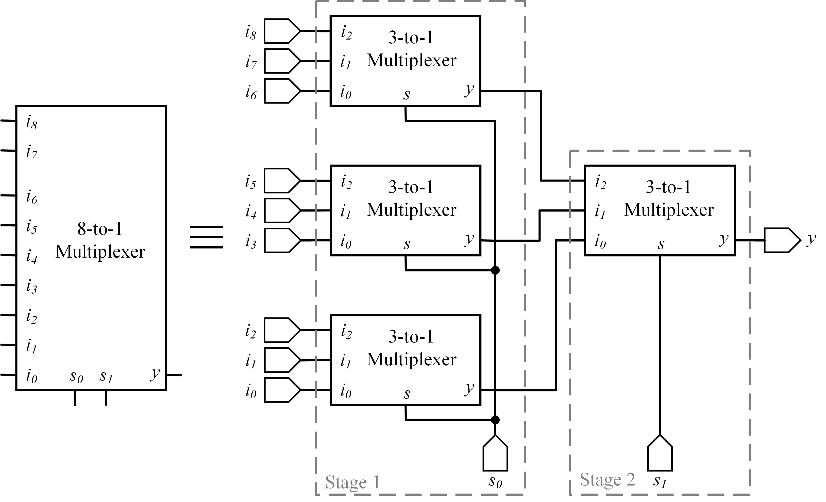
In Fig. 4, the first stage of the multiplexer has three three-to-one multiplexers, each controlled by the select pin . Output of the three multiplexers are fed to the second stage three-to-one multiplexer with the select pin . Thus, we need four three-to-one decoders in implementation. In general, we will need -to-one multiplexers to construct the -to-one multiplexer.
The -to-one multiplexer can also be constructed by switches and one -to- decoder. This is the direct extension of the method in Fig. 3. The reader can pick the suitable method for his or her own application.
5 Multiple-Valued Logic Function Realizations
We can realize any multiple-valued logic function by Nary decoders or multiplexers. We will consider each option separately in this section.
5.1 Nary Decoder based Realization
We can realize a multiple-valued logic function by Nary decoders introduced in Section 3. To do so, we should first form truth table of the function. Then, we should group inputs yielding the same output. Afterward, we should generate a control signal by applying binary OR operation to the corresponding decoder outputs. These control signals are then used to connect the appropriate Nary value to output.
Let’s consider the multiple-valued logic function to explain the procedure proposed in this section. We can decode the Nary input as for by our Nary decoder. We should apply binary OR to s producing the same output depending on the truth table of . Output of each OR gate will be the control signal for . These control signals are then used to connect the appropriate Nary value to output. We can mathematically represent this operation as
| (3) |
We can implement this structure as in Fig. 5. As can be seen in this figure, there is no sum term in the implementation of Eqn. 3. The reason for this is that, actually only one control signal will be at logic level 1 at a time. Hence, only one of will be fed to output.
The structure introduced in the previous paragraph can be extended to multiple-valued logic functions with inputs as . The only difference here will be the usage of an -to- decoder in operation. The number of control signals will be since we will have the output in Nary logic.
We can take the ternary half-adder as an example of multiple-valued logic function. Let’s realize it by the procedure introduced in this section. Therefore, we should first tabulate truth table of the half-adder as in Table 3. In this table, and are the two ternary numbers to be added. values are outputs of the two-to-nine decoder. The and terms represent the ternary sum and carry terms, respectively.
| 0 | 0 | 1 | 0 | 0 | 0 | 0 | 0 | 0 | 0 | 0 | 0 | 0 |
| 0 | 1 | 0 | 1 | 0 | 0 | 0 | 0 | 0 | 0 | 0 | 1 | 0 |
| 0 | 2 | 0 | 0 | 1 | 0 | 0 | 0 | 0 | 0 | 0 | 2 | 0 |
| 1 | 0 | 0 | 0 | 0 | 1 | 0 | 0 | 0 | 0 | 0 | 1 | 0 |
| 1 | 1 | 0 | 0 | 0 | 0 | 1 | 0 | 0 | 0 | 0 | 2 | 0 |
| 1 | 2 | 0 | 0 | 0 | 0 | 0 | 1 | 0 | 0 | 0 | 0 | 1 |
| 2 | 0 | 0 | 0 | 0 | 0 | 0 | 0 | 1 | 0 | 0 | 2 | 0 |
| 1 | 1 | 0 | 0 | 0 | 0 | 0 | 0 | 0 | 1 | 0 | 0 | 1 |
| 2 | 2 | 0 | 0 | 0 | 0 | 0 | 0 | 0 | 0 | 1 | 1 | 1 |
Based on Table 3, we can form and . Here, the binary OR operation is represented by the sign. Therefore, we can apply the binary OR operation to as the first group for the term to generate . Likewise, we can apply the binary OR operation to as the second group for the term to obtain . Finally, we can apply the binary OR operation to as the third group for the term to get . Hence, our control signals will be , , and for the ternary outputs 0, 1, and 2, respectively. Then, we can benefit from the structure as in Fig. 5 to realize the term of the half adder. In a similar manner, we can form the control signal for the term and realize it by another structure.
5.2 Nary Multiplexer based Realization
We can use the Nary multiplexer introduced in Section 4 to realize a multiple-valued logic function. As in the binary logic case, we should feed function values as input to the Nary multiplexer. Inputs of the function are connected to select pins of the multiplexer. Then, we will get output of the function from the multiplexer output.
As in the previous section, we can take the ternary half-adder as an example of the multiple-valued logic function. Let’s consider its realization by Nary multiplexers. Since the half adder has two ternary inputs, we should use two separate nine-to-one multiplexers for the and terms. Let’s consider realization of the term first. Here, we will have inputs of the Nary multiplexer as based on Table 3. Select pins of the multiplexer will be connected to inputs of the function and . Then, output of the first multiplexer can be taken as the term. We can follow the same steps by using a second multiplexer to form the term.
6 Adding Reconfigurability to the Multiple-Valued Logic Function Realizations
The Nary decoder introduced in Section 3 has binary output. Therefore, we can use binary D-latches in connection with decoder outputs for reconfigurable multiple-valued logic function realization. We can benefit from D-latches in a similar manner for the multiplexer based reconfigurable function realization. We will consider each option next.
6.1 Nary Decoder based Reconfigurable Function Realization
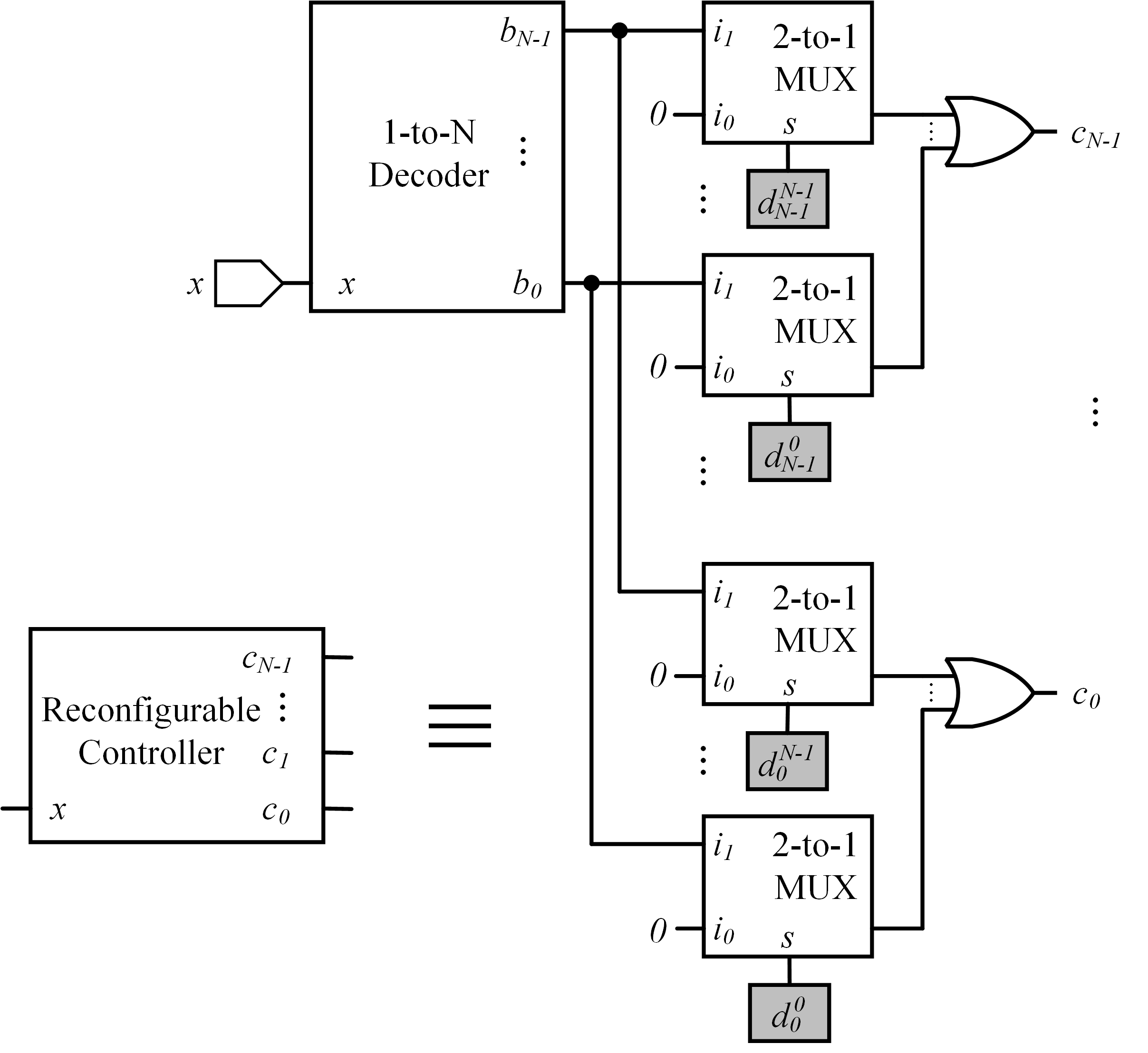
We should add latches between the decoder and control signals to add reconfigurability to the Nary decoder based multiple-valued logic function realization. Moreover, each control signal should have all decoder inputs for reconfigurability. Hence, our control signal representation for the Nary function with one input will be for , where is the D-latch output for the th control signal with input . Here, we have the binary OR operation represented by the sum symbol. We can reconfigure the proposed structure by setting appropriate D-latch values to logic level 0 or 1. We will have a setup as in Fig. 6 in hardware form.
6.2 Nary Multiplexer based Reconfigurable Function Realization
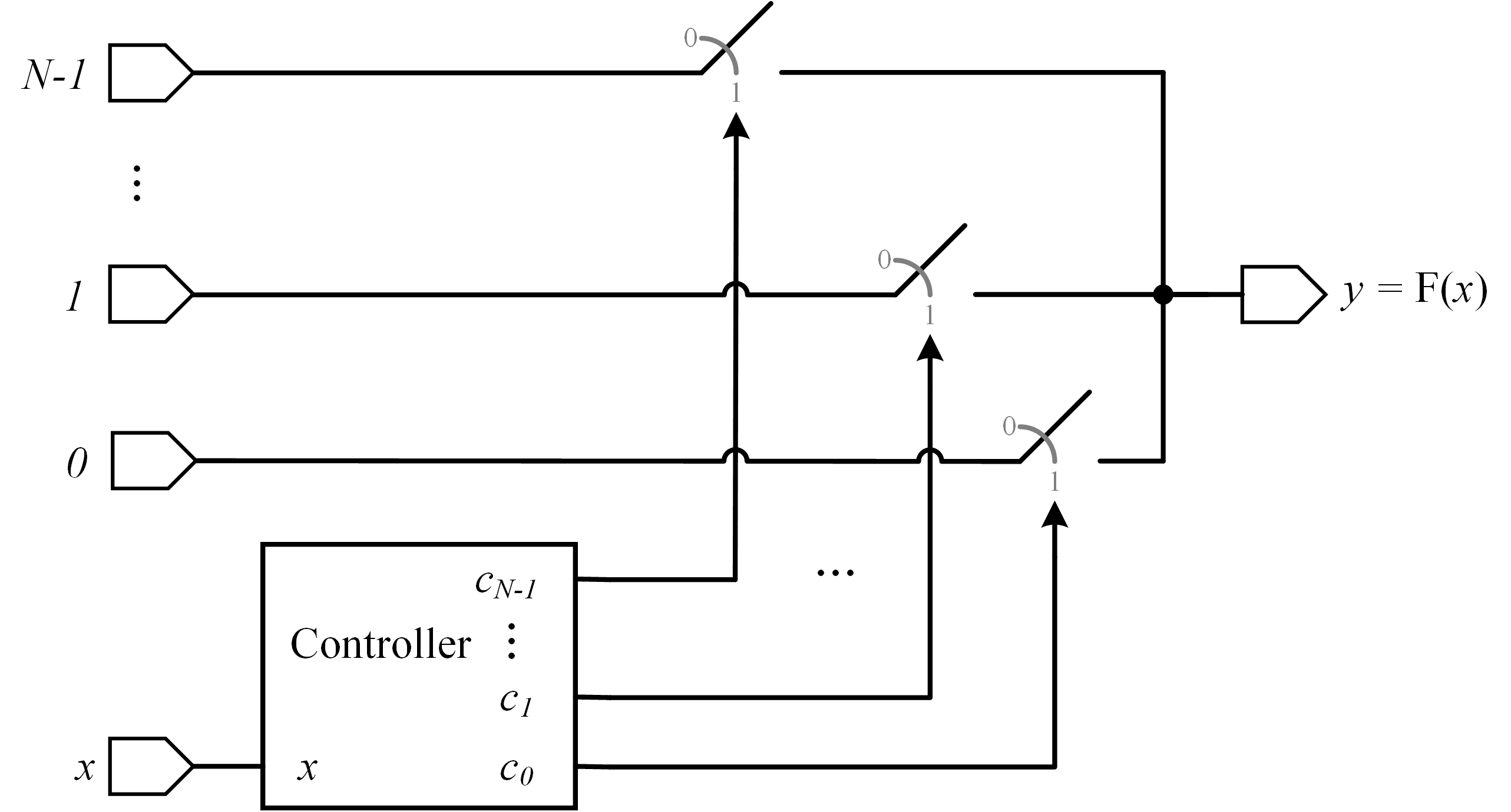
We can use Nary multiplexers to realize reconfigurable Nary functions. To do so, we should add Nary selection blocks before each input of the Nary multiplexer as in Fig. 7. Therefore, th input of the multiplexer will be formed as for , where are output of binary latches. We can reconfigure the structure by feeding logic level 0 or 1 to the corresponding D-latch input for reconfigurability.
7 Multiple-Valued Sequential Circuit Realization
In this section, we cover Nary sequential circuits. First, we propose the Nary D-latch. Then, we will use it along with the Nary function realization introduced in Section 5 to form Nary sequential circuits.
7.1 Nary D-Latch
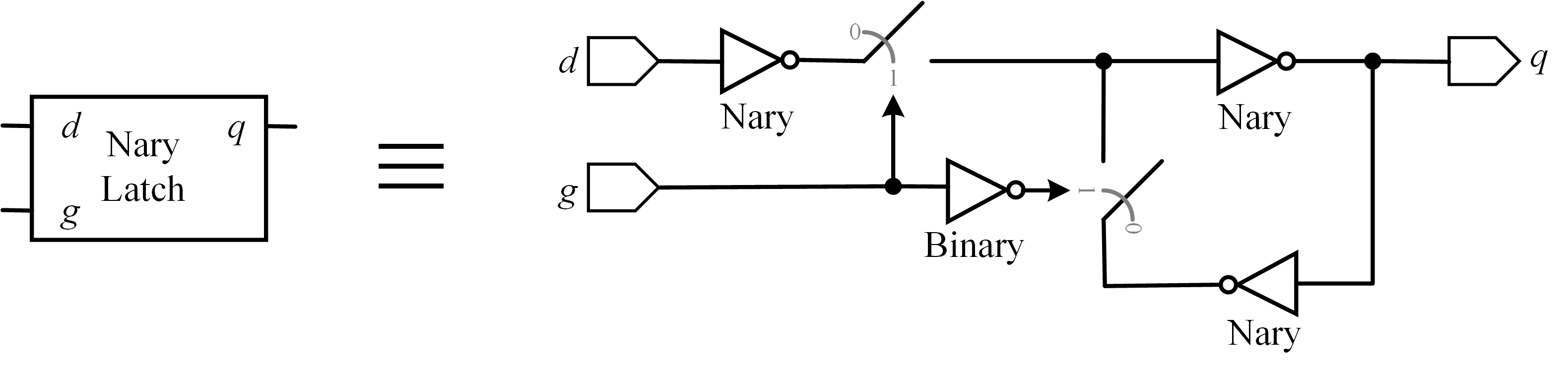
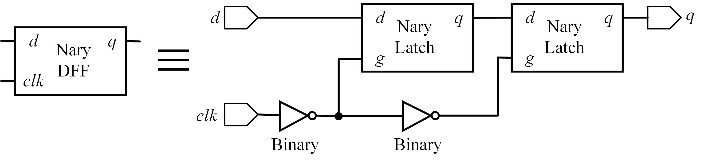
We can form an Nary D-latch by realizing the formula where and stand for the data and gate pins, respectively. is the output of the Nary D-latch. is the last value stored in the latch. When , the output will keep its previous value. When the output will be set to the value at the data pin . We can implement the proposed Nary latch by Nary and binary inverters and switches as in Fig. 8(a). If the input value to an Nary inverter is , then its output will have the value . The Nary inverter can be realized via one of the methods introduced in Section 5. An Nary D flip-flop can be implemented by cascading two D-latches as in Fig. 8(b).
7.2 Multiple-Valued Sequential Circuit Implementation
As we have the Nary function realization procedure and D flip-flop, we can extend the binary sequential circuit design procedure for the Nary case.
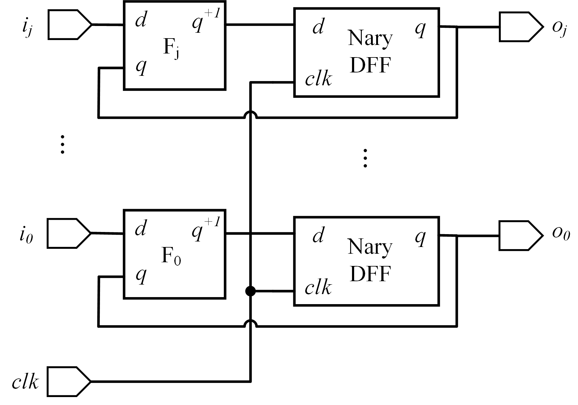
We can use the Nary D flip-flop and function realizations to construct sequential circuits. In general, next states is calculated from the present states and inputs as . The setup is shown in Fig. 9.
8 Final Comments
Utilization of TLG and multi-valued logic reduces power consumption and wire congestion. In this paper we introduced a general methodology to implement TLG based reconfigurable circuits. Proposed methodology may be used to build any reconfigurable multi-valued function. Modern digital designs heavily rely on design automation tools. However, similar tools are lacking for multi-valued logic designs. Development of these automation tools is a critical and open research field.
References
- [1] Maksim Andreev, Seunghwan Seo, Kil-Su Jung, and Jin-Hong Park. (2022). Looking beyond 0 and 1: principles and technology of multi-valued logic devices. Advanced Materials, 34(51):2108830.
- [2] Andrew Boutros and Vaughn Betz. (2021). Fpga architecture: Principles and progression. IEEE Circuits and Systems Magazine, 21(2):4–29.
- [3] Diogo Brito, Taimur G Rabuske, Jorge R Fernandes, Paulo Flores, and José Monteiro. (2014). Quaternary logic lookup table in standard cmos. IEEE Transactions on very large scale integration (vlsi) systems, 23(2):306–316.
- [4] Sumanta Chaudhuri. (2018). Beyond bits: A quaternary fpga architecture using multi-vt multi-vdd fdsoi devices. In 2018 IEEE 48th International Symposium on Multiple-Valued Logic (ISMVL), pages 38–43. IEEE.
- [5] Ricardo C Goncalves da Silva, Cristiano Lazzari, Henri Boudinov, and Luigi Carro. (2009). Cmos voltage-mode quaternary look-up tables for multi-valued fpgas. Microelectronics Journal, 40(10):1466–1470.
- [6] Pierre-Emmanuel Gaillardon, Xifan Tang, Gain Kim, and Giovanni De Micheli. (2014). A novel fpga architecture based on ultrafine grain reconfigurable logic cells. IEEE Transactions on very large scale Integration (VLSI) Systems, 23(10):2187–2197.
- [7] Patrick WC Ho, Haider Abbas F Almurib, and T Nandha Kumar. (2017). Configurable memristive logic block for memristive-based fpga architectures. Integration, 56:61–69.
- [8] Kotb Jabeur, Natalya Yakymets, Ian O’Connor, and Sébastien Le-Beux. (2011). Fine-grain reconfigurable logic cells based on double-gate cntfets. In Proceedings of the 21st edition of the great lakes symposium on Great lakes symposium on VLSI, pages 19–24.
- [9] Cristiano Lazzari, Paulo Flores, José Monteiro, and Luigi Carro. (2010). A new quaternary fpga based on a voltage-mode multi-valued circuit. In 2010 Design, Automation & Test in Europe Conference & Exhibition (DATE 2010), pages 1797–1802. IEEE.
- [10] Hadi Parandeh-Afshar, Hind Benbihi, David Novo, and Paolo Ienne. (2012). Rethinking fpgas: elude the flexibility excess of luts with and-inverter cones. In Proceedings of the ACM/SIGDA international symposium on Field Programmable Gate Arrays, pages 119–128.
- [11] Shubham Rai, Pallab Nath, Ansh Rupani, Santosh Kumar Vishvakarma, and Akash Kumar. (2021). A survey of fpga logic cell designs in the light of emerging technologies. IEEE Access, 9:91564–91574.
- [12] Jingxiang Tian, Gaurav Rajavendra Reddy, Jiajia Wang, William Swartz, Yiorgos Makris, and Carl Sechen. (2017). A field programmable transistor array featuring single-cycle partial/full dynamic reconfiguration. In Design, Automation & Test in Europe Conference & Exhibition (DATE), 2017, pages 1336–1341. IEEE.
- [13] Ahmet Unutulmaz and Cem Ünsalan. (2024). Implementation and applications of a ternary threshold logic gate. Circuits, Systems, and Signal Processing, 43(2):1192–1207.
- [14] Ankit Wagle and Sarma Vrudhula. (2021). Heterogeneous fpga architecture using threshold logic gates for improved area, power, and performance. IEEE Transactions on Computer-Aided Design of Integrated Circuits and Systems, 41(6):1855–1867.
- [15] Stephen M Williams and Mingjie Lin. (2018). Architecture and circuit design of an all-spintronic fpga. In Proceedings of the 2018 ACM/SIGDA International Symposium on Field-Programmable Gate Arrays, pages 41–50.