Synaptogen: A cross-domain generative device model for large-scale neuromorphic circuit design
Abstract
We present a fast generative modeling approach for resistive memories that reproduces the complex statistical properties of real-world devices. To enable efficient modeling of analog circuits, the model is implemented in Verilog-A. By training on extensive measurement data of integrated 1T1R arrays (6,000 cycles of 512 devices), an autoregressive stochastic process accurately accounts for the cross-correlations between the switching parameters, while non-linear transformations ensure agreement with both cycle-to-cycle (C2C) and device-to-device (D2D) variability. Benchmarks show that this statistically comprehensive model achieves read/write throughputs exceeding those of even highly simplified and deterministic compact models.
circuit modeling, statistics, neural network hardware, stochastic circuits, resistive circuits
1 Introduction
A pressing challenge for large-scale simulations of neuromorphic systems is the availability of suitable synaptic device models for resistive memories such as ReRAM [1]. For applications, it is important to capture the complex stochastic behavior of the devices, and models need to be fast enough to simulate millions of cells at once to handle modern neural network circuits. To this end, computationally lightweight generative models can be trained on electrical characteristics of fabricated devices, providing high speed simulations of large networks with unprecedented statistical accuracy [2].
While our previous work focused on large-scale simulations in high-level programming languages, here we present a circuit-level model implemented in the hardware description language Verilog-A, which is necessary to bridge the divide between the machine learning (ML) and analog circuit simulation domains. The model was expanded to cover a device configuration with access transistors (1T1R), and we introduce a measurement protocol for collecting the necessary training data on integrated memory arrays. The stochastic modeling approach closely captures the distributions, cross-correlations, and history dependence of ReRAM switching parameters as the devices are cycled (C2C), and has an extended treatment of how those statistics vary between the different devices on the chip (D2D). The resulting device model is far more statistically comprehensive than existing compact models and significantly outperforms them in read/write benchmarks for both independent devices and for crossbar arrays. In circuit simulations, we demonstrate weight programming and readout of crossbars with up to 256256 and 10241024 devices respectively, the feasibility of which has not been shown previously.
2 Methods
2.1 Electrical measurements
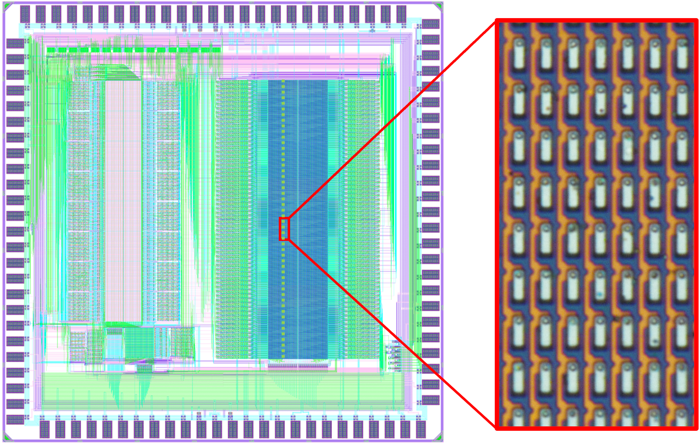
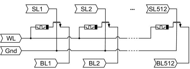
An integrated ReRAM chip was obtained through the manufacturing broker Circuits Multi-Projects (CMP) and used for electrical measurements. A 51232 1T1R crossbar array was part of a custom layout within the Memory Advanced Demonstrator 200mm (MAD200) design environment (Fig. 1). Select logic and access transistors were implemented in the HCMOS9A STMicroelectronics 130 nm CMOS process, and ReRAM devices with material stack TiN/HfO2/Ti were deposited in a post-process by CEA-LETI [3]. Each ReRAM device in the array is connected in series with an integrated common-source N-channel MOSFET in a standard 1T1R configuration. The 512 bit lines and corresponding select lines (SLs) are each internally multiplexed to single output pins, whereas the 32 word lines (WLs) are directly routed to individual pins. The packaged chip was mounted on a custom printed circuit board (PCB) providing a PC interface via the digital outputs of a USB data acquisition board whereby devices can be individually addressed for measurement. In this work, a total of 512 devices sharing a single WL in the array were sequentially selected to collect training data (Fig. 2).
High speed measurements were performed using external generating and sampling equipment connected to the PCB over 50 lines. In order to collect bipolar switching cycles continuously with a single driving signal, an unusual 1T1R biasing was necessary. The chip substrate (and FET body) was biased to -1.8 V relative to signal ground and the gate was biased to 1.35 V while a bipolar driving signal was applied to the WL and current was measured at the BL through a 50 shunt to 0 V. Devices were formed by a single 3 V amplitude 1 ms triangle pulse before being cycled by a continuous triangle waveform between -1.5 V and 2 V with 1 ms period. Preconditioning cycles were initially applied to each cell before collecting 6,000 switching current vs. voltage () traces for each of the 512 devices.
2.2 Statistical modeling
The core concept of the generative device model is to first extract important features (i.e. resistance and voltage threshold levels) from each cycle of the training data, then learn to efficiently generate new samples with very similar statistical properties. Using the generated features as a guide, we approximate the dependence for simulated cells according to the voltage sequence applied to them.
2.2.1 Feature generation
The chosen features to model are extracted from the raw data and organized into vector time series
| (1) |
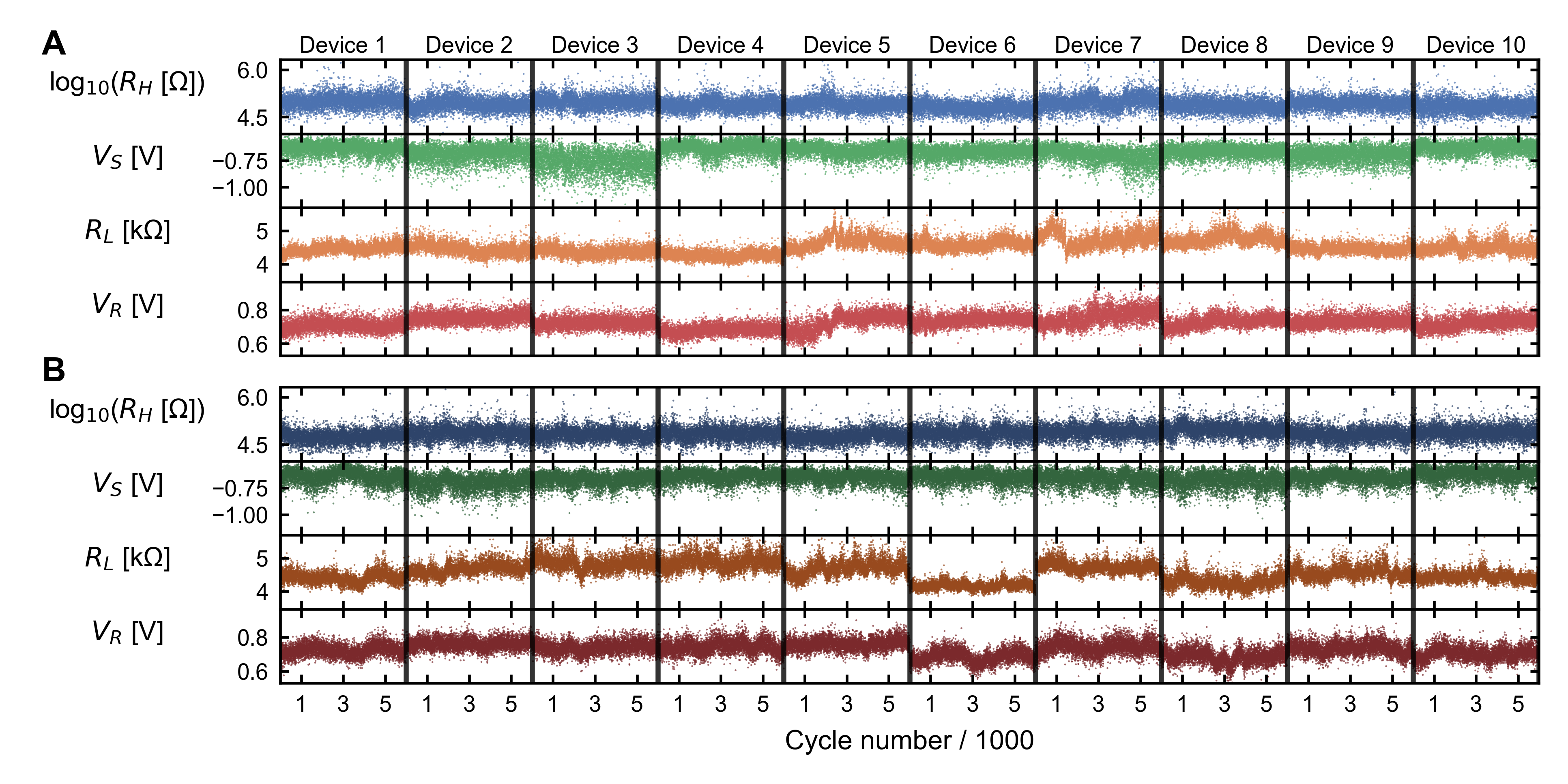
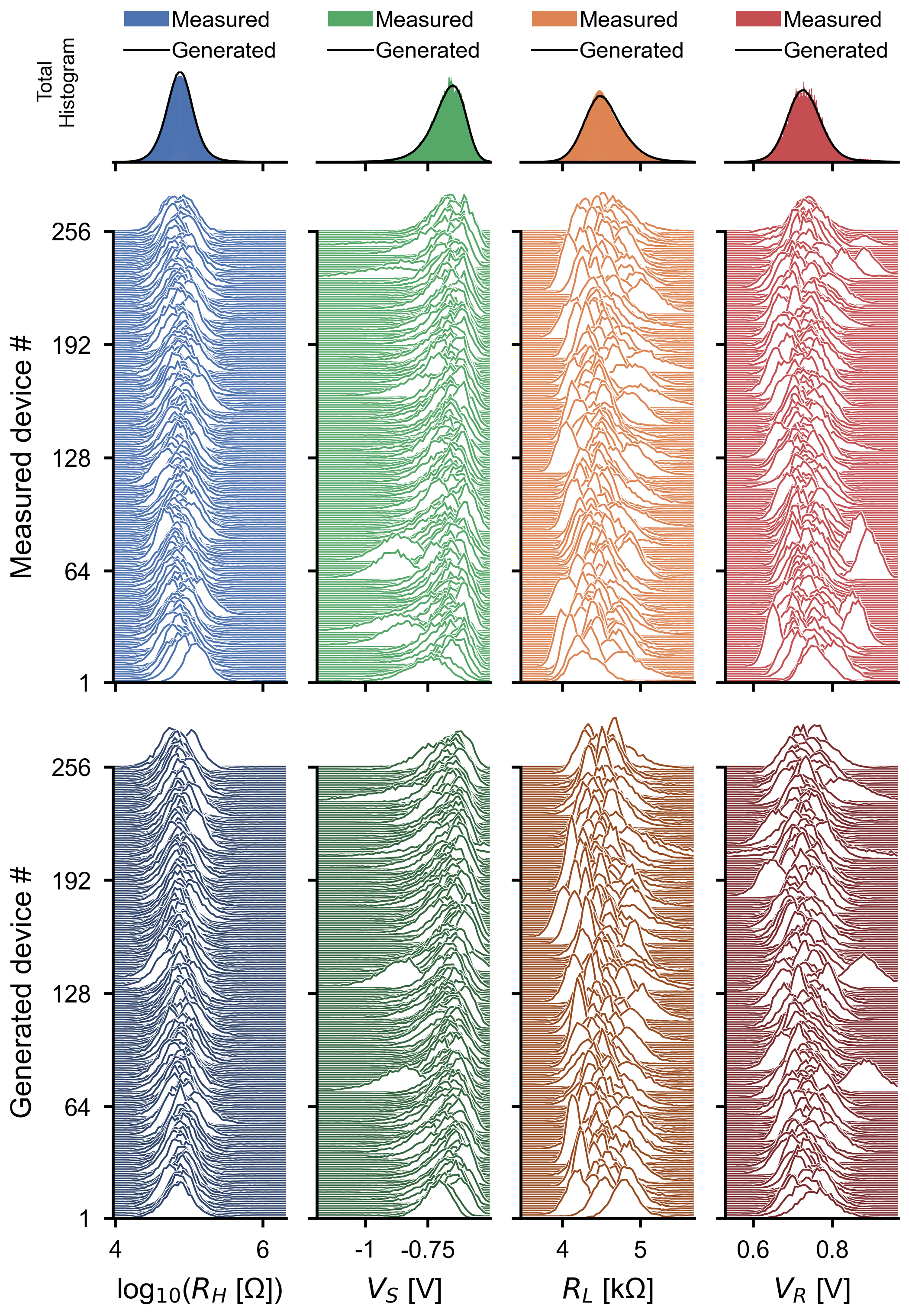
for each cycle number and device number . The feature vectors are arranged from top to bottom in the order that they occur in the measurement; is the resistance of the high resistance state (HRS), is the voltage of the SET transition, is the resistance of the low resistance state (LRS), and is the voltage at the start of the RESET transition. The details of this feature extraction are documented in [2].
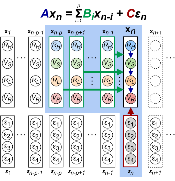
Feature vector generation is based on a discrete vector autoregressive (VAR) stochastic process (Fig. 3), which captures the cycle history dependence and the correlations between features [4]. A VAR() models the th feature vector as a linear function of past values within cycle range and is driven by 4-dimensional white noise . The stochastic process has the easily computable form,
| (2) |
where , , and are weight matrices subject to training.
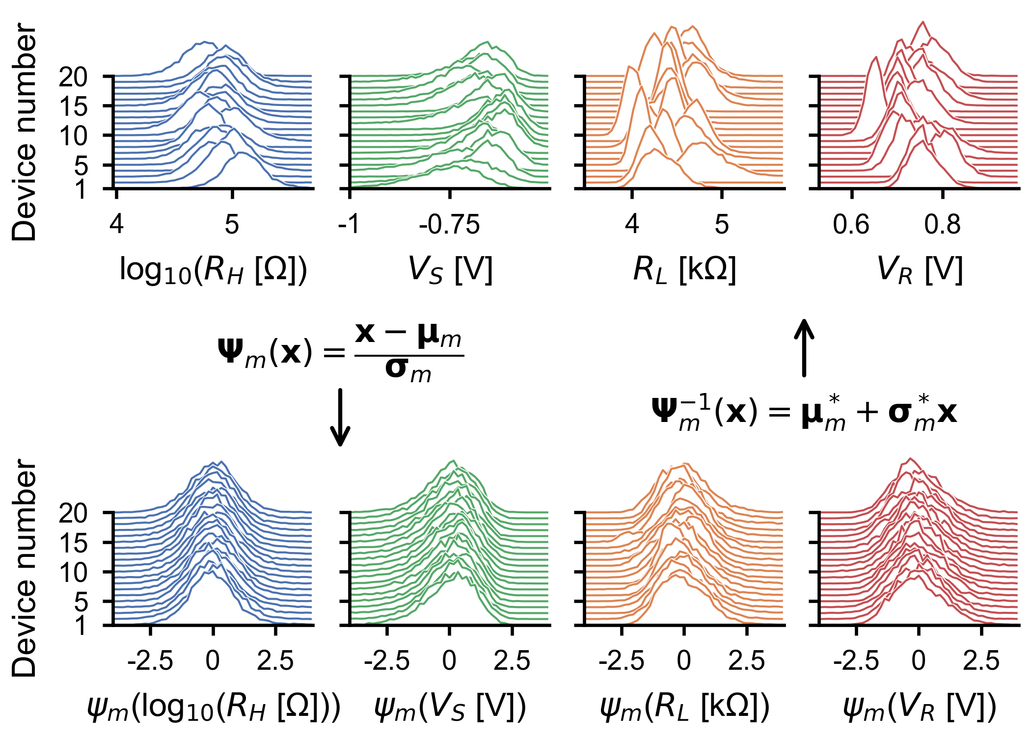
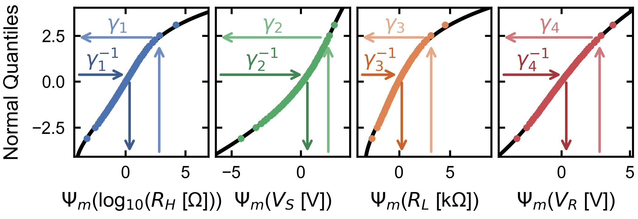
To map the normally distributed output of the VAR process to the joint empirical distribution measured across cycles and across devices, we apply a sequence of invertible transformations. The parameters of these transformations are learned in a single training pass in which the generative process is carried out in reverse (Fig. 4). Thereby, the marginal distributions of the extracted features are normalized in two steps. First, the device-specific mean and variance over the sampled cycles are standardized using an affine transformation (Fig. 5). Then, to further shape the intermediate probability densities into normal distributions, the affine transformation is followed by a parameterized, non-linear quantile transform . A VAR() process is then fit to the normalized data using least squares regression.
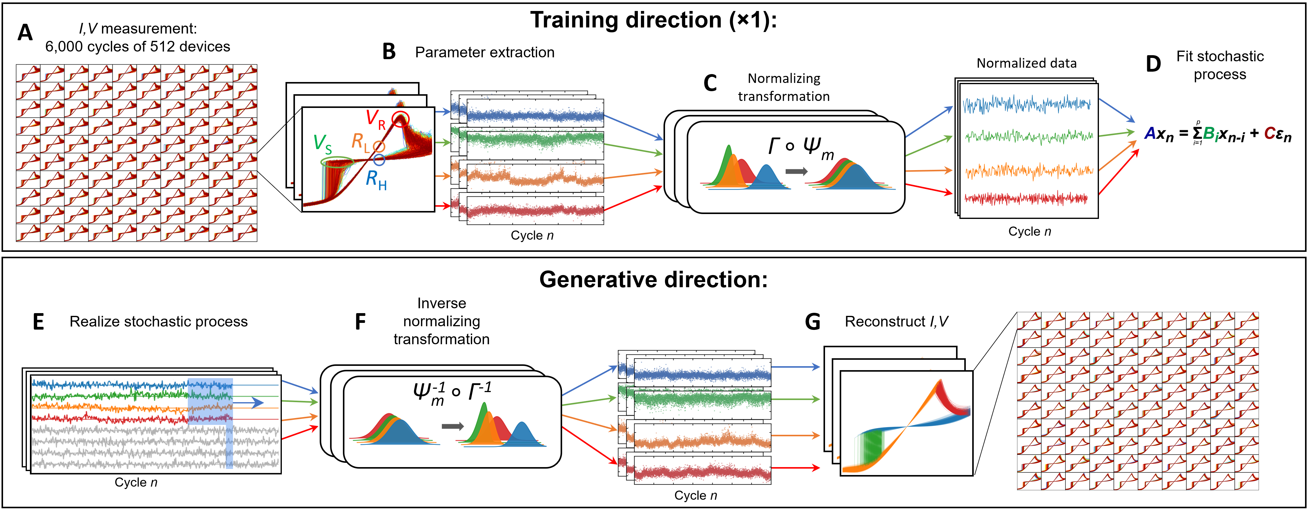
In the generative direction, the learned transformations are inverted and applied to independent realizations of the VAR process for each simulated device. The normalizing map is defined such that its inverse consists of element-wise polynomial evaluations,
| (3) |
where are 4th degree polynomials and are visualized in Fig. 6.
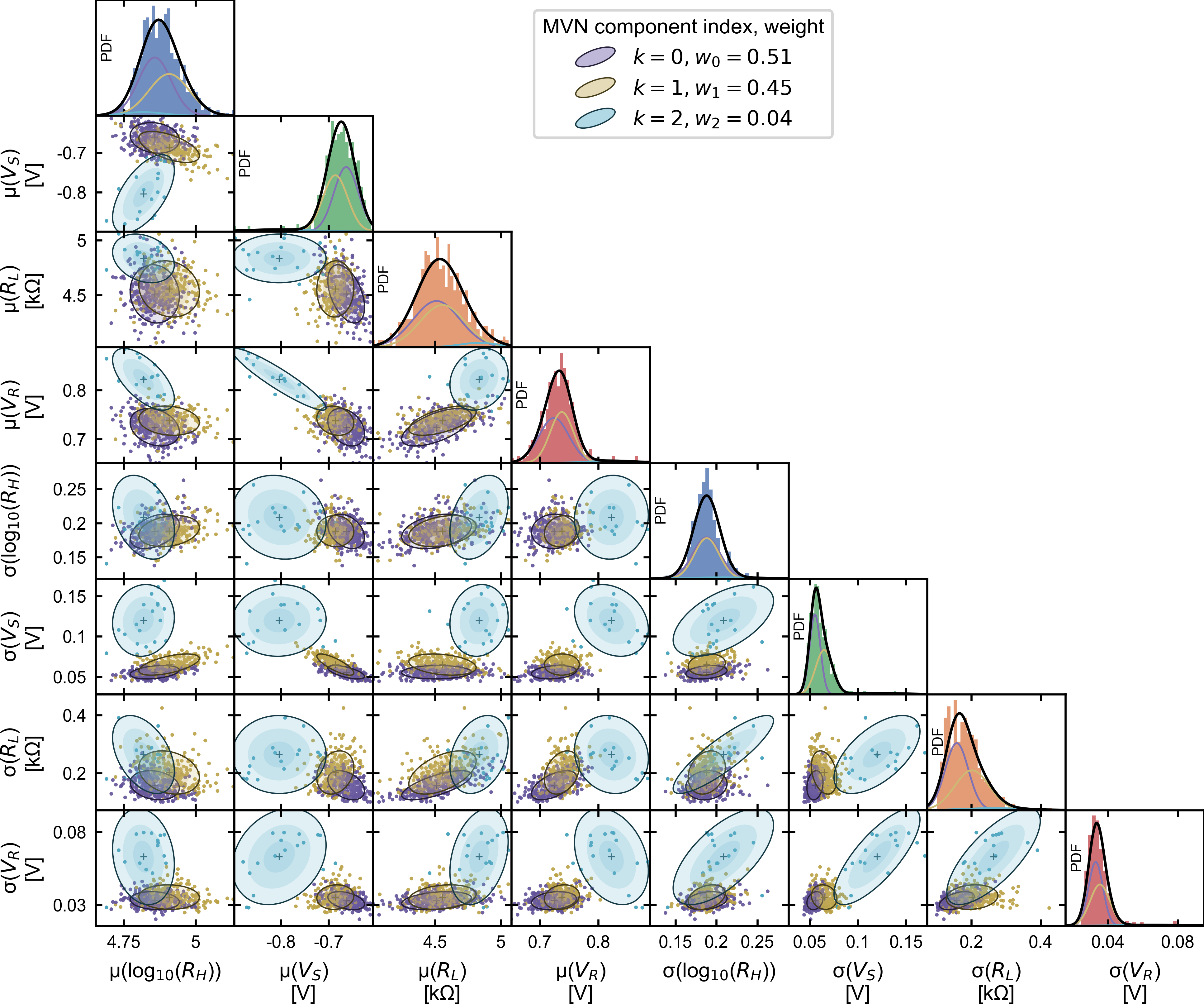
To restore device-specific offsets and scales to the generated features, we invert by approximating the distribution of an 8-dimensional block vector of sampled C2C means () and standard deviations (),
| (4) |
This distribution is represented by a superposition of multivariate normal (MVN) distributions, which is known as a Gaussian mixture model (GMM). A GMM is cheap to sample from and allows a close fit of the covariance structure of the main cluster of datapoints. The GMM also captures the structure of statistical abnormalities that occur (i.e. defective devices), which may have a disproportionate impact on system performance. A three-component GMM, denoted
| (5) |
is fit to the empirical distribution by the expectation–maximization algorithm using k-means initialization and is visualized in Fig. 7.
2.2.2 Modeling the dependence
The non-linear state for each cell is modeled as a linear combination of two static, global limiting polynomials and (degree 5 and 6 respectively), whose coefficients are estimated from the training data. This way, the model can reproduce a wide variety of asymmetric non-linearities in both high and low resistance states, and can also absorb the non-linearity of series transistors when trained on 1T1R data.
Resistance levels of the devices are tracked by continuous state variables , which represent the degree of mixing between the pre-defined limiting polynomials. The current as a function of voltage for device assumes the form
| (6) |
The state variable corresponding to each generated resistance level is calculated using the function
| (7) |
which uniquely sets the static resistance of the device (evaluated at V) equal to .
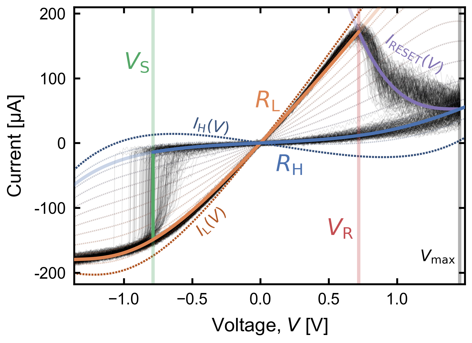
Transitions of the state variables occur when the voltage applied to a device exceeds the threshold levels for SET or RESET in its current cycle. The transitions connect each generated resistance state to the following one, as illustrated in Fig. 8. Below the SET threshold , there is an instantaneous transition from resistance state to . After SET has occured, voltages above gradually shift the resistance state from to . This gradual RESET proceeds such that the device current has an empirical functional form
| (8) |
where
| (9) | ||||
| (10) |
is the maximum voltage applied in the experimental sweeps, and the constant sets the curvature of the RESET transition as estimated by a least squares fit to the training data.
2.3 Implementation and benchmarks
By using easily evaluated polynomials and matrix multiplications throughout, Synaptogen is designed for high throughput and parallelization. We recently benchmarked an implementation in the Julia programming language, comparable with the present model in terms of speed, demonstrating the practicality of simulating large-scale physical neural networks with over weights [2]. However, due to the growing interest in simulating networks at the circuit level, efficient stochastic device models implemented in a hardware description language (HDL) are currently highly sought after [5, 6, 7, 8].
To suit a circuit design ecosystem and to compare speeds with alternative models, we implemented Synaptogen in the Verilog-A HDL. Special programming requirements were imposed by the adaptation to a transient model description and by the weak support for dynamic structures in Verilog-A. Furthermore, due to the discontinuities at the threshold voltages, the simulation step size was limited locally at each device threshold to aid convergence. The order of the VAR process in the Verilog-A implementation was fixed to .
Simulation speeds were compared with a minimalistic non-stochastic linear ion drift model (LinearDrift) as a baseline [9], as well as the more complex physics-based JART v1b variability-aware model [5]. Read speeds are also compared with randomly initialized arrays of ohmic resistances, a linearly solvable problem which gives an upper bound for the speed of the simulation framework.
We benchmarked the read and write performance for both parallel operation of independent cells as well as for crossbar arrays with resistive leads (5 between every circuit node). This distinction is important because lead resistance has a strong impact on the system, but is much slower to solve due to the strongly coupled equations [10, 11]. For the purpose of comparing simulation speeds between the independent-device and crossbar-connected cases, the same applied voltage waveform was shared by rows and columns of the independent devices as though they were connected by WLs and BLs. This makes the problem equivalent to a crossbar array with zero lead resistance, but in practice is significantly faster than enforcing crossbar connectivity in the netlist.
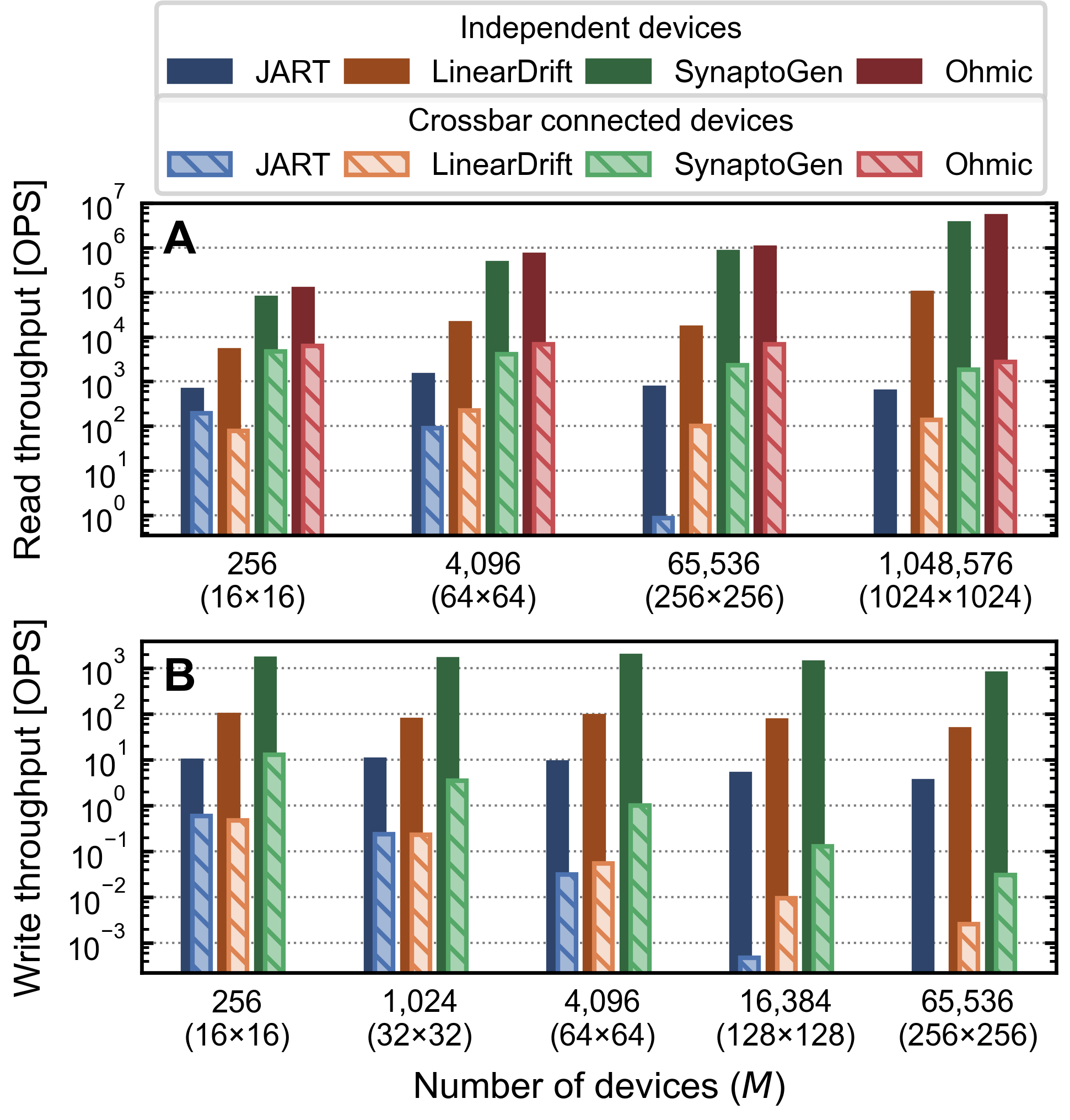
Simulations were performed using the Cadence Spectre simulator with “moderate” settings for both the “accelerated parallel simulator” (APS) and error tolerance, running on 8 (out of 18) cores of Intel Xeon Gold 6154 CPU. Square bipolar voltage pulses were applied to the WL terminals to simulate read/write operations, and the throughput in operations per second (OPS) was calculated as the number of devices involved in the read/write process divided by the total time taken for the transient analysis.
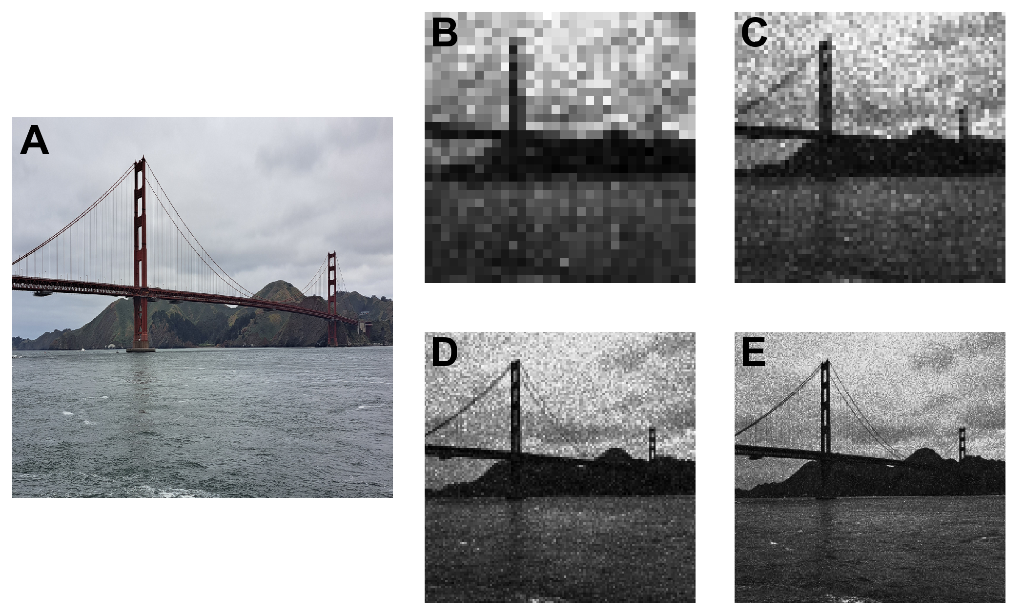
For weight programming benchmarks, arrays of devices were initialized in their LRS before writing grayscale image data into their resistance states by partial RESET (Fig. 9). The pixel values were linearly mapped to a suitable reset voltage range and, using a half-select voltage scheme [12], the voltages were sequentially applied to the corresponding cells for 1 \unit\micro. For situations where the entire array could not be written in a practical amount of time, the throughput was determined by writing a 16×16 sub-block of devices.
For readout benchmarks, 200 mV pulses were simultaneously applied to all WLs for 1 ns as current was measured at the grounded BL terminals. The results of the read and write benchmarks are summarized in Fig. 10.
3 Results
The described hierarchical modeling approach efficiently generates feature vectors that closely resemble the training data. This can be visually verified with respect to the time series behavior (Fig. 11). The correlated variations in the feature distributions across different devices are very closely replicated while simultaneously recreating the total distributions over all devices and cycles (Fig. 12).
For all models and conditions, read operations were significantly faster than writes, and speeds were much higher for independent devices than for an equal number of crossbar connected devices. Synaptogen wrote at OPS for independent devices, but started at 13 OPS for 1616 crossbars, degrading with crossbar size to only 0.3 OPS at 256256. For readout, Synaptogen is competitive with simple ohmic resistive networks, reaching 60% to 80% of their speed in most cases. The throughput of these read operations increased for larger numbers of devices, with OPS for 256 devices and OPS for 1,048,576 devices. Crossbar connected readouts were slowed by 2 to 4 orders of magnitude relative to independent devices as the array size increased from 1616 to 256256.
Synaptogen was between 10 and 100 faster than LinearDrift for all benchmarks, which is remarkable because LinearDrift is a very simple ordinary differential equation (ODE) formulation for which the simulator should be well adapted. Furthermore, LinearDrift does not include C2C or D2D variability, and cannot reproduce many important switching features of actual devices. Synaptogen even more significantly outperforms the JART v1b variability model, which is more closely comparable in terms of covered device behavior. Due to its complexity and implicit formulation, JART performance degrades faster than the other models as the array size grows; for JART array sizes 256256 and above, not even a single write operation could be performed in a reasonable time frame. At 10241024, read operations were also impossible. For the conditions that could be simulated, operations on independent Synaptogen devices were always over 100 faster, with the speed of writes approximately 200, and reads reaching 6,000 those of JART. For the resistive crossbar simulations, Synaptogen was between 10 to 100 faster for 6464 and smaller arrays, and between 100 and 10,000 for larger arrays.
Analog circuit simulations face intrinsic speed limitations due to the computation necessary at each time step to converge on solutions to large systems of non-linear differential equations. Even with dramatic speed increases over competing models, simulation in Cadence Spectre with Synaptogen synapses is practical for training and inference of fully connected neural network layers only within limits. Table 1 shows the time necessary to write a pre-trained model and to perform an inference operation according to our benchmarks. While many operations can be completed in well under a second, others (such as writing to large resistive crossbars) can take a considerable amount of time (hours or days).
As modern ML networks commonly exceed millions of weights, these benchmarks highlight the need to extend the device model’s applicability to larger scales. Therefore, while the Verilog-A implementation provides compatibility with circuit design tools, we also implemented Synaptogen in the Julia programming language. The internal operation is the same for both models, while the latter achieves orders of magnitude higher speed by avoiding transient calculations.
| Layer size | Weight Initialization | Inference | ||
|---|---|---|---|---|
| Independent | Crossbar | Independent | Crossbar | |
| 16×16 | 160 ms | 20 s | 3.4 ms | 54 ms |
| 32×32 | 660 ms | 4.9 min | ||
| 64×64 | 2.3 s | 1.1 h | 9.2 ms | 1.0 s |
| 128×128 | 13 s | 1.5 d | ||
| 256×256 | 1.4 min | 25 d | 82 ms | 28 s |
| 1024×1024 | 300 ms | 9.6 min | ||
4 Conclusion
In this work, we developed a generative compact model for resistive switching devices that seamlessly adapts to statistical measurements. Through an automated training procedure, the model closely captures both C2C and D2D variability of data measured on integrated ReRAM devices. While an equivalent model can be used in a high-level programming domain for larger scale simulations, here we demonstrate its use in analog circuit simulation of 1T1R arrays. The implemented circuit level model operates orders of magnitude faster for reading and writing compared to other compact models, and we demonstrate crossbar programming (256256 devices) and readout (10241024 devices) at scales which far exceed what was previously possible in the analog circuit simulation domain.
Code availability
The Verilog-A compact model as well as its Julia counterpart are available on GitHub (https://github.com/thennen/synaptogen) and archived in Zenodo (https://zenodo.org/doi/10.5281/zenodo.10942560).
References
- [1] C. Nail et al., “Understanding RRAM endurance, retention and window margin trade-off using experimental results and simulations,” in 2016 IEEE International Electron Devices Meeting (IEDM), San Francisco, CA, USA: IEEE, Dec. 2016, p. 4.5.1-4.5.4. doi: 10.1109/IEDM.2016.7838346.
- [2] T. Hennen et al., “A high throughput generative vector autoregression model for stochastic synapses,” Front. Neurosci., vol. 16, p. 941753, Aug. 2022, doi: 10.3389/fnins.2022.941753.
- [3] A. Grossi et al., “Fundamental variability limits of filament-based RRAM,” in 2016 IEEE International Electron Devices Meeting (IEDM), San Francisco, CA, USA: IEEE, Dec. 2016, p. 4.7.1-4.7.4. doi: 10.1109/IEDM.2016.7838348.
- [4] J. D. Hamilton, Time series analysis. Princeton, N.J: Princeton University Press, 1994.
- [5] C. Bengel et al., “Variability-Aware Modeling of Filamentary Oxide-Based Bipolar Resistive Switching Cells Using SPICE Level Compact Models,” IEEE Transactions on Circuits and Systems I: Regular Papers, vol. 67, no. 12, pp. 4618–4630, 2020, doi: 10.1109/TCSI.2020.3018502.
- [6] V. Ntinas et al., “A Simplified Variability-Aware VCM Memristor Model for Efficient Circuit Simulation,” in 2023 19th International Conference on Synthesis, Modeling, Analysis and Simulation Methods and Applications to Circuit Design (SMACD), Funchal, Portugal: IEEE, Jul. 2023, pp. 1–4. doi: 10.1109/SMACD58065.2023.10192107.
- [7] J. Reuben, M. Biglari, and D. Fey, “Incorporating Variability of Resistive RAM in Circuit Simulations Using the Stanford–PKU Model,” IEEE Trans. Nanotechnology, vol. 19, pp. 508–518, 2020, doi: 10.1109/TNANO.2020.3004666.
- [8] S. Guitarra, P. Mahato, D. Deleruyelle, L. Raymond, and L. Trojman, “Stochastic based compact model to predict highly variable electrical characteristics of organic CBRAM devices,” Solid-State Electronics, vol. 185, p. 108055, Nov. 2021, doi: 10.1016/j.sse.2021.108055.
- [9] S. Kvatinsky, E. G. Friedman, A. Kolodny, and U. C. Weiser, “TEAM: ThrEshold Adaptive Memristor Model,” IEEE Trans. Circuits Syst. I, vol. 60, no. 1, pp. 211–221, Jan. 2013, doi: 10.1109/TCSI.2012.2215714.
- [10] A. Chen, “A Highly Efficient and Scalable Model for Crossbar Arrays with Nonlinear Selectors,” in 2018 IEEE International Electron Devices Meeting (IEDM), San Francisco, CA: IEEE, Dec. 2018, p. 37.2.1-37.2.4. doi: 10.1109/IEDM.2018.8614505
- [11] D. Joksas and A. Mehonic, “badcrossbar: A Python tool for computing and plotting currents and voltages in passive crossbar arrays,” SoftwareX, vol. 12, p. 100617, Jul. 2020, doi: 10.1016/j.softx.2020.100617.
- [12] A. Chen, “Analysis of Partial Bias Schemes for the Writing of Crossbar Memory Arrays,” IEEE Trans. Electron Devices, vol. 62, no. 9, pp. 2845–2849, Sep. 2015, doi: 10.1109/TED.2015.2448592.