Proximity-Induced Exchange Interaction: a New Pathway for Quantum Sensing using Spin Centers in Hexagonal Boron Nitride
Abstract
Defects in hexagonal boron nitride (hBN), a two-dimensional van der Waals material, have raised wide range interest for its potential in various quantum applications. Due to hBN’s 2D nature, spin center in hBN can be engineered in close proximity to target material, providing advantages over their 3D counterparts, such as nitrogen-vacancy (NV) center in diamond. Here we propose a novel quantum sensing protocol driven by exchange interaction between spin center in hBN and the underlying magnetic substrate induced by magnetic proximity effect. By first-principle calculation, we demonstrate the induced exchange interaction dominates over dipole-dipole interaction by orders of magnitude when in proximity. The interaction remains antiferromagnetic across all stacking configuration between the spin center in hBN and the target van der Waals magnets. Additionally, we explored the scaling behavior of the exchange field as a function of the spatial separation between the spin center and the targets.
For Table of Contents Only
![[Uncaptioned image]](/html/2404.05208/assets/TOC.jpg)
Quantum sensing based on solid-state platform has been successful in delivering high resolution and stable measurements of various physical quantities such as temperature, pressure, strain, magnetic, electric, and even gravitational fields [1, 2, 3, 4]. High-precision, high-spatial resolution detection of magnetic fields is particularly important because it enables detailed understanding of physical phenomena ranging from fundamental quantum mechanics to many intricate biological processes [5, 6, 7, 8, 9]. Among the candidate platforms for probing magnetic field, color centers with particular spin and optical interface suitable for manipulation have been extensively investigated [10, 11, 12]. Current sensing applications predominantly rely on Zeeman interaction between the color center spins and the small stray field generated by the sensing target. Such Zeeman splitting is in the microwave range and usually measured by optically detected magnetic resonance (ODMR).
One widely used color center is the NV center in diamond [5, 13, 14, 15]. Despite its success, the NV center suffers from several intrinsic limitations. Firstly, high quality NV centers are usually embedded in the diamond bulk, as it is difficult to obtain NV center with long coherence time near diamond surface due to the noise from surface dangling bonds or loss of desirable charge state [16, 17]. This bulk embedment simultaneously impedes the ability to probe the sensing target at extreme proximity for atomic resolution. Furthermore, the magnetic sensing capabilities of NV centers are constrained by their inability to detect the magnetism of underlying targets with net zero magnetic moments, like antiferromagnetic (AFM) materials, which results in a vanishing stray field signal, excluding their use as in situ sensors for such applications. Secondly, Zeeman interaction splitting is determined by the projection of stray field to the quantization axis of color center. If the stray field is orthogonal to the quantization axis, there will be no signal on the ODMR spectrum. Thus, single NV center is only sensitive to the variation of stray field along the pre-determined quantization axis. These limitations mentioned above are generic for color centers embedded in bulk semiconductors.
A material platform that supports a fundamentally new sensing paradigm could be provided by defects in hexagonal boron nitride (hBN) [18, 19, 20, 21, 22, 23, 24, 25, 26] , a two-dimensional (2D) van der Waals (vdW) material. 2D vdW materials can be engineered to atomically thin layer while free from dangling bonds [27, 28]. This effectively resolves the two limitations we encounter with color centers in bulk semiconductors. The integration of 2D vdW materials into heterostructures facilitates the engineering of defects within a few layers from the interface with target sample, providing an opportunity for a new paradigm of ultrasensitive, in situ quantum sensing [29].
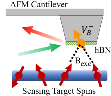
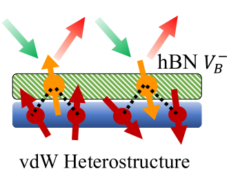

In this letter, we propose a novel quantum sensing protocol driven by the exchange interaction between spin center in 2D vdW material and the target sample, demonstrated in Fig. 1. Our ab-initio calculations demonstrate a gigantic exchange interaction on the order of meV between the negatively charged boron-vacancy () center and a magnetic substrate when engineered to proximity in a heterostructure. Remarkably, the strength of such exchange interaction remains robust across all stacking configurations, and dominates over classical dipole-dipole or stray-field interactions. Our proposal addresses obstacles encountered with stray-field based sensing protocol. This work thus introduces a new exchange interaction-driven in situ quantum sensing scheme with potential for ultrahigh sensitivity.
I Results and Discussion
I.1 Sensing Design
hBN hosts a variety of optically addressable defects that remain robust at room temperature and pressure [18, 30, 31, 32, 33, 34, 22, 35]. The negatively charged boron-vacancy () in hBN attracts particular interest due to its maturity in fabrication process and depth of research into its electronic and optical properties. Many recent studies have demonstrated the ability to initialize, manipulate, and readout the spin state of [20, 21, 23, 36, 37]. Since its first experimental report, quantum sensing application has spanned among static magnetic field, temperature, strain, pressure, and spin fluctuation [24, 25, 26, 38, 39, 40]. In this work, we will primarily focus on as the quantum sensors.
We start by outlining two general design principles of quantum sensing based on proximity-induced exchange interactions. First, the quantum sensor, i.e., the spin center, has to be structurally and electronically stable. This requires no covalent or ionic chemical bonds, or charge transfer between the desirable spin center and the sensing target, shown in Fig. 1c. To this end, we identified several 2D magnetic semiconductors, such as CrI3, , and CrSBr, as the sensing target of current interests, due to their technical importance [41, 42, 43, 44, 45] and compatibility with the center.
The second design principle of proximity quantum sensing is a significant exchange interaction between the quantum sensor and target, which causes measurable changes in the electronic structures of the quantum sensors. The center features a spin triplet ground state with a total magnetic moment of . The exchange interaction will split the and spin states within the ground state manifold, which could be measured by experiment such as optically detected magnetic resonance. Upon forming a vdW interface, we expect the exchange interaction between the and the 2D magnetic semiconductors, such as CrI3, to be comparable in size to the pairwise exchange interactions between adjacent magnet layers. In addition, the robustness of our proposed sensing scheme is ensured by the dominance of such significant exchange interaction over other interactions such as dipole-dipole interaction.
Potential experimental realizations of this novel quantum sensing protocol include direct integration of the spin center with an atomic force microscopy cantilever to scan the sensing target at proximity, as shown in Fig. 1a. The hBN sheets containing spin center could be coated onto the surface of atomic force microscopy cantilever. Alternatively, one can incorporate center and the sensing target into a vdW heterostructure, depicted in Fig. 1b, with existing technology such as optically detected magnetic resonance (ODMR) for measurement purpose. The inherent 2D nature adds extra flexibility in experimental setup, allowing for the adaptation of the hBN sheet onto various surfaces.

I.2 Band Alignment
Since center is negatively charged, electron transfer between center to the sensing target can lead to change of charge state and eventually the instability of the spin center. To satisfy the first design principle and ensure the the stability of center, it is imperative to avoid a type-III (or broken-gap) band alignment between the sensing target and center. In the type-III configuration, the highest occupied molecular orbital (HOMO) of center overlaps with or exceeds the lowest unoccupied molecular orbital (LUMO) of the sensing target, or vice versa. This would suggest an alternative electronic ground state other than the desired state. Fig. 1c shows an example of preferred band alignment between the sensing target and center.
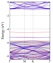
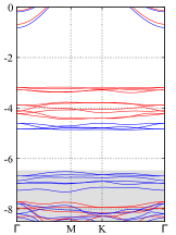
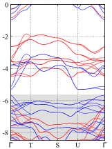
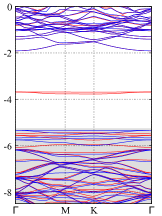
We expect proper band alignment to serve as a baseline requirement on selecting specific candidate sensing targets. As shown in Fig. 2, band structure calculations are carried out for and candidate monolayer target magnets including CrI3, , and CrSBr. The band energies are defined relative to vacuum level. In the case of , the vacuum level of this stand-alone charged defect is not well-defined due to the slow decay of the charge’s Coulomb potential. However, when the and target magnets are placed adjacent to each other, the Coulomb potential will act on both systems despite a small drop. An estimate to the band alignment may be obtained by neglecting the drop, and aligning the hBN bulk band of (Fig. 2e) to those obtained from (Fig. 2a). From the alignment, we find that the LUMO of CrI3 (Fig. 2b) and CrCl3 (Fig. 2c) sit above the HOMO of (Fig. 2e). This assures the charge state of will be stable when stacked in close proximity to CrI3 and . In contrast, the LUMO of CrSBr (Fig. 2d) overlaps in energy with the HOMO of center, indicating charge transfer between and CrSBr.
Based on this guideline, we performed direct calculations to verify the stability of center when placed on various 2D magnetic semiconductors that can serve as candidate sensing targets. As an example, we construct a commensurate heterostructure with a layer of hBN, containing one center, and a monolayer of CrI3, positioning the center directly above a Cr atom. After full supercell lattice relaxation, the heterostructure remains flat, with no discernible out-of-plane displacements or bends. The center retained a total magnetic moment of , verifying the stability of desired state. In addition, there is no significant alteration in the bonding environment and the interlayer interaction remains predominantly vdW in nature.
Similar test of stability is also performed for CrCl3 and CrSBr. The heterostructure formed by center and monolayer CrCl3 displays the same structural and electronic stability as shown in the case of CrI3. On the other hand, the heterostructure formed by center and monolayer CrSBr fails to maintain both the atomic and electronic structure of state after full lattice relaxation. Our band alignment requirement successfully estimates the stability in all three test cases.
For the following study, we selected CrI3 due to the considerable band gap it offers in the and magnetic substrate heterostructure system, ensuring higher electronic stability of the charge state. We note that the self-energy corrections due to many-electron effects are not well captured in the Kohn-Sham band structures. To better describe the band alignment, we have further performed calculations using hybrid functional HSE06 [46, 47] for its reasonable computational cost in the supercell. The HSE06 band alignment results (see Supporting Information) are consistent with DFT-PBE band alignment.
I.3 Effective Exchange Field
The second design principle of proximity quantum sensing requires significant exchange interaction between the quantum sensor and target. Monolayer CrI3 displays an out-of-plane easy-axis ferromagnetic ground state under strong intrinsic spin-orbit coupling [48]. Given negligible spin-orbit coupling strength in hBN, the spin orientation of spin center should be polarized and collinear with the out-of-plane easy axis of CrI3. The exchange interaction between CrI3 and can be described by a spin Hamiltonian with an effective exchange field ,
| (1) |
where S is the total electron spin-1 operator for center, is the Landé factor, is the Bohr magneton. In our collinear calculation, remains aligned to the direction of the triplet spin center. Thus, the magnitude of such effective exchange field can be obtained by,
| (2) |
where E (E) is the total energy of the hybrid system with FM (AFM) coupling between spin center and CrI3 substrate. is the change of spin quantum number of .
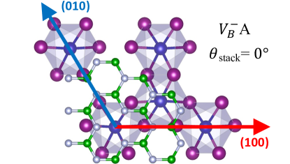
While the sign and magnitude of this effective exchange field can be postulated to vary, contingent on the stacking configuration between the hBN layer and CrI3 substrate, our first-principles calculations suggest that the interaction always favors AFM coupling across all stacking configurations, regardless of interlayer twist angle and lateral shift. To demonstrate this, we adopt a hBN flake structure hosting a defect at the center with hydrogen termination on the edge to model the quantum sensor. The flake structure (in comparison to extended structure) allows us to fully investigate the rotational and translational degree of freedom of the stacking dependence, free from the geometry constraint of supercells.
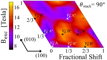
We start by considering a monolayer hBN with in direct contact with CrI3 (shown in Fig. 3a). As expected from our previous discussions, defect remains structurally and electronically stable upon stacked on CrI3. Due to the symmetry of , the heterostructure’s full interlayer twisting degree of freedom can be reduced to the range of , where is the relative in-plane rotation angles between hBN and CrI3. In total, 4 unique twist angles , each with a grid for lateral translation in the unit cell of CrI3, were sampled. The pattern of effective exchange field at and are shown in Fig. 3b and Fig. 3c, respectively. (see Supporting Information for data of ).
In order to verify that the findings obtained with the hBN flake method are not influenced by finite size effects, we also performed similar calculations using a periodic heterostructure comprised of hBN and CrI3. A grid within the unit cell of CrI3 is sampled and the heatmap of its effective exchange field is shown in Fig. 3d. The magnitude and direction of calculated using periodic heterostructure at is close to those obtained from the hBN flake method at .

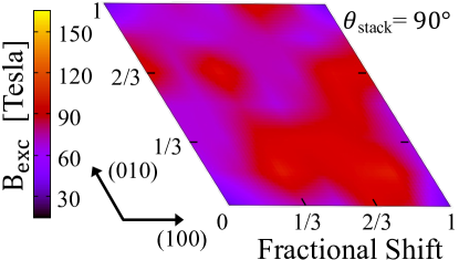
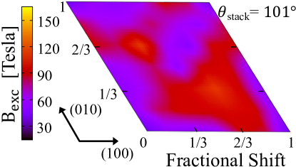
The average of effective exchange field over the sampled stacking configurations is T (equivalently meV), several orders of magnitude greater than typical size of magnetic dipole interaction. This value varies with a standard deviation of T, ranging between a minimum of T and a maximum of T. Interestingly, the direction of the exchange field, or the sign of from the calculations, stays unchanged throughout all stacking configurations. This contrasts with the spatially varying direction of stray fields generated by a 2D magnet at several angstroms away from the sample surface, as we will discuss later. Typically, quantum sensing protocol conducted with solid-state spin centers, such as the center in diamond, is performed by measuring the projected stray field to the spin center’s quantization axis. Spatial variation in direction can cause the projection, and hence the interaction magnitude, to fluctuate around zero, effectively hindering sensing at atomic level resolution. Relying on a fundamentally different mechanism, our proposed protocol showcases unidirectional AFM exchange field that promises high sensitivity in probing the magnetism.
I.4 Exchange Pathway
Next we discuss the dependence of the magnitude of on stacking order. We selectively highlighted two equivalent stacking orders, A’ and B’, in Fig. 3b. These particular stacking configurations were chosen for illustration because they respectively exhibits comparable magnitudes of in all the we calculated, suggesting a strong correlation between stacking order and .
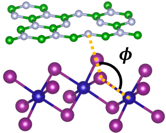
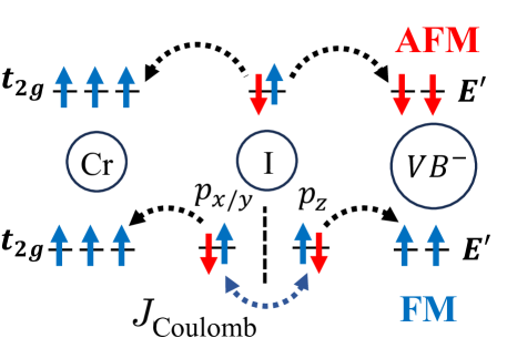
The microscopic mechanism of the interlayer coupling is an AFM superexchange between the Cr atoms in CrI3 and defect mediated by the I p-orbitals. The Cr atom in CrI3 is in a electronic configuration with 3 unpaired electrons in the orbitals at the valence top. The defect’s magnetic moment originates from 2 half filled orbitals [49]. Many exchange pathways between the defect and Cr are possible. We select six main superexchange pathways, which include nearest-neighbor I atoms in coordination with N atoms surrounding the defect and two adjacent Cr atoms, with an angle in each pathway, one of such pathway is illustrated in Fig. 4a. Fig. 4b demonstrates competing exchange interaction process between Cr atom and defect. When the angle of the exchange pathway approaches , both Cr orbitals and the orbitals couple to the same I p-orbital, which leads to an AFM superexchange. Conversely, as nears , the Cr orbitals and orbitals tend to couple to orthogonal I p-orbitals, favoring an interlayer FM superexchange via Coulomb exchange interactions on the I atom. This competition between interlayer AFM and FM superexchange is known as the Goodenough-Kanamori rule [50, 51, 52]. We then calculated the mean value of under different stacking configurations and found and are positively correlated, with a notable coefficient of determination of (see Supporting Information for detail). This strong correlation substantiates our theoretical analysis on the nature of interlayer superexchange interaction, which favors stronger AFM coupling as increases. We do no find including Hubbard U term to have pronounced influence on the property of this proximity-induced superexchange mechanism (see Supporting Information for more detail).
I.5 Sensing Across Multilayer hBN
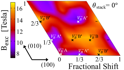
Given the significant exchange field when the center is situated in the first hBN layer above the magnetic substrate, we investigate a realistic scenario in which the defect spin center is separated by pristine BN layers from the sensing targets. This scenario mimics experiments where multiple layers BN are often stacked atop vdW magnets. We sample stacking configurations for a bilayer hBN (in its natural AA’ stacking) flake on the CrI3 heterostructure similar to the case of monolayer hBN/CrI3, but with an additional pristine hBN layer between the defect layer and the CrI3 substrate.
Despite the much larger spatial separation between the and CrI3, we discover large exchange field that always favors AFM coupling in the bilayer hBN/CrI3 system. The field averages to T (equivalently meV), with T and ranging between T and T. This is a surprising finding because the exchange pathway involves an additional pristine layer of hBN with large band gap, which introduces a barrier for the virtual hopping across the vdW gap. Fig. 5 shows the magnitude of when the defect is stacked onto CrI3 at different position. (see Supporting Information for full data) The exchange field maintains a similar magnitude across varied interlayer rotations and translations, exhibiting patterns consistent with those we discovered from first layer.
To understand the exchange interactions, we notice that with an extra pristine hBN layer, interlayer Cr- exchange is mediated by the I p-orbital and the pristine hBN’s p-orbital, therefore super-super-exchange in nature. Given the natural stacking configuration of the hBN layers, the vertical interlayer hopping between the orbitals of the defect and those in the pristine BN layers remains unchanged despite shifts and rotations of the bilayer relative to the CrI3 substrate. It is the hybridization between the pristine hBN and the CrI3 that determines the variation of orbital-dependent FM and AFM exchange competition. In comparison to the superexchange process, the super-super-exchange pathway now involves a B atom directly beneath a N atom adjacent to the , extending to an I atom, and finally connecting to the nearest neighbor Cr atom. Our first-principle results suggest that the characteristic AFM coupling, facilitated by the higher-order super-exchange through the layered hBN matrix, should be preserved even as the thickness of pristine hBN between the defect layer and CrI3 substrate increases, since it only contributes additional vertical B-N hoppings with no stacking dependence. Therefore, our proposed quantum sensing protocol driven by such exchange interaction can be extrapolated to structures incorporating more than one layer of pristine hBN, although systematic first-principles studies are unfeasible at this moment due to the higher computational cost.
I.6 Comparison to Stray Field Sensing
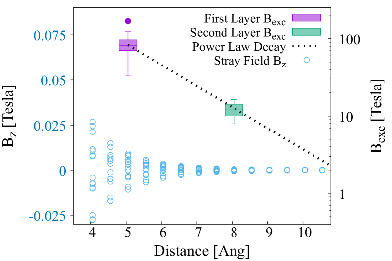
Furthermore, we analyze the dominance of exchange interaction over dipole-dipole interaction between the spin center and the magnetic substrate as the proximity changes. Fig. 6 represents the exchange interaction of various stacking configurations within the first two hBN layers and compares it with the component of stray field generated by CrI3 substrate that is periodic in the basal plane,
| (3) |
where is the vacuum permeability and is the magnetic moment of Cr atom. The stray field, arising from each Cr ion’s out-of-plane magnetic moment, is three orders of magnitude weaker than at close proximity. Moreover, while remains robustly AFM, exhibits spatial variations in sign, evident from its fluctuations around zero in Fig. 6.
The robust magnetic proximity effect in the presence of additional hBN layers suggests that the exchange interaction can dominate over dipole field even at larger distance. As the exchange interaction depends on the overlap of electronic wavefunction or hopping process, its magnitude should exhibit a power law decay as the distance or pathways become longer. Based on the decay rate from first to second layer of hBN, we anticipate that will reach the order of 0.1 mT at the seventh layer, thereby still maintaining its dominance over the stray field for spin center embedded in 3D structure.
II Summary
In this study, we introduces a novel quantum sensing scheme driven by the exchange interaction induced by the proximity between the spin center and magnetic sensing target. The practical implementation of this principle was explored utilizing the spin center in hBN proximate to a CrI3 magnetic substrate, employing ab-initio methods. Our calculation revealed a unidirectional and robust AFM exchange interaction between and CrI3. The exchange field is estimated to dominate over the magnetic dipole field with up to seven layers of pristine hBN between the spin center and the magnet.
As controlled generation of defect at different depths and positions has been experimentally demonstrated [32, 53], our proposed proximity-induced exchange interaction driven quantum sensing protocol can be readily realized using hBN coated cantilever or in fabricated heterostructure device. The principles established from the and CrI3 case may be applied to other optically active spin defects in 2D materials, such as WS2 [54]. On the other hand, the defect may also be applied to investigate magnetic materials with zero net magnetization, such as AFM materials. This is because the exchange interaction is primarily dominated by the direct or indirect overlap of electronic wavefunctions between quantum sensors and sensing targets, and the defect strongly couples to magnetic ions or layers in its immediate proximity, rather than the total dipole field. This study thereby pioneers a ultrasensitive in situ quantum sensing model driven by proximity-induced exchange interaction between quantum sensor and target, which may overcome intrinsic limitations of stray field sensing.
III Methods
All ab-initio calculations (except those specifically noted) were performed by using Density Functional Theory (DFT), with the Perdew-Burke-Ernzerhof (PBE) [55] functional for electron exchange and correlation potentials, as implemented in the VASP code [56]. We employed the projector augmented wave (PAW) [57] method for electron-ion interaction and an energy cutoff of 520 eV for wavefunction. Atomic coordinates are relaxed until forces on atom are smaller than eV/Å and the total energy was converged to be within eV. Van der Waal interactions is included as the DFT-D2 method [58]. Moreover, a Å vacuum layer is adopted to avoid interactions between repeating images.
For band alignment calculation, a hBN supercell containing one boron vacancy was used, with hBN lattice constant Å and centered k-point sampling. Monolayer unit cell of CrI3 and CrCl3 was used with lattice constant Å and Å respectively, with a centered k-point sampling for both. We use monolayer unit cell of CrSBr with lattice constant Å and Å with centered k-point sampling.
For the effective exchange field calculation, we use a circular flake structure with 41 B and 42 N atoms, containing one boron vacancy in the center and hydrogen termination on the edge. The underlying substrate contains a CrI3 unit cell in each periodic unit. We performed only k-point calculation. The alternative periodic supercell of hBN and CrI3 heterostructure is formed by a layer of 16 hBN unit cell on 4 CrI3 unit cell with centered k-point sampling.
IV Supporting Information
HSE06 band alignment, formation energy heatmap, correlation between exchange pathway angle and effective exchange field , influence of correlation effect on exchange interaction, POSCAR for VASP input, and raw data for effective exchange field.
V Acknowledgments
We thank Zeeshawn Kazi, Christian Pederson, Vasileios Niaouris, and Kai-Mei Fu for insightful discussions. The theoretical framework of quantum sensing at proximity is supported by the U.S. Department of Energy, Office of Science, National Quantum Information Science Research Centers, Co-design Center for Quantum Advantage (C2QA) under contract number DE-SC0012704. The first-principles investigation of magnetism and exchange coupling is based upon work supported by the National Science Foundation under Award No. DMR-2339995. This work was facilitated through the use of advanced computational, storage, and networking infrastructure provided by the Hyak supercomputer system and funded by the University of Washington Molecular Engineering Materials Center at the University of Washington. (NSF MRSEC DMR-2308979). This material is based in part upon work supported by the state of Washington through the University of Washington Clean Energy Institute.
References
- Degen et al. [2017] Degen, C.; Reinhard, F.; Cappellaro, P. Quantum sensing. Reviews of Modern Physics 2017, 89, 035002.
- Schirhagl et al. [2014] Schirhagl, R.; Chang, K.; Loretz, M.; Degen, C. L. Nitrogen-Vacancy Centers in Diamond: Nanoscale Sensors for Physics and Biology. Annual Review of Physical Chemistry 2014, 65, 83–105.
- Casola et al. [2018] Casola, F.; Van Der Sar, T.; Yacoby, A. Probing condensed matter physics with magnetometry based on nitrogen-vacancy centres in diamond. Nature Reviews Materials 2018, 3, 17088.
- Wolfowicz et al. [2021] Wolfowicz, G.; Heremans, F. J.; Anderson, C. P.; Kanai, S.; Seo, H.; Gali, A.; Galli, G.; Awschalom, D. D. Quantum guidelines for solid-state spin defects. Nature Reviews Materials 2021, 6, 906–925.
- Song et al. [2021] Song, T.; Sun, Q.-C.; Anderson, E.; Wang, C.; Qian, J.; Taniguchi, T.; Watanabe, K.; McGuire, M. A.; Stöhr, R.; Xiao, D.; Cao, T.; Wrachtrup, J.; Xu, X. Direct visualization of magnetic domains and moiré magnetism in twisted 2D magnets. Science 2021, 374, 1140–1144.
- Finco et al. [2021] Finco, A. et al. Imaging non-collinear antiferromagnetic textures via single spin relaxometry. Nature Communications 2021, 12, 767.
- Huang et al. [2023] Huang, M. et al. Revealing intrinsic domains and fluctuations of moiré magnetism by a wide-field quantum microscope. Nature Communications 2023, 14, 5259.
- Barry et al. [2016] Barry, J. F.; Turner, M. J.; Schloss, J. M.; Glenn, D. R.; Song, Y.; Lukin, M. D.; Park, H.; Walsworth, R. L. Optical magnetic detection of single-neuron action potentials using quantum defects in diamond. Proceedings of the National Academy of Sciences 2016, 113, 14133–14138.
- Aslam et al. [2023] Aslam, N.; Zhou, H.; Urbach, E. K.; Turner, M. J.; Walsworth, R. L.; Lukin, M. D.; Park, H. Quantum sensors for biomedical applications. Nature Reviews Physics 2023, 5, 157–169.
- Koehl et al. [2011] Koehl, W. F.; Buckley, B. B.; Heremans, F. J.; Calusine, G.; Awschalom, D. D. Room temperature coherent control of defect spin qubits in silicon carbide. Nature 2011, 479, 84–87.
- Zhang et al. [2020] Zhang, G.; Cheng, Y.; Chou, J.-P.; Gali, A. Material platforms for defect qubits and single-photon emitters. Applied Physics Reviews 2020, 7, 031308.
- Freysoldt et al. [2014] Freysoldt, C.; Grabowski, B.; Hickel, T.; Neugebauer, J.; Kresse, G.; Janotti, A.; Van De Walle, C. G. First-principles calculations for point defects in solids. Reviews of Modern Physics 2014, 86, 253–305.
- Maze et al. [2008] Maze, J. R.; Stanwix, P. L.; Hodges, J. S.; Hong, S.; Taylor, J. M.; Cappellaro, P.; Jiang, L.; Dutt, M. V. G.; Togan, E.; Zibrov, A. S.; Yacoby, A.; Walsworth, R. L.; Lukin, M. D. Nanoscale magnetic sensing with an individual electronic spin in diamond. Nature 2008, 455, 644–647.
- Kolkowitz et al. [2015] Kolkowitz, S.; Safira, A.; High, A. A.; Devlin, R. C.; Choi, S.; Unterreithmeier, Q. P.; Patterson, D.; Zibrov, A. S.; Manucharyan, V. E.; Park, H.; Lukin, M. D. Probing Johnson noise and ballistic transport in normal metals with a single-spin qubit. Science 2015, 347, 1129–1132.
- Steinert et al. [2013] Steinert, S.; Ziem, F.; Hall, L. T.; Zappe, A.; Schweikert, M.; Götz, N.; Aird, A.; Balasubramanian, G.; Hollenberg, L.; Wrachtrup, J. Magnetic spin imaging under ambient conditions with sub-cellular resolution. Nature Communications 2013, 4, 1607.
- Romach et al. [2015] Romach, Y.; Müller, C.; Unden, T.; Rogers, L.; Isoda, T.; Itoh, K.; Markham, M.; Stacey, A.; Meijer, J.; Pezzagna, S.; Naydenov, B.; McGuinness, L.; Bar-Gill, N.; Jelezko, F. Spectroscopy of Surface-Induced Noise Using Shallow Spins in Diamond. Physical Review Letters 2015, 114, 017601.
- Bluvstein et al. [2019] Bluvstein, D.; Zhang, Z.; Jayich, A. C. B. Identifying and Mitigating Charge Instabilities in Shallow Diamond Nitrogen-Vacancy Centers. Physical Review Letters 2019, 122, 076101.
- Attaccalite et al. [2013] Attaccalite, C.; Wirtz, L.; Marini, A.; Rubio, A. Efficient Gate-tunable light-emitting device made of defective boron nitride nanotubes: from ultraviolet to the visible. Scientific Reports 2013, 3, 2698.
- Durand et al. [2023] Durand, A.; Clua-Provost, T.; Fabre, F.; Kumar, P.; Li, J.; Edgar, J.; Udvarhelyi, P.; Gali, A.; Marie, X.; Robert, C.; Gérard, J.; Gil, B.; Cassabois, G.; Jacques, V. Optically Active Spin Defects in Few-Layer Thick Hexagonal Boron Nitride. Physical Review Letters 2023, 131, 116902.
- Gottscholl et al. [2021] Gottscholl, A.; Diez, M.; Soltamov, V.; Kasper, C.; Sperlich, A.; Kianinia, M.; Bradac, C.; Aharonovich, I.; Dyakonov, V. Room temperature coherent control of spin defects in hexagonal boron nitride. Science Advances 2021, 7, eabf3630.
- Gottscholl et al. [2020] Gottscholl, A.; Kianinia, M.; Soltamov, V.; Orlinskii, S.; Mamin, G.; Bradac, C.; Kasper, C.; Krambrock, K.; Sperlich, A.; Toth, M.; Aharonovich, I.; Dyakonov, V. Initialization and read-out of intrinsic spin defects in a van der Waals crystal at room temperature. Nature Materials 2020, 19, 540–545.
- Chen and Quek [2021] Chen, Y.; Quek, S. Y. Photophysical Characteristics of Boron Vacancy-Derived Defect Centers in Hexagonal Boron Nitride. The Journal of Physical Chemistry C 2021, 125, 21791–21802.
- Mathur et al. [2022] Mathur, N.; Mukherjee, A.; Gao, X.; Luo, J.; McCullian, B. A.; Li, T.; Vamivakas, A. N.; Fuchs, G. D. Excited-state spin-resonance spectroscopy of defect centers in hexagonal boron nitride. Nature Communications 2022, 13, 3233.
- Healey et al. [2023] Healey, A. J.; Scholten, S. C.; Yang, T.; Scott, J. A.; Abrahams, G. J.; Robertson, I. O.; Hou, X. F.; Guo, Y. F.; Rahman, S.; Lu, Y.; Kianinia, M.; Aharonovich, I.; Tetienne, J.-P. Quantum microscopy with van der Waals heterostructures. Nature Physics 2023, 19, 87–91.
- Huang et al. [2022] Huang, M.; Zhou, J.; Chen, D.; Lu, H.; McLaughlin, N. J.; Li, S.; Alghamdi, M.; Djugba, D.; Shi, J.; Wang, H.; Du, C. R. Wide field imaging of van der Waals ferromagnet Fe3GeTe2 by spin defects in hexagonal boron nitride. Nature Communications 2022, 13, 5369.
- Gottscholl et al. [2021] Gottscholl, A.; Diez, M.; Soltamov, V.; Kasper, C.; Krauße, D.; Sperlich, A.; Kianinia, M.; Bradac, C.; Aharonovich, I.; Dyakonov, V. Spin defects in hBN as promising temperature, pressure and magnetic field quantum sensors. Nature Communications 2021, 12, 4480.
- Dean et al. [2010] Dean, C. R.; Young, A. F.; Meric, I.; Lee, C.; Wang, L.; Sorgenfrei, S.; Watanabe, K.; Taniguchi, T.; Kim, P.; Shepard, K. L.; Hone, J. Boron nitride substrates for high-quality graphene electronics. Nature Nanotechnology 2010, 5, 722–726.
- Radisavljevic et al. [2011] Radisavljevic, B.; Radenovic, A.; Brivio, J.; Giacometti, V.; Kis, A. Single-layer MoS2 transistors. Nature Nanotechnology 2011, 6, 147–150.
- Novoselov et al. [2016] Novoselov, K. S.; Mishchenko, A.; Carvalho, A.; Castro Neto, A. H. 2D materials and van der Waals heterostructures. Science 2016, 353, aac9439.
- Stern et al. [2022] Stern, H. L.; Gu, Q.; Jarman, J.; Eizagirre Barker, S.; Mendelson, N.; Chugh, D.; Schott, S.; Tan, H. H.; Sirringhaus, H.; Aharonovich, I.; Atatüre, M. Room-temperature optically detected magnetic resonance of single defects in hexagonal boron nitride. Nature Communications 2022, 13, 618.
- Li and Gali [2022] Li, S.; Gali, A. Identification of an Oxygen Defect in Hexagonal Boron Nitride. The Journal of Physical Chemistry Letters 2022, 13, 9544–9551.
- Guo et al. [2022] Guo, N.-J. et al. Generation of Spin Defects by Ion Implantation in Hexagonal Boron Nitride. ACS Omega 2022, 7, 1733–1739.
- Jin et al. [2009] Jin, C.; Lin, F.; Suenaga, K.; Iijima, S. Fabrication of a Freestanding Boron Nitride Single Layer and Its Defect Assignments. Physical Review Letters 2009, 102, 195505.
- Mendelson et al. [2021] Mendelson, N. et al. Identifying carbon as the source of visible single-photon emission from hexagonal boron nitride. Nature Materials 2021, 20, 321–328.
- Chejanovsky et al. [2021] Chejanovsky, N.; Mukherjee, A.; Geng, J.; Chen, Y.-C.; Kim, Y.; Denisenko, A.; Finkler, A.; Taniguchi, T.; Watanabe, K.; Dasari, D. B. R.; Auburger, P.; Gali, A.; Smet, J. H.; Wrachtrup, J. Single-spin resonance in a van der Waals embedded paramagnetic defect. Nature Materials 2021, 20, 1079–1084.
- Liu et al. [2022] Liu, W. et al. Coherent dynamics of multi-spin center in hexagonal boron nitride. Nature Communications 2022, 13, 5713.
- Gao et al. [2022] Gao, X.; Vaidya, S.; Li, K.; Ju, P.; Jiang, B.; Xu, Z.; Allcca, A. E. L.; Shen, K.; Taniguchi, T.; Watanabe, K.; Bhave, S. A.; Chen, Y. P.; Ping, Y.; Li, T. Nuclear spin polarization and control in hexagonal boron nitride. Nature Materials 2022, 21, 1024–1028.
- Liu et al. [2021] Liu, W. et al. Temperature-Dependent Energy-Level Shifts of Spin Defects in Hexagonal Boron Nitride. ACS Photonics 2021, 8, 1889–1895.
- Lyu et al. [2022] Lyu, X.; Tan, Q.; Wu, L.; Zhang, C.; Zhang, Z.; Mu, Z.; Zúñiga-Pérez, J.; Cai, H.; Gao, W. Strain Quantum Sensing with Spin Defects in Hexagonal Boron Nitride. Nano Letters 2022, 22, 6553–6559.
- Yang et al. [2022] Yang, T.; Mendelson, N.; Li, C.; Gottscholl, A.; Scott, J.; Kianinia, M.; Dyakonov, V.; Toth, M.; Aharonovich, I. Spin defects in hexagonal boron nitride for strain sensing on nanopillar arrays. Nanoscale 2022, 14, 5239–5244.
- Lu et al. [2020] Lu, X.; Fei, R.; Zhu, L.; Yang, L. Meron-like topological spin defects in monolayer CrCl3. Nature Communications 2020, 11, 4724.
- Huang et al. [2017] Huang, B.; Clark, G.; Navarro-Moratalla, E.; Klein, D. R.; Cheng, R.; Seyler, K. L.; Zhong, D.; Schmidgall, E.; McGuire, M. A.; Cobden, D. H.; Yao, W.; Xiao, D.; Jarillo-Herrero, P.; Xu, X. Layer-dependent ferromagnetism in a van der Waals crystal down to the monolayer limit. Nature 2017, 546, 270–273.
- Cai et al. [2019] Cai, X.; Song, T.; Wilson, N. P.; Clark, G.; He, M.; Zhang, X.; Taniguchi, T.; Watanabe, K.; Yao, W.; Xiao, D.; McGuire, M. A.; Cobden, D. H.; Xu, X. Atomically Thin CrCl : An In-Plane Layered Antiferromagnetic Insulator. Nano Letters 2019, 19, 3993–3998.
- Lee et al. [2021] Lee, K.; Dismukes, A. H.; Telford, E. J.; Wiscons, R. A.; Wang, J.; Xu, X.; Nuckolls, C.; Dean, C. R.; Roy, X.; Zhu, X. Magnetic Order and Symmetry in the 2D Semiconductor CrSBr. Nano Letters 2021, 21, 3511–3517.
- Telford et al. [2020] Telford, E. J.; Dismukes, A. H.; Lee, K.; Cheng, M.; Wieteska, A.; Bartholomew, A. K.; Chen, Y.; Xu, X.; Pasupathy, A. N.; Zhu, X.; Dean, C. R.; Roy, X. Layered Antiferromagnetism Induces Large Negative Magnetoresistance in the van der Waals Semiconductor CrSBr. Advanced Materials 2020, 32, 2003240.
- Heyd et al. [2003] Heyd, J.; Scuseria, G. E.; Ernzerhof, M. Hybrid functionals based on a screened Coulomb potential. The Journal of Chemical Physics 2003, 118, 8207–8215.
- Krukau et al. [2006] Krukau, A. V.; Vydrov, O. A.; Izmaylov, A. F.; Scuseria, G. E. Influence of the exchange screening parameter on the performance of screened hybrid functionals. The Journal of Chemical Physics 2006, 125, 224106.
- Xu et al. [2018] Xu, C.; Feng, J.; Xiang, H.; Bellaiche, L. Interplay between Kitaev interaction and single ion anisotropy in ferromagnetic CrI3 and CrGeTe3 monolayers. npj Computational Materials 2018, 4, 1–6.
- Abdi et al. [2018] Abdi, M.; Chou, J.-P.; Gali, A.; Plenio, M. B. Color Centers in Hexagonal Boron Nitride Monolayers: A Group Theory and Ab Initio Analysis. ACS Photonics 2018, 5, 1967–1976.
- Goodenough [1955] Goodenough, J. B. Theory of the Role of Covalence in the Perovskite-Type Manganites . Physical Review 1955, 100, 564–573.
- Goodenough [1958] Goodenough, J. B. An interpretation of the magnetic properties of the perovskite-type mixed crystals La1-xSrxCoO3-λ. Journal of Physics and Chemistry of Solids 1958, 6, 287–297.
- Kanamori [1959] Kanamori, J. Superexchange interaction and symmetry properties of electron orbitals. Journal of Physics and Chemistry of Solids 1959, 10, 87–98.
- Gao et al. [2021] Gao, X.; Jiang, B.; Llacsahuanga Allcca, A. E.; Shen, K.; Sadi, M. A.; Solanki, A. B.; Ju, P.; Xu, Z.; Upadhyaya, P.; Chen, Y. P.; Bhave, S. A.; Li, T. High-Contrast Plasmonic-Enhanced Shallow Spin Defects in Hexagonal Boron Nitride for Quantum Sensing. Nano Letters 2021, 21, 7708–7714.
- Li et al. [2022] Li, S.; Thiering, G.; Udvarhelyi, P.; Ivády, V.; Gali, A. Carbon defect qubit in two-dimensional WS2. Nature Communications 2022, 13, 1210.
- Perdew et al. [1996] Perdew, J. P.; Burke, K.; Ernzerhof, M. Generalized Gradient Approximation Made Simple. Physical Review Letters 1996, 77, 3865–3868.
- Kresse and Furthmüller [1996] Kresse, G.; Furthmüller, J. Efficiency of ab-initio total energy calculations for metals and semiconductors using a plane-wave basis set. Computational Materials Science 1996, 6, 15–50.
- Kresse and Joubert [1999] Kresse, G.; Joubert, D. From ultrasoft pseudopotentials to the projector augmented-wave method. Physical Review B 1999, 59, 1758–1775.
- Grimme [2006] Grimme, S. Semiempirical GGA-type density functional constructed with a long-range dispersion correction. Journal of Computational Chemistry 2006, 27, 1787–1799.