-
April 2024
Spin-NeuroMem: A Low-Power Neuromorphic Associative Memory Design Based on Spintronic Devices
Abstract
Biologically-inspired computing models have made significant progress in recent years, but the conventional von Neumann architecture is inefficient for the large-scale matrix operations and massive parallelism required by these models. This paper presents Spin-NeuroMem, a low-power circuit design of Hopfield network for the function of associative memory. Spin-NeuroMem is equipped with energy-efficient spintronic synapses which utilize magnetic tunnel junctions (MTJs) to store weight matrices of multiple associative memories. The proposed synapse design achieves as low as 17.4% power consumption compared to the state-of-the-art synapse designs. Spin-NeuroMem also encompasses a novel voltage converter with 60% less transistor usage for effective Hopfield network computation. In addition, we propose an associative memory simulator for the first time, which achieves a 5.05M speedup with a comparable associative memory effect. By harnessing the potential of spintronic devices, this work sheds light on the development of energy-efficient and scalable neuromorphic computing systems. The source code will be publicly available after the manuscript is reviewed.
Keywords: Neuromorphic computing, Associative memory, Spintronic devices, Low-power.
1 Introduction
Neuromorphic computing (NC) [1, 2] mimics brain functionalities through complex connections between a large number of artificial neurons and synapses, resulting in powerful computing capabilities. Owning to its great potential for applying to energy-efficient pattern recognition, associative memory, and decision-making beyond the traditional von Neumann architecture, NC has become a strong candidate to evolve into a new computing paradigm in the future. The goal of NC research is to emulate neurons and synapses of the human brain by capturing the behaviors of emerging devices at nanoscale, overcoming the limitations of traditional computing modes. As a typical feedback-based NC model, Hopfield network maps input patterns to stable output states to achieve various functionalities including associative memory, error correction, categorization, familiarity recognition, and time sequence retention [3]. Among these functionalities, associative memory is the most promising application of Hopfield networks, attracting great research attention[4] due to its ability to restore the complete picture of a given data set from partial information, similar to human memory.
Efficient execution of NC relies on the prerequisite of hardware implementation. Conventionally, hardware implementations of the Hopfield network are typically based on complementary metal-oxide-semiconductor (CMOS) technology, which faces challenges related to area and power consumption. In recent years, the emergence of new devices such as memristors [5] offers an opportunity. However, NC systems demand repeated current stimulation to memristive synapses, leading to device resistance drift. This inevitably instigates weight variations that damage the reliability of synapse [6, 7]. Additionally, many challenges on endurance and defect rates need to be addressed when using memristors. Unlike memristors, spintronic devices such as magnetic tunnel junctions (MTJs) provide new possibilities for reliable synaptic design thanks to the fact that they exploit electron spin rather than electron charge for memory read and write [8, 9, 10]. However, designing advanced spintronic-based NC systems still faces many challenges, including: 1) the production of special MTJs remains difficult [8]; 2) insufficient device reliability under process variations (PVs) [9]; 3) dramatic increase in power consumption as the number of synaptic weights increases [10]. Therefore, it is imperative to design a reliabile neural computing system with scalable synaptic weights, while achieving low power consumption and high PV tolerance.
In this paper, we presents a low-power neuromorphic associative memory design named Spin-NeuroMem. It utilizes spintronic devices to design synapses for storing weight matrices for multiple associative memories. The proposed synapse design significantly reduces power consumption compared to existing solutions. The non-volatile property of MTJs allows our circuit to be completely powered off during inactive phases, which further reduces the leakage power of our design.
Our contributions in this paper can be summarized as follows:
-
•
We present a novel voltage converter for hardware-based Hopfield networks. Our design utilizes a modified logic gate circuit to obtain binary-to-Hopfield-network conversion, resulting in a 60% reduction in transistor count compared to the existing work.
-
•
We propose a spintronic synapse composed of MTJ matrices that can provide different weights to support neural computation. Our design is remarkably energy-efficient, with a power consumption of only 17.4% of the previous work for ten positive-weight synapses.
-
•
We develop an associative memory simulator to evaluate the performance of our Spin-NeuroMem at large scale. By evaluating the simulated Spin-NeuroMem, we assessed its nearly equivalent associative memory effect to the software-based Hopfied network with a 5.05M speedup.
The structure of this paper is organized as follows. In Section 2, we review the basic principle of associative memory and the fundamental concepts of MTJ technology. Section 3 provides detailed explanations of the design principles and circuit implementation of Spin-NeuroMem. In Section 4, we evaluate and analyze the associative memory functionality of Spin-NeuroMem at the circuit and system levels. Finally, Section 5 concludes the entire paper.
2 Background
2.1 Hopfield Network and Associative Memory
The Hopfield neural network [3] is generally used to solve combinatorial optimization problems or implement associative memory for pattern recognition. Associative memory is similar to the human brain memory that can recall the memorized data by providing a portion of the data or noisy data rather than by giving an address in the existing semiconductor memories [4].
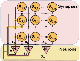
The Hopfield network is a single-layer, fully connected recurrent neural network composed of neurons and synapses, as shown in Fig. 1. The working principle of the Hopfield network model can be expressed by:
| (1) | ||||
| (2) | ||||
| (3) |
In the above equations, represents the weight of synaptic connecting the -th and -th neurons and , represents the output of the -th neuron at time . represents the state of the -th neuron at time ; it is calculated by summing up every row of the product along column at time . The output of neuron at is determined by the function and . represents the threshold of the -th neuron. For instance, as the highlighted path in Fig. 1 illustrates, when the presynaptic neuron outputs at time , it is transmitted through the synaptic to the postsynaptic neuron . The electrical potential , which accumulates all the incoming signals to , determines whether or not is activated, thus concluding a round of neural signal transmission.
To memorize patterns, each of which is denoted as a vector , the learned result of the weight matrix can be derived as:
| (4) |
Note that each element of the matrix .
2.2 Magnetic Tunnel Junction
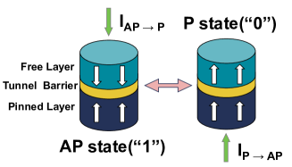
MTJs are widely-used spintronic devices that have a three-layer structure [11, 12, 13, 14]. As shown in Fig. 2, this structure consists of two ferromagnetic layers separated by a dielectric tunnel barrier (TB) layer. The lower ferromagnetic layer, known as the pinned layer (PL), has its magnetization fixed along the easy axis of the MTJ[15]. The upper ferromagnetic layer, named free layer (FL), can have its magnetization parallel (P) or antiparallel (AP) to that of the PL[16]. Due to the tunnelling magneto-resistance (TMR) effect[17], the resistance value () is higher in the AP state and referred to as logic “1”, while in the P state, the resistance value () is lower and referred to as logic “0”. The difference between these two resistance values is expressed by the TMR ratio:
| (5) |
The resistive state of MTJ can be switched by applying a spin-polarized current [18]. Fig. 2 shows that a positive pulse across the MTJ in the AP state drives a current perpendicularly from the FL to the PL. When certain thresholds for pulse amplitude and width are surpassed (typically -), the magnetization of the FL switches its direction. In a similar manner, a negative pulse exceeding the critical switching current under the spin-polarized current can switch the MTJ from P to AP. Due to the stable binary magnetic states (i.e., AP and P), and do not show a degradation trend as found in memristors over writing cycles. [19].
In summary, MTJs are perfect candidates for synaptic design, owning to non-volatility, re-programability, low-power. In addition, MTJs feature almost no resistance drift over time, which overcomes the limitations of hardware NC systems based on memristors.
2.3 Related Work
Next, we review the research advancement in NC implementation based on novel devices, including memristors and spintronic devices.
2.3.1 Memristor-based Neuromorphic Hardware
The work in [4] demonstrates an associative memory implementation using a memristive Hopfield network. It presents adjustable resistance in memristors for pattern storage and retrieval, as well as programmable synaptic weights in a 3-bit memristive Hopfield network. The design in [20] adopts a memristor-based annealing system with a neuromorphic architecture, providing a high-throughput solution for NP-hard problems through parallel operations and leveraging hardware noise for improved efficiency.
Despite some pioneering attempts, the application of memristors in NC is limited by its physical characteristics. For example, the resistive drift over time caused by electric field changes and atomic migration inevitably leads to variations in synaptic weights [21]. Additionally, many challenges on durability and defect rates need to be addressed when using memristors [22].
2.3.2 Spintronic-based Neuromorphic Hardware
Unlike memristors, spintronic devices such as MTJs provide new possibilities for reliable synaptic design thanks to the fact that they exploit electron spin rather than electron charge for memory read and write.
The compound spintronic synapse design in [8] shows promise for NC with its stable multiple resistance states, but challenges remain in addressing PVs and achieving consistent material and thickness of stacked MTJs. The spintronic synapse proposed in [9] demonstrates associative memory operations using an antiferromagnet/ferromagnet heterostructure driven by spin-orbit torque, but its stability against process, voltage, and temperature variations remains challenging due to device variability and non-linearity.
A novel nonvolatile associative memory based on spintronic synapses and carbon nanotube field-effect transistor (CNTFET) neurons is proposed in [10]. MTJs provide configurability, nonvolatility, and high endurance to the design, while CNTFETs compensate for the limitations of conventional transistors in deep nanoscale nodes. Although the design offers significant power advantages over its counterpart with CMOS devices, the synaptic design that utilizes serially-connected MTJs for multiple weights inevitably leads to increased power consumption. Moreover, the voltage adder which is required for each synapse occupies unnecessary on-chip area.
3 Proposed Spin-NeuroMem Design
In this section, we first provide an overview of the proposed Spin-NeuroMem design. Thereafter, we elaborate the structures and functionalities of each component in the design.
3.1 Design Overview
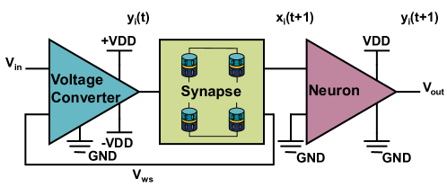
Fig. 3 shows constituent parts of Spin-NeuroMem, including voltage converters, synapses, and neurons. The voltage converter takes a binary value (0 or 1) as input from external or feedback from presynaptic neurons and outputs a bipolar value (-1 or 1) for synaptic activation. The synaptic activation generates an analog voltage that contains weight information, which is then transmitted to postsynaptic neurons. The postsynaptic neuron receives incoming signals from all connected presynaptic neurons through synapses, sums them up, and updates its output value through an activation function, which finally results in a binary value (0 and 1). This process corresponds to a neural activation from a presynaptic neuron to a postsynaptic neuron, as highlighted in Fig. 1.

3.2 Voltage Converter Design
| 0 | 0 | -1 |
| 0 | 1 | 1 |
| 1 | 0 | 1 |
| 1 | 1 | -1 |
The voltage converter design includes an XNOR gate and a modified inverter-like structure, as shown in Fig. 4. The XNOR gate takes inputs and , representing the input from the presynaptic neuron and the sign of the weight read from that synapse, respectively. The output of the voltage converter, , is the converted output voltage that is then provided to the synapse. Table 1 presents the logic values of , , and along with their conversion relationships.
The proposed voltage converter significantly saves on-chip area compared to the prior CNTFET-based voltage adder[10]. The evaluation of area employs the same methodology as that used in [23]On the technology node, the single voltage adder proposed in [10] exhibits an area of , whereas the area of our proposed voltage converter is . This means a 60% reduction in the area. In other words, implementing a Hopfield network capable of processing the MNIST dataset [24], composed of 784 neurons and 614656 synapses, could save an area of approximately.
3.3 Synapse Design
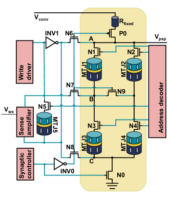
In the information transmission process, neurotransmitters are released by pre-synaptic neurons and can affect the action potential of post-synaptic neurons via the synapses. Our spintronic synapses have been designed to mimic this communication process, providing varying weights as depicted in Fig. 5. Each synapse comprises MTJs ( in this case), including MTJs for controlling the weight values and one MTJ for controlling the weight sign. This results in a total of positive weights and negative weights.
Our synapse design can work in two different modes, i.e., associative memory mode and configuration mode, depending on the signal from the synamptic controller. When the synaptic controller outputs “1”, the associative memory mode is activated. In this case, transistors N0 and P0 are turned on, while transistors N6, N7, N8, and N9 are turned off. Focusing on the black wire section of the circuit, we observe that each of the four MTJs has different resistance values in the AP and P states due to the TMR effect. Consequently, five weight configurations determine the synaptic strength: 4, 31, 22, 13, and 4. The input of the synapse is corresponds to the voltage converter output, and output is the postsynaptic potential voltage (), which will be transmitted to the postsynaptic neuron. Assuming , , and are the resistance values of the four MTJs in the MTJ matrix, and is the fixed resistance, and can be expressed as:
| (6) |
In order to achieve the maximum swing of , the value of should be approximately halfway between and . Note that some weight configurations, like 22, correspond to different MTJ matrix configurations (e.g., and or and configured as AP). However, we only program one of them as the effective weight to ensure large and uniform weight differences. MTJ5 in Fig. 5 memories the weight sign, which is read out by the sense amplifier and fed back to the voltage converter to control direction achieving fully non-volatile storage of the weight values.
When the synaptic controller outputs “0”, the configuration mode is activated. MTJs receive write current from bottom to top or top to bottom depending on the output of the write driver. The address decoder controls the gate of transistors N1, N2, N3, N4, and N5 that are connected in series with the MTJ. They are turned on to select the MTJ to be configured. More detailed description of the configuration process can be found in Section 4.2. It is worthing noting that the synapse configuration cost is not a concern as weight rewriting occurs only once during the process of weight learning.
Our 5-MTJ synapse design can be extended for more weight requirements as the total resistance range of spintronic synapses remains unchanged. A perpendicular MTJ based on the MgO/CoFeB structure has achieved a TMR of 249% [25]. Our design build on the current achievable advanced manufacturing process. Higher TMR ratio in MTJs of the future will allow for more weighting options in spintronic synapses.
3.4 Neuron Design
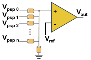
The neuron design originates from the CNTFET neuron proposed in [10]. In Fig. 6, the presynaptic neurons output postsynaptic potentials through synapses. After calculating , the resistive voltage adder within the neuron transmits the result to a single pin of a CMOS-based comparator. The other pin is the reference voltage , which is set to . Once the sum of the voltages exceeds the threshold, the neuron is activated and outputs “1”; otherwise, it remains inactive and outputs “0”.
4 Experiments and Evaluation
In this section, we first elaborate the experimental setups at both circuit and system levels. Thereafter, we present circuit simulation results of Spin-NeuroMem and evaluate its functionalities, performance, and power consumption. In addition, we perform system-level experiments and evaluation using an in-house Python simulator. To demonstrate the advantage of our proposed design, we also compare the performance of Spin-NeuroMem with that of the prior work as well as software implementations of associative memory.
| Parameter | Description | Value |
|---|---|---|
| Thickness of the free layer | ||
| Standard deviation of | 3% of | |
| Critical diameter | ||
| Thickness of the tunnel barrier | ||
| Standard deviation of | 3% of | |
| TMR ratio | 249% | |
| Standard deviation of TMR | 3% of 249% |
4.1 Experimental Setup
We conducted circuit simulations using Cadence Virtuoso tools with the MTJ compact model in [26] and Cadence generic process development kit (GPDK) technology. We took into account PV and estimated synapse weight drifts through Monte Carlo simulations. The critical parameters of the MTJ model and its PV strengths are provided in Table 2. The TMR value is consistent with the current capabilities of advanced manufacturing processes [25]. Note that PV is introduced by considering 3 deviation for the key device parameters. All circuit-level simulations were conducted under the ambient temperature of . Additionally, to facilitate a fair comparison, the previous work was re-experimented with identical parameters.
Due to the exponential overhead in time and computing resources to simulate a large-scale associate memory, circuit simulation is unsuitable to evaluate the performance of Spin-NeuroMem at system level. Consequently, we have developed a Python-based simulator, which will be open-sourced. To ensure simulation accuracy and consistency, circuit parameters were extracted from comprehensive circuit simulations and subsequently fed into the simulator. This ensures our simulator accurately replicates the circuit functionalities and performance exhibited during circuit-level simulations. The software-based Hopfield network were developed using Python 3.7 in both serial and parallel modes. The code were run on Ubuntu 20.04.1 with an Intel i9-12900 CPU. We compared the system-level performance using two metrics which are recall rate and recall latency. The recall rate is calculated by conducting retrieval experiments with noisy patterns input into Spin-NeuroMem. A successful recall occurs when the recalled pattern matches the original pattern. The recall rate is then determined through numerous retrieval attempts. The recall latency is the delay from pattern input to Spin-NeuroMem to output.
(a) Voltage converter
(b) Synapse
4.2 Circuit Simulation
4.2.1 Functional evaluation
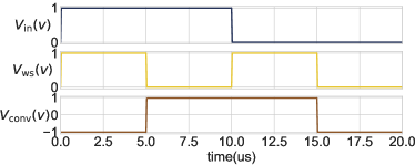
Fig. 7(a) depicts the functionality of the voltage converter via transient simulation. It can be seen that a of “1” results in a of “1” if the synaptic weight sign () is positive, otherwise it would be “-1”. Similarly, when is “0” and is positive, the resultant value is “-1”; otherwise, it would be “1”. The complete binary-to-bipolar conversion relations can be found in Table 1.
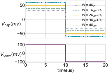
Fig. 7(b) shows the diverse weight selection capabilities of the all-spin neural synapse. Note that is transmitted from the previous stage. When it is “1”, five positive weight outputs are generated depending on different MTJ resistance configurations of the MTJ array. In a similar manner, five negative weight outputs are produced when is “-1”.
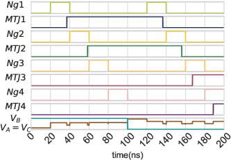
Fig. 8 presents the functional simulation of synaptic weight configuration process, when the synaptic controller output is set to “0” (configuration mode). In the figure, Ng1-Ng4 correspond to the gate signals of the NMOS transistors that select the four MTJ devices (N1-N4) shown in Fig. 5, while MTJ1-MTJ4 denote the magnetization state of the corresponding MTJ devices; , , and represent the voltage at points A, B, and C, respectively.
The write driver initially outputs a high signal for . If the NMOS transistor connected in series with the MTJ is turned on at this time, the MTJ array can receive write current from both A-B and C-B directions. In the initial state of the simulation, all four MTJs are in P-state, representing a logic “0”. The gate voltages of N1, N2, N3, and N4 increase sequentially by . MTJ1 and MTJ2 are written to “1”, while MTJ3 and MTJ4 are configured to “0”. Subsequently, the write driver outputs a low signal for . At this time, if the NMOS transistor connected in series with the MTJ is turned on, the write current flows through the MTJ array in the opposite direction. After a delay, the four MTJs are set to “0”, “0”, “1”, “1”, respectively.
4.2.2 Impact of device variations on weight
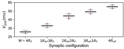
To evaluate the functionality of spin-based synapses in the presence of PV, we took into account a 3% variation in the parameters listed in Table 2 in the MTJ model and conducted Monte Carlo simulations. We conducted 1 000 simulations for each synaptic weight configuration, resulting in a total of 5 000 simulations considering only positive weights in synaptic connections based on a MTJ matrix neural synapse shown in Fig. 5. In Fig. 9, we observed that the upper and lower quartiles of output voltage, obtained through the synaptic weights, showed a significant difference for the MTJ matrix-based neural synapse.
4.2.3 Power consumption
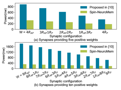
To compare the power consumption of our proposed design with previous work, we conducted a comparison between the power consumption of the synaptic connection presented in this paper and that in [10], under the same transistor and MTJ process parameters. Fig. 10(a) shows five neural synapses based on MTJ matrices, providing five positive weights. Our design significantly reduces power consumption, ranging from 36.1% to 32.2% of the previous work under the five synaptic weights, measured in . Furthermore, our design exhibits minimal increase in power consumption as the number of weights increases. Fig. 10(b) shows a comparison between the power consumption of synapses that use more MTJs to provide more weights. Increasing the scale of reconfigurable MTJs in the spintronic synapse results in a noticeable increase in power consumption in [10]. while our disign maintains the same power consumption range, ranging from 17.4% to 28.9% of the previous work, measured in .
4.3 Systematic Performance Evaluation
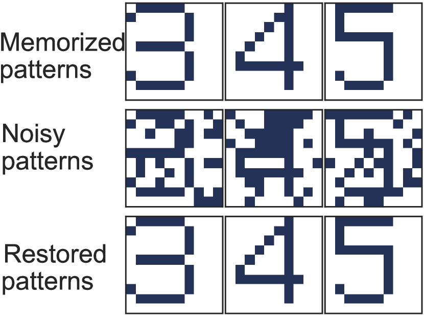
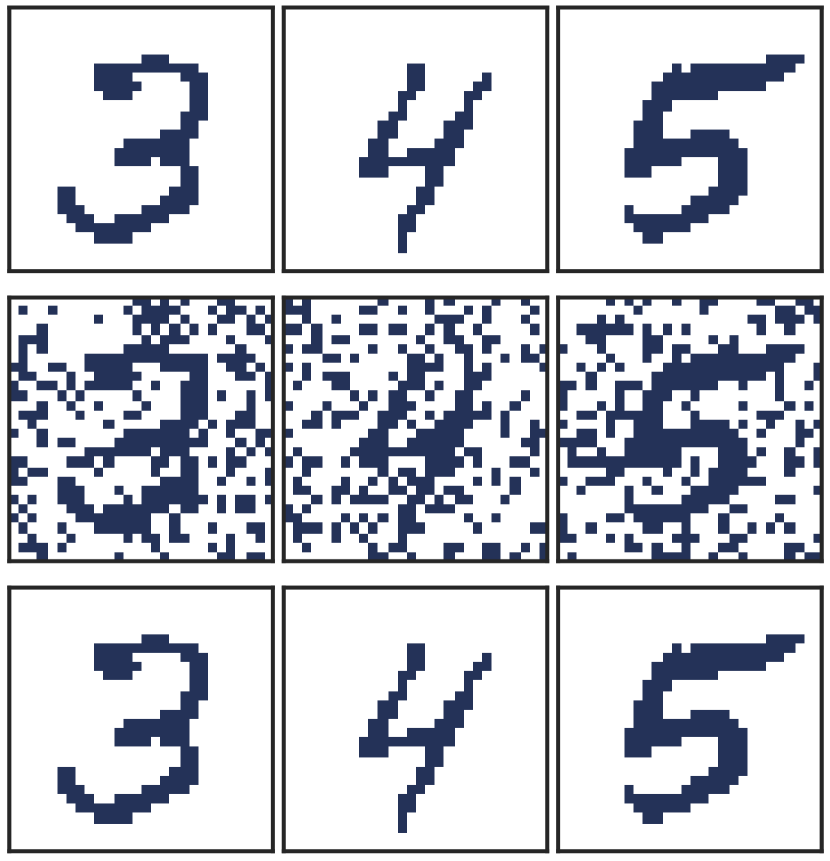
To evaluate the effectiveness of the proposed design in processing associative memory tasks, we conducted systematic experiments using a constructed Hopfield network shown in Fig. 1. We created two Hopfield networks of different scales: 1) 100 neurons and 10 000 synaptic connections for processing binary matrices of 1010 pixels, and 2) 784 neurons and 614 656 synapses for processing the MNIST dataset which has binary matrices of 2828 pixels.
Multiple input patterns with local similarities and well-distributed patterns are employed to evaluate the effect of multiple associative recalls. Fig. 11(a) shows a successful recovery of 100-dimensional pattern vectors which are randomly injected with noise. The memorized patterns, input patterns with 30% noise, and recovered patterns after associative recall are shown separately in this figure. Fig. 11(b) utilizes a relatively larger-scale network to process the MNIST dataset and demonstrates the ability to recover noisy data effectively.
(a)10x10 pixel digits.
(b)MNIST dataset.
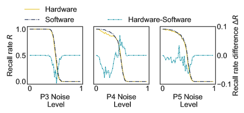
Fig. 12 shows the recall rate for patterns “3”, “4”, and “5” (denoted as P3, P4, P5) with a size of pixels, under different noise levels. The network executed associative recall on input noisy patterns 1 000 times for each noise level to calculate value. Different colored curves represent the recall rates and their variations under software and hardware implementations. The secondary y-axis represents the difference in recall rates between the two implementations . It can be observed that around a noise level of 50%, the recall rate of the hardware implementation is slightly lower than that of the software implementation due to potential errors introduced by representing weights using post-synaptic voltage. In software implementation, the post-synaptic voltage is calculated using precise theoretical values, while in simulated circuits, this value can subject to variations. We performed further analysis on the significant difference between the hardware and software implementations using the Mann-Whitney U test[27]. The Mann-Whitney U test is a non-parametric statistical method used to compare the medians of two independent samples for significant differences. When conducting the test, we first establish the null hypothesis, assuming that there is no significant difference between the two sets of data. By ranking and calculating the ranks of the sample data, we obtain the test statistic U and the calculated p-value is 0.33. Based on the commonly used significance level (typically 0.05), we find that the p-value is greater than 0.05. Therefore, we fail to reject the null hypothesis, indicating that we cannot conclude significant differences in the medians of the two data sets. In other words, the recall effect of Spin-NeuroMem is comparable to the software implementation.
Table 3 compares the recall latency for a single recall task using Spin-NeuroMem and software-based Hopfield networks. The input patterns of the serialized and paralyzed networks use a same noisy 2828 pixel MNIST image. The execution time for a single software associative memory recall is on average when utilizing a single CPU core. The CPU accelerates computations through multi-core parallel processing. A 24-core CPU achieves a speedup compared to a single-core CPU. In contrast, the novel and efficient architecture of Spin-NeuroMem exhibits a gate-level latency of . It achieves a speedup of in associative memory recall compared to its software counterpart running on a single-core CPU.
| single-core CPU | multi-core (24) CPU | Spin-NeuroMem | |
|---|---|---|---|
| recall latency (s) | |||
| speedup |
5 Conclusion
This paper presents Spin-NeuroMem, a low-power neuromorphic associative memory design that integrates spintronic devices and CMOS components. The experimental results show superior performance of this design in terms of power consumption and area, particularly with increasing weight scale. Moreover, our proposed Spin-NeuroMem can achieve a recall rate on par with that of software-based Hopfield networks while showcasing a significant improvement in speed. Overall, our work demonstrates the potential of spintronic neural network hardware for building next-generation neural computing platforms.
It is important to highlight that there are still potential challenges that need to be addressed in the utilization of spintronic devices in neuromorphic computing. The Magnetic Tunnel Junctions (MTJs) employed for binary data storage remain unable to accurately represent continuous weight changes, thereby restricting the range of intelligent tasks networks can undertake. Furthermore, manufacturing limitations on TMR and additional production challenges associated with enhancing TMR, including constraints on serial transistors and size, necessitate more comprehensive discussion and resolution.
References
References
- [1] Amrouch H, Chen J J, Roy K, Xie Y, Chakraborty I, Huangfu W, Liang L, Tu F, Wang C and Yayla M 2021 Brain-Inspired Computing: Adventure from Beyond CMOS Technologies to Beyond von Neumann Architectures ICCAD Special Session Paper ICCAD pp 1–9 doi: 10.1109/ICCAD51958.2021.9643488
- [2] Marković D, Mizrahi A, Querlioz D and Grollier J 2020 Nat. Rev. Phys. 2 499–510 doi: 10.1038/s42254-020-0208-2
- [3] Hopfield J J and Tank D W 1986 Science 233 625–633 doi: 10.1126/science.3755256
- [4] Hu S G, Liu Y, Liu Z, Chen T P, Wang J J, Yu Q, Deng L J, Yin Y and Hosaka S 2015 Nat. Commun. 6 7522 doi: 10.1038/ncomms8522
- [5] Li Y, Wang Z, Midya R, Xia Q and Yang J J 2018 J. Phys. D: Appl. Phys. 51 503002 doi: 10.1088/1361-6463/aade3f
- [6] Telminov O and Gornev E 2022 Possibilities and Limitations of Memristor Crossbars for Neuromorphic Computing 2022 6th Scientific School Dyn. Complex Networks and their Appl. (DCNA) pp 278–281 doi: 10.1109/DCNA56428.2022.9923302
- [7] Jang J, Lee S and Park W 2023 IEEE Trans. Magn. 59 1–5 doi: 10.1109/TMAG.2023.3288546
- [8] Zhang D, Zeng L, Cao K, Wang M, Peng S, Zhang Y, Zhang Y, Klein J O, Wang Y and Zhao W 2016 IEEE Trans. Biomed. Circuits Syst. 10 828–836 doi: 10.1109/TBCAS.2016.2533798
- [9] Fukami S and Ohno H 2018 J. Appl. Phys. 124 151904 doi: 10.1063/1.5042317
- [10] Amirany A, Moaiyeri M H and Jafari K 2020 IEEE TETC 10 428–437 doi: 10.1109/TETC.2020.3026179
- [11] Fu S, Li T, Zhang C, Li H, Ma S, Zhang J, Zhang R and Wu L 2023 IEEE TVLSI Syst. 31 1578–1591 doi: 10.1109/TVLSI.2023.3298327
- [12] Gallagher W J and Parkin S S P 2006 IBM J. Res. Dev. 50 5–23 doi: 10.1147/rd.501.0005
- [13] Chen J Y, Feng J F and Coey J M D 2012 Appl. Phys. Lett. 100 142407 doi: 10.1063/1.3701277
- [14] Chen J Y, Carroll N, Feng J F and Coey J M D 2012 Appl. Phys. Lett. 101 262402 doi: 10.1063/1.4773180
- [15] Ikeda S, Hayakawa J, Lee Y M, Matsukura F, Ohno Y, Hanyu T and Ohno H 2007 IEEE Trans. Electron Devices 54 991–1002 doi: 10.1109/TED.2007.894617
- [16] Yuasa S, Hono K, Hu G and Worledge D C 2018 MRS Bull. 43 352–357 doi: 10.1557/mrs.2018.93
- [17] Mathon J and Umerski A 2001 Phys. Rev. B 63 220403 doi: 10.1103/PhysRevB.63.220403
- [18] Sato N, Allen G A, Benson W P, Buford B, Chakraborty A, Christenson M, Gosavi T A, Heil P E, Kabir N A, Krist B J, O’Brien K P, Oguz K, Patil R R, Pellegren J, Smith A K, Walker E S, Hentges P J, Metz M V, Seth M, Turkot B, Wiegand C J, Yoo H J and Young I A 2020 CMOS compatible process integration of SOT-MRAM with heavy-metal bi-layer bottom electrode and 10ns field-free SOT switching with STT assist IEEE Symp. VLSI Technol. pp 1–2 doi: 10.1109/VLSITechnology18217.2020.9265028
- [19] Carboni R, Ambrogio S, Chen W, Siddik M, Harms J, Lyle A, Kula W, Sandhu G and Ielmini D 2018 IEEE IEDM 65 2470–2478 doi: 10.1109/TED.2018.2822343
- [20] Cai F, Kumar S, Van Vaerenbergh T, Sheng X, Liu R, Li C, Liu Z, Foltin M, Yu S, Xia Q, Yang J J, Beausoleil R, Lu W D and Strachan J P 2020 Nat. Electron. 3 409–418 doi: 10.1038/s41928-020-0436-6
- [21] Ebong I E and Mazumder P 2011 IEEE Trans. Nanotechnol. 10 1454–1463 doi: 10.1109/TNANO.2011.2166805
- [22] Saadeldeen H, Franklin D, Long G, Hill C, Browne A, Strukov D, Sherwood T and Chong F T 2013 Memristors for Neural Branch Prediction: A Case Study in Strict Latency and Write Endurance Challenges Acm Int. Conf. Comput. Frontiers CF ’13 (New York, NY, USA: Association for Computing Machinery) ISBN 9781450320535 doi: 10.1145/2482767.2482801
- [23] YAN A, LAI C, ZHANG Y, Cui J, Huang Z, SONG J, Guo J and Wen X 2021 IEEE TETC 9 520–533 doi: 10.1109/TETC.2018.2871861
- [24] LeCun 1998 http://yann. lecun. com/exdb/mnist/
- [25] Wang M, Cai W, Cao K, Zhou J, Wrona J, Peng S, Yang H, Wei J, Kang W, Zhang Y, Langer J, Ocker B, Fert A and Zhao W 2018 Nat. Commun. 9 671 doi: 10.1038/s41467-018-03140-z
- [26] Wu L, Rao S, Taouil M, Marinissen E J, Kar G S and Hamdioui S 2022 IEEE TCAD 41 4991–5004 doi: 10.1109/TCAD.2021.3140157
- [27] MacFarland T W and Yates J M 2016 Mann–Whitney U Test (Cham: Springer) pp 103–132 ISBN 978-3-319-30634-6 doi: 10.1007/978-3-319-30634-6_4