Quadratic optical response of CrSBr controlled by spin-selective interlayer coupling
Abstract
The optical properties of the layered magnet CrSBr are dominated by intralayer excitons: the antiferromagnetic order between the layers makes layer-to-layer charge hopping, and therefore interlayer excitons, spin-forbidden. An external magnetic field, however, continuously drives the magnetic order towards layer-to-layer ferromagnetic, which opens spin-allowed charge-transfer channels between the layers. Here we elaborate how their admixture changes the composition and nature of the excitons, leading to an extension over many layers, and causes a quadratic red-shift with respect to the external magnetic field. We address these effects by ab-initio -BSE calculations as a function of magnetic field and cast the data into a minimal four-band model to elucidate the interplay between the various interaction and coupling mechanisms. Our findings should be generally valid for antiferromagnetic layered magnets with and without external magnetic fields, and moreover for any couple of layers with different spin directions. Our insights help to systematically address excitons and predict their optical signatures in such systems.
Introduction.
Manipulating material properties via external stimuli like screening, moiré traps, or magnetism is a key focus in basic research due to its easy tunability of opto-electronics Wang et al. (2017); Huang et al. (2022); Zhao et al. (2017); Jauregui et al. (2019). The influence of magnetism, particularly in 2D magnets like CrI3 and CrSBr, offers a practical way to control their quantum states Wu et al. (2019); Klein et al. (2019); Gibertini et al. (2019). In van der Waals (vdW) layered crystals, such as easily exfoliatable semiconductors that form moiré patterns of two-dimensional (2D) stacked heterostructures Gong et al. (2014); Liu et al. (2014); Huang et al. (2022); Cao et al. (2018) or magnetically controlled valley excitons Heißenbüttel et al. (2021); Seyler et al. (2018), understanding interlayer coupling mechanisms is crucial for further development of the intricate field of integrated systems with a variety of applications in ultracompact information technology Deng et al. (2022) or even synaptic devices Sun et al. (2020). Recent work by Wilson et al. Wilson et al. (2021) revealed a magnetic control mechanism for excitons in antiferromagnetic (AFM) bilayer CrSBr, where the magnetization direction affects exciton energies and wavefunctions. CrSBr, with its semiconducting electronics, large crystal anisotropy, and vdW coupled AFM stacked layers, exhibits intriguing phenomena, especially air-stability, high Nèel- and Curie-temperatures of 132 K and 160 K, respectively, or 1D electronics and optics Göser et al. (1990); Klein et al. (2023); Lee et al. (2021); Telford et al. (2020) and is a perfect playground for experiments on magnetism and correlated phenomena in two or three dimensions. When the magnetic moments are rotated from an AFM coupling in-plane to a FM coupling parallel to the external magnetic field, the lowest exciton in experiments exhibit a quadratic redshift and its wavefunction gains significant charge transfer (CT) Wilson et al. (2021); Tabataba-Vakili et al. (2023). Such a quadratic response is in sharp contrast to the linear -factors due to the Zeeman shift in common materials Li et al. (2014); Aivazian et al. (2015); Srivastava et al. (2015); Arora et al. (2016); Deilmann et al. (2020). This provides a manageable technique to control excitons in future devices and even switch them to CT excitons with an out-of-plane dipole. Our experimental and first principles -BSE data match very well, and we are able to develop a general model offering deep insights into the magnetic phase dependent physics involved. The influence of the external magnetic field on CrSBr is expressed well in our model and we can reproduce and quantify the redshift of exciton energies and increasing CT character. Despite its simplicity, the proposed model is generally applicable to coupled 2D magnets. Additionally, our studies unveil that a symmetry forbidden, dark exciton is the lowest in energy at finite external magnetic fields. These findings not only enhance our understanding of analogous systems but also open avenues for applications with precise control over switching mechanisms.
Results.
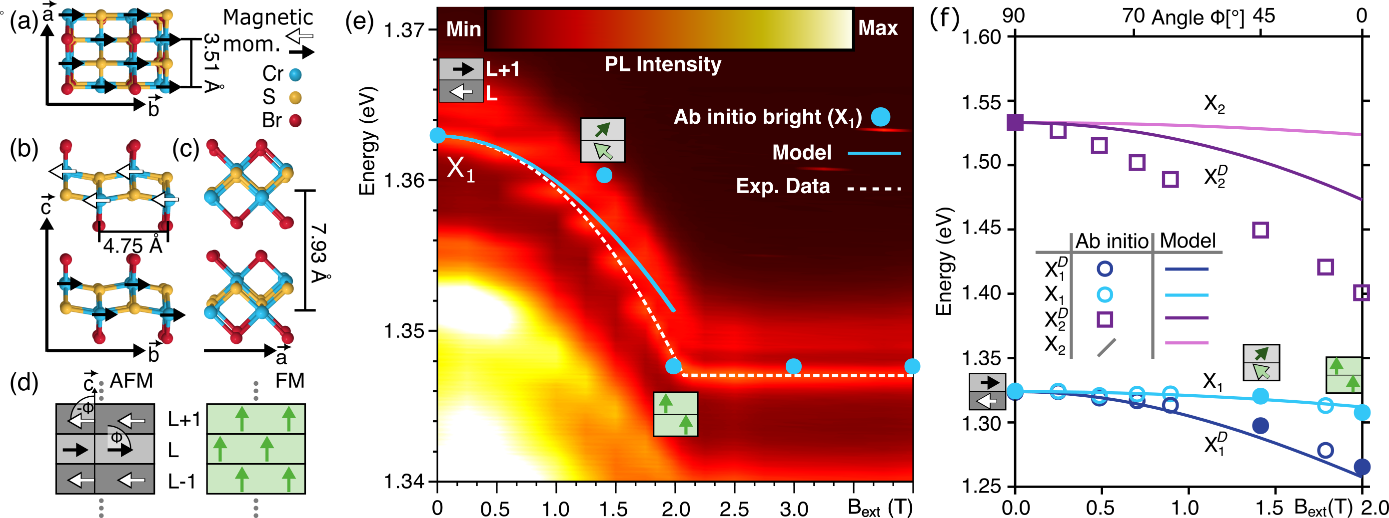
We study a multilayer of CrSBr evolving from the layered in-plane AFM order into an external field induced out-of-plane FM order. In Fig. 1 (a)-(d) the crystal and magnetic structure of AFM and FM CrSBr is sketched. Each layer consists of two inner planes of alternating chromium and sulfur atoms embedded in two layers of out-stacking bromine atoms. The magnetic moments of 3.3 µ from theory are hosted at each chromium atom and align ferromagnetically along the crystal easy axis b. A triaxial, anisotropic behavior with hard, middle and easy magnetization axis along c, a, and b, respectively Yang et al. (2021) leads to large magnetic, electronic and optical anisotropy, one-dimensional electronics and cigar-like 1D excitons with large binding energy even in bulk material Klein et al. (2023). Vertically, the monolayers are arranged in AFM A-stacking. Due to the magnetic order, only the combination of time-reversal and inversion symmetry is preserved in the AFM multilayer leading to the space group.
An external magnetic field perpendicular to the layers changes the magnetization continuously from AFM into FM order (see Fig. 1 (d)). For complete rotation from in-plane AFM (along b) to FM (along c), the external field has to overcome the magnetic anisotropy and AFM coupling energy. A clear signature of this changed spin arrangement is given by our photoluminescence (PL) data at low temperature (4 K) in Fig. 1 (e), in which we observe a quadratic redshift of the lowest exciton marked by the dashed black line starting at 1.362 eV (AFM) proceeding to 1.347 eV (FM). Note that the broad PL intensity at lower energies may not be attributed to excitons and originates most likely from self-hybridized polaritons Wang et al. (2023); Dirnberger et al. (2023) or similar, and is therefore not of interest in the scope of this work.
The key issue of our present work is to understand the relationship between external magnetic field, rotation of the magnetic moments, and its effect on the excitons. To this end, we first calculate the electronic and excitonic states from first principles (-BSE calculations in Fig. 1 (f) (dots)) at various intermediate tilting angles (see Fig. 1 (d) for the definition of ) and then condense the findings and mechanisms into a minimal model.
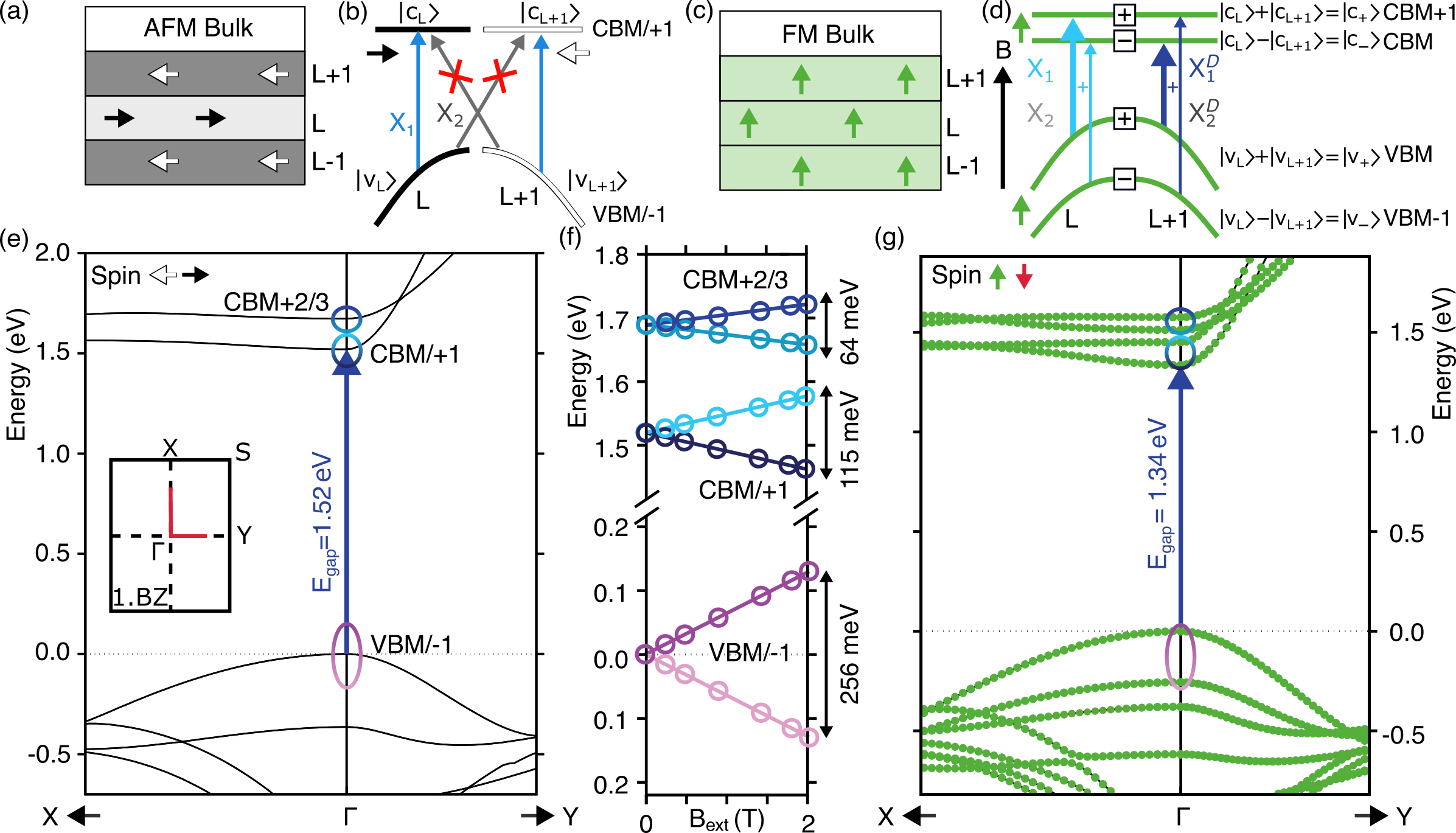
Each angle of magnetic moments is attributed to the strength of the external magnetic field between T (AFM) up to the saturation magnetization of about T (FM). The field gradually forces the moments to align parallel to it ( c) and tilts moments of adjacent layers parallel to each other. The magnetization direction in CrSBr is determined by a minimum in total magnetic energy for a given external field. This is given by three terms: the antiferromagnetic exchange coupling of adjacent layers , the crystal anisotropy energy , and the Zeeman energy that prefers moments parallel aligned to the external field (for details see Supplementary Information (SI) \bibnotemark[Supplement]). \bibnotetext[Supplement]Supplementary Information at link for details on sample preparation, magnetic switching process and model development as well as on the ab initio data. Minimization with respect to the external magnetic field yields that the tilting angle is given by . At and beyond the saturation field strength , ferromagnetic order () is achieved. Our PL data of Fig. 1 (e) show that 2.0 T. For neighboring layers exhibit alternating orientation of their magnetic moments (L ; L , see Fig. 1 (d).) In the AFM state () CrSBr consists of two alternating layer types, L with moments of the majority spin channel along b and L along b. For our discussions only the character of states close to the electronic gap, which are determined by the majority spin channel, are relevant (states of the minority channel are more than eV away from the gap). Moreover, for these states of interest a very small spin orbit coupling (SOC) is found, so that the AFM crystal has entirely decoupled layers with electrons on neighboring layers quasi orthogonal in their spin direction.
Our calculations find two lowest-energy excitons at about 1.3 eV. In the AFM case () the perfect orthogonality between the spin channels of neighboring layers causes perfect intralayer nature (i.e., electron and hole reside on the same layer) and degeneracy of the two excitons (at 1.324 eV). Through the external field and the gradually parallel spin alignment the spin orthogonality is lost and coupling of layers becomes possible. With increasing the two excitons split into a bright upper state X1 and an optically forbidden, dark lower state X (blue dots and lines in Fig. 1 (f)). They are shifted quadratically down in energy, finally reaching eV (X) and eV (X1) in FM order at saturation field strength. The state X1 is clearly observed in the measured PL data of Fig. 1 (e), with the same energy downshift of 15 meV from AFM to FM. Here, our ab intio data for the redshift agree perfectly with the experiment which is even at quantitative level suprisingly good. The energetically lower, dark X with a larger calculated redshift ( meV) is not observed in the PL data. We aim to understand and model the detailed physical mechanisms that control all effects resulting from the tuned interaction of layers. To keep this model as simple as possible we will consider only transitions between the two highest valence and two lowest conduction bands.
Electronic properties and linear shift.
To understand the influence of the magnetization direction on the excitons, we have to look firstly at the single-particle physics of the electrons and holes from which the excitons are formed. Fig. 2 shows the dependence of the electronic states from on the magnetic field for the two extreme cases AFM (e), FM (g) and the explicit dependence on the field strength (f). For our exciton analysis only the two highest valence and two lowest conduction bands are relevant. The AFM order (Fig. 2 (e)) has a direct band gap of eV at with nearly dispersionless bands along -X resulting from crystal anisotropy as presented before Klein et al. (2023). Each line denotes two spin-degenerate states, with each state about 99% polarized along b/b. As mentioned, due to the very small SOC, all of these states stem from the majority spin channel of the two layer types. In AFM order, the electron wavefunctions of adjacent layers are spin-orthogonal and the electrons cannot tunnel to neighboring layers. At finite the moments are tilted (), and the spin states get a component along , i.e. perpendicular to the layers (for details see SI). This causes interlayer interaction and splitting of the formerly degenerate states, proportional to . Fig. 2 (f) shows our calculated energy shifts at . For full FM order (at and beyond T) we find splittings of and meV for VBM/VBM and CBM/CBM, respectively. In the saturated FM configuration all bands are spin polarized vertically to the layers, the direct gap reduces to eV at and dispersions along -X are enhanced (Fig. 2 (g)).
A simple model allows to describe the influence of the layer coupling on the electrons and thus reproduces our results. We introduce a coupling Hamiltonian in the electronic basis states on layer L and L (see Fig. 2 (b)). The coupling strength is proportional to the parallel aligned spin component (i.e. , for details see SI) while the proportionality constant is given by the finite overlap of the spatial wavefunctions. For each pair of degenerate bands this leads to a coupling Hamiltonian
| (1) |
From the bandstructure (Fig. 2 (g)) we find that all quantities are dependent. Here, is the degenerate eigenenergy of state in the AFM order and is the coupling strength or tunneling parameter of a particle between L and L. The diagonalization leads to eigenenergies and wavefunctions which are the corresponding positive and negative linear combinations of bands from each single layer, denoted in Fig. 2 (d) e.g. (details see SI). From the linear fit of our ab initio data at in Fig. 2 (f) we get the parameters of the VBM meV/T and the CBM meV/T for a hole/electron at , respectively.
Optical properties and quadratic shift.
Having understood the coupling of electronic states, we get back to the behavior of excitons in Figs. 1 (e) and (f). In the absence of interlayer coupling (AFM) the first degenerate exciton pair is at eV. We can describe these states in two different ways. Either we explain them as transitions of an electron from the VBM to the CBM on each layer, L or L+1 seperately (Fig. 2 (b)), or we use the combined basis of and (see Fig. 2 (d) with zero splitting), which is convenient for but also for T. Four transitions , , , and ) are possible between these states. Due to the symmetry of the system (i.e. Klein et al. (2023) the first two and last two transitions do not mix (see SI). Here, we focus on and which results in a Hamiltonian for the bright excitons. The other two transitions can be treated analogously.
| (2) |
Neglecting the electron-hole interaction and the diagonal would describe uncorrelated interband transitions between the bands, i.e. the gap energy and its shift by the combined tunneling parameters of electron and hole . The electron-hole interaction enters on the diagonal, while the off-diagonal is given by the difference of intralayer () and interlayer () interaction for electron and hole on the same (IN) and different layers (CT), respectively. We underline that only the energy splitting of the bands changes with , whereas the electron-hole interaction is constant. Nevertheless, its effect on the excitonic states varies with and results in changes of the exciton energy and its character as we show in our analysis of states below. From the previous considerations in Eq. (1) on the basis of ab-initio we use and including the -dependence of points in the crystal direction, with being the number of grid points in that direction to be employed in the BSE calculation for the excitons. From our ab-initio BSE we find and .
The diagonalization of Eq. (Optical properties and quadratic shift.) yields the dominant behavior of the exciton energies
and mixes the corresponding transitions and to X1,2.
From our ab initio data we find X2 at eV in the AFM state shifting to eV in the FM state (see Fig. 1 (f)).
For the symmetry forbidden, dark transitions (,) the Hamiltonian looks similar to Eq. (Optical properties and quadratic shift.) with one important distinction:
Instead of the difference of tunneling enters.
The corresponding excitons X and X are lower in energy compared to their bright counterparts (see Fig. 1 (f)).
With increasing , X and X1 split due to the different tunnelings and decreasing gaps of and .
Considering the simplicity of the model, the agreement with the ab-initio /BSE results
(circles/squares in Fig. 1 (f)) is very good, especially for the lowest states.
The model fully explains the experimentally measured redshift in Fig. 1 (b)) of X1.
The nature of the excitons is governed by the relative alignment of the spins
which leads to the different tunnelings and .
For a better understanding, we analyse their character in the following.
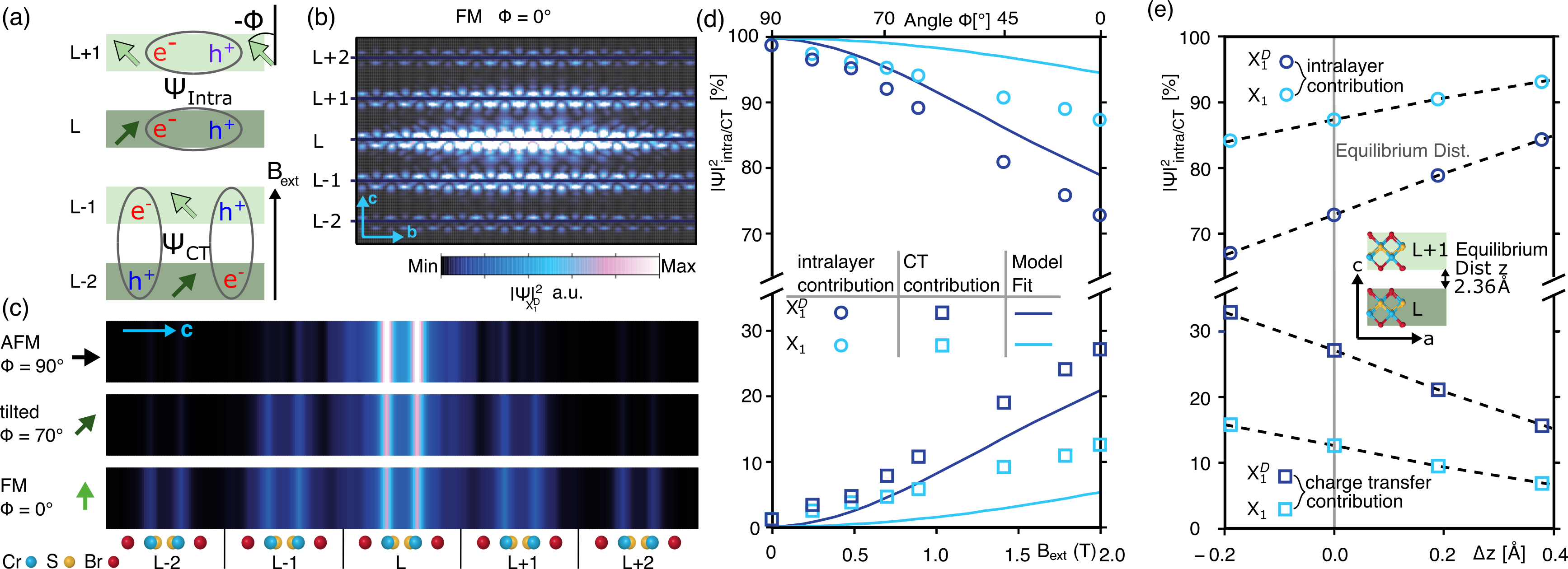
Controlling the charge transfer contribution.
The basis of and is symmetric on both layers, L and L+1, and may hide the localization of each exciton at first glance. Thus, in Fig. 3 we analyze the internal structure of the excitons. Panels (b) and (c) show the probability distribution of the electron relative to the hole (located on the middle layer), for the state X (the state X1 looks similar). The lowest excitons of CrSBr are influenced by the large crystal anisotropy and the flat bands along -X lead to extended 1D like exciton wavefunctions along axis b (Fig. 3 (b)). When the external magnetic field is turned on, the enabled layer interaction induces hopping of the electron from layer L (position of the hole) to layer L1 and farther. In Fig. 3 (c) we show the projection of the exciton wavefunction onto the axis c, evolving from being restricted to one layer to becoming more extended to the adjacent layers with increasing tilting angle. In the AFM state the exciton is fixed to layer L and its character is intralayer while in the FM state the exciton is extended and gets significant charge transfer contributions. For the analysis of this CT of X and X1 we sum up the probability density on the layer with the hole (intralayer) and the probability on the adjacent layers (CT) and give the percentages in Fig. 3 (d). The ab initio results (dots) at T show decoupled layers, where both excitons are vertically restricted to the respective layer (99% intralayer character). With increasing magnetic field we find that the states get a significant CT with up to 27% (X) and 13% (X1) in the FM order.
From our minimal model the contributions can be evaluated as sum and difference of the two evolved transitions. E.g. for the contributions of and are identical, their sum (intralayer contribution) is 1, their difference (CT contribution) is zero. Qualitatively we find the same behavior with increasing as in our ab initio results shown as the blue curves in Fig. 3 (d). To first non-vanishing order in the model yields the CT contribution and explains the smaller contribution of X1 () compared to X (). In saturation we find 21% (X) and 5% (X1) CT which is similar to the ab initio results discussed above. Thus the energetically lowest excitons remain intralayer type with significant CT contributions at finite fields. The higher-energy excitons X and X2 (1.533 eV in AFM order) show the opposite behavior, starting at 100% CT character and gaining some intralayer share towards FM.
This analysis fully explains the increasing CT admixture of and observed in our ab-initio data. Quantitative agreement, however, is not achieved (see e.g. Fig. 3 (d)) due to the minimal nature of our model (e.g., the number of bands included).
These findings suggest further ways to manipulate the energy and CT character in CrSBr.
With a variation of the layer distance we can change the overlap of orbitals (mostly given by Br atoms) that mediate the interlayer interaction and thus the size of tunneling .
In Fig. 3 (e) we show the dependence of the CT contribution to X/X1 on the relative variation of layer distance with respect to the equilibrium position.
If the distance is compressed by 0.2 Å, the CT contribution is increased from 27% to 33%, while a lattice expansion by 0.2 Å leads to 21% CT contribution to the X (for details see SI).
In experiment the interlayer distance may be controlled e.g. by pressure as done in Pawbake et al. (2023) and our findings can explain excitonic behavior under such conditions.
In summary, we explain the underlying mechanisms governing the behavior of electrons and excitons in multilayer CrSBr under the influence of an external magnetic field. Our ab initio -BSE calculations accurately reproduce the redshift of the lowest visible exciton and reveal a splitting of formerly spin-degenerate states, proportional to the magnetic field. The energy redshifts, CT admixture, and band gap reduction are explained well in our simple but expressive model set up by parameters from the ab-initio data. External magnetic fields enable the layer coupling and induce a substantial CT character of the excitons of up to 27% in the ferromagnetic order, which is further manipulable by adjusting the interlayer distance. Of particular interest is the identification of a dark symmetry-forbidden exciton state initially degenerate with the allowed second exciton in the antiferromagnetic crystal. This state, shifts to energies below the visible bright exciton observed in photoluminescence at finite fields. Our findings pave the way for a systematic control of electrons, excitons, charge transfer dynamics, vertical extension of wavefunctions, and binding energies through the application of external magnetic fields.
METHODS
Experimental characterization and photoluminescence spectroscopy
Bulk-like multilayer samples of CrSBr have been prepared by micromechanical cleavage from bulk crystals onto SiO2/Si substrates using Nitto tape. The thickness of nm and nm of the multilayer flakes has been determined by atomic force microscopy in ambient using a XE 100 from Park Systems with a cantilever of the NSC 15 series in the non-contact mode. The samples are characterized by non-resonant Raman spectroscopy using linearly polarized light from a 532 nm (2.33 eV) wavelength laser diode. In order to determine the in-plane crystallographic a and b directions that are highly anisotropic, the linearly polarized light in the excitation path has been rotated with respect to the crystal axes and the co-linear polarized Raman response has been determined. The intensity of first order Raman modes are sensitive to the crystallographic direction Klein et al. (2023). Our magneto-photoluminescence measurements were conducted at 4 K in Faraday configuration utilizing a pulse tube refrigeration operating with helium gas (Bluefors) equipped with windows for optical access and with a superconducting 7 T electromagnet. The sample was mounted on a cold finger equipped with piezo stages for sub-micrometer positioning accuracy. The laser was focused on the sample in back-scattering geometry with a low temperature compatible objective lense with a numerical aperture of 0.82 mounted on a homebuilt stage attached to the 4 K stage of the cryostat. The focused spot on the sample had a diameter of µm in the relevant wavelength range. The sample was excited close to resonance at a wavelength of 850 nm (1.46 eV) using a continuously frequency tunable continuous wave (CW) Ti:sapphire laser. The emitted light was guided to the entrance slit of a spectrometer with 750 nm focal length and dispersed using a 600 lines/mm grating resulting in a spectral resolution of 0.1 nm within the relevant wavelength range of 900 nm to 950 nm.
Many body perturbation theory from the and BSE scheme
To simulate the experimental samples we study bulk CrSBr. The description requires arbitrary spin configurations, i.e. in-plane ferromagnetic order, antiferromagnetic order from adjacent layers, and different tilted spin configuration in between. We cannot neglect spin-orbit coupling effects although the effects for the states close to the gap are small. For energetically higher and lower states, as well as for the correct description of symmetry in this system, spin-orbit coupling is taken fully into account. Therefore, we calculated the electronic ground state from first principles by employing density functional theory (DFT) in the noncollinear formalism of the spin density approach Stärk et al. (2011); Sandratskii (1998). For the exchange correlation functional we applied the generalized gradient approximation (GGA) Perdew et al. (1992). The resulting energies and spinor wavefunctions are used as a starting point for many body perturbation theory including the noncollinear magnetism and spin-orbit coupling effects. In the approximation Hedin (1965) we calculated the self-energy from the one-particle Green’s function and the screened Coulomb interaction (including the dielectric response in random phase approximation) which is then used to calculate the quasiparticle (QP) bandstructures. Here, replaces the DFT exchange correlation energy and leads to the QP Hamiltonian and eigenenergies
| (3) | ||||
| (4) |
While we do not extend our DFT description by adding an arbitrary Hubbard , we note the related physical effects like on-site Coulomb repulsion and Hubbard correlation are included in the self-energy. In this QP approach we employ the so-called one-shot method including non-diagonal terms of the self-energy as we have previously found that the diagonal parts are not sufficient for CrSBr Deilmann (2020); Heißenbüttel et al. (2021); Förster et al. (2015). The solution of the full eigenvalue problem yields the coefficients for the linear combination of DFT states to the new QP wavefunctions (for details see Ref. Heißenbüttel et al. (2021))
| (5) | ||||
| (6) |
To anticipate the large opening of the band gap from DFT to QP bandstructure and to circumvent a full self-consistent to determine the shifts we applied a scissors operator of 1.0 eV.
To evaluate the optical behavior of CrSBr including the electron-hole interaction we solve the Bethe-Salpeter equation (BSE) Rohlfing and Louie (2000) on top of the approximation. For exciton state this is given by
| (7) |
with the interaction kernal in Tamm-Dancoff approximation, the energy of exciton state and the amplitudes that set up the exciton wavefunctions
| (8) |
Here, is the combination of position and spin and the results from Fig. 3 correspond to .
We include the off-diagonal elements of the self-energy as the BSE is solved in the original DFT basis as explained in details in Ref. Heißenbüttel et al. (2021).
For our quasiparticle calculations we employ a hybrid basis set of Gaussian orbitals with decay constants from 0.14 to 12.5 a-2 combined with plane waves with an energy cutoff set to 1.5 Ry
to represent of all two-point functions () in .
Moreover, we apply a -point sampling of points in the first Brillouin zone for well converged results and use, due to the numerical costs for the BSE, a grid of points, which is sufficiently converged for the lowest exciton states.
AUTHOR INFORMATION
Corresponding Author
Marie-Christin Heißenbüttel – Institute of solid state theory, University of Münster, 48149 Münster, Germany
Authors
Pierre Piel – Physical institute, University of Münster, 48149 Münster, Germany
Julian Klein – Department of Materials Science and Engineering, Massachusetts Institute of Technology, Cambridge, MA 02139, USA
Thorsten Deilmann – Institute of solid state theory, University of Münster, 48149 Münster, Germany
Ursula Wurstbauer – Physical institute, University of Münster, 48149 Münster, Germany
Michael Rohlfing – Institute of solid state theory, University of Münster, 48149 Münster, Germany
Notes
The authors declare no competing financial interest.
Acknowledgements.
The authors gratefully acknowledge the financial support from German Research Foundation (DFG Project No. DE 2749/2-1 and No. WU637/4-2, 7-1), the DFG Collaborative Research Center SFB 1083 (Project No. A13), and computing time granted by the John von Neumann Institute for Computing (NIC) and provided on the super-computer JUWELS at Jülich Supercomputing Centre (JSC).REFERENCES
References
- Wang et al. (2017) Yuan Wang, Shuai Zhang, Di Huang, Jingxin Cheng, Yingguo Li, and Shiwei Wu, “Screening effect of graphite and bilayer graphene on excitons in MoSe2 monolayer,” 2D Materials 4, 015021 (2017).
- Huang et al. (2022) Di Huang, Junho Choi, Chih-Kang Shih, and Xiaoqin Li, “Excitons in semiconductor moirésuperlattices,” Nature Nanotechnology 17, 227–238 (2022).
- Zhao et al. (2017) Chuan Zhao, Tenzin Norden, Peiyao Zhang, Puqin Zhao, Yingchun Cheng, Fan Sun, James P. Parry, Payam Taheri, Jieqiong Wang, Yihang Yang, Thomas Scrace, Kaifei Kang, Sen Yang, Guo-xing Miao, Renat Sabirianov, George Kioseoglou, Wei Huang, Athos Petrou, and Hao Zeng, “Enhanced valley splitting in monolayer WSe2 due to magnetic exchange field,” Nature Nanotechnology 12, 757–762 (2017).
- Jauregui et al. (2019) Luis A. Jauregui, Andrew Y. Joe, Kateryna Pistunova, Dominik S. Wild, Alexander A. High, You Zhou, Giovanni Scuri, Kristiaan De Greve, Andrey Sushko, Che-Hang Yu, Takashi Taniguchi, Kenji Watanabe, Daniel J. Needleman, Mikhail D. Lukin, Hongkun Park, and Philip Kim, “Electrical control of interlayer exciton dynamics in atomically thin heterostructures,” Science 366, 870–875 (2019).
- Wu et al. (2019) Meng Wu, Zhenglu Li, Ting Cao, and Steven G. Louie, “Physical origin of giant excitonic and magneto-optical responses in two-dimensional ferromagnetic insulators,” Nature Communications 10, 2371 (2019).
- Klein et al. (2019) Dahlia R. Klein, David MacNeill, Qian Song, Daniel T. Larson, Shiang Fang, Mingyu Xu, R. A. Ribeiro, P. C. Canfield, Efthimios Kaxiras, Riccardo Comin, and Pablo Jarillo-Herrero, “Enhancement of interlayer exchange in an ultrathin two-dimensional magnet,” Nature Physics 15, 1255–1260 (2019).
- Gibertini et al. (2019) M. Gibertini, M. Koperski, A. F. Morpurgo, and K. S. Novoselov, “Magnetic 2D materials and heterostructures,” Nature Nanotechnology 14, 408–419 (2019).
- Gong et al. (2014) Yongji Gong, Junhao Lin, Xingli Wang, Gang Shi, Sidong Lei, Zhong Lin, Xiaolong Zou, Gonglan Ye, Robert Vajtai, Boris I. Yakobson, Humberto Terrones, Mauricio Terrones, Beng Kang Tay, Jun Lou, Sokrates T. Pantelides, Zheng Liu, Wu Zhou, and Pulickel M. Ajayan, “Vertical and in-plane heterostructures from WS2/MoS2 monolayers,” Nature Materials 13, 1135–1142 (2014).
- Liu et al. (2014) Kaihui Liu, Liming Zhang, Ting Cao, Chenhao Jin, Diana Qiu, Qin Zhou, Alex Zettl, Peidong Yang, Steve G. Louie, and Feng Wang, “Evolution of interlayer coupling in twisted molybdenum disulfide bilayers,” Nature Communications 5, 4966 (2014).
- Cao et al. (2018) Yuan Cao, Valla Fatemi, Ahmet Demir, Shiang Fang, Spencer L. Tomarken, Jason Y. Luo, Javier D. Sanchez-Yamagishi, Kenji Watanabe, Takashi Taniguchi, Efthimios Kaxiras, Ray C. Ashoori, and Pablo Jarillo-Herrero, “Correlated insulator behaviour at half-filling in magic-angle graphene superlattices,” Nature 556, 80–84 (2018).
- Heißenbüttel et al. (2021) Marie-Christin Heißenbüttel, Thorsten Deilmann, Peter Krüger, and Michael Rohlfing, “Valley-dependent interlayer excitons in magnetic WSe2/CrI3,” Nano Letters 21, 5173–5178 (2021).
- Seyler et al. (2018) Kyle L. Seyler, Ding Zhong, Bevin Huang, Xiayu Linpeng, Nathan P. Wilson, Takashi Taniguchi, Kenji Watanabe, Wang Yao, Di Xiao, Michael A. McGuire, Kai-Mei C. Fu, and Xiaodong Xu, “Valley Manipulation by Optically Tuning the Magnetic Proximity Effect in WSe2/CrI3 Heterostructures,” Nano Letters 18, 3823–3828 (2018).
- Deng et al. (2022) Wenjie Deng, Zilong Zheng, Jingzhen Li, Rongkun Zhou, Xiaoqing Chen, Dehui Zhang, Yue Lu, Chongwu Wang, Congya You, Songyu Li, Ling Sun, Yi Wu, Xuhong Li, Boxing An, Zheng Liu, Qi jie Wang, Xiangfeng Duan, and Yongzhe Zhang, “Electrically tunable two-dimensional heterojunctions for miniaturized near-infrared spectrometers,” Nature Communications 13, 4627 (2022).
- Sun et al. (2020) Linfeng Sun, Wei Wang, and Heejun Yang, “Recent progress in synaptic devices based on 2D materials,” Advanced Intelligent Systems 2, 1900167 (2020).
- Wilson et al. (2021) Nathan P Wilson, Kihong Lee, John Cenker, Kaichen Xie, Avalon H Dismukes, Evan J Telford, Jordan Fonseca, Shivesh Sivakumar, Cory Dean, Ting Cao, et al., “Interlayer electronic coupling on demand in a 2D magnetic semiconductor,” Nature Materials 20, 1657–1662 (2021).
- Göser et al. (1990) O. Göser, W. Paul, and H. G. Kahle, “Magnetic properties of CrSBr,” Journal of Magnetism and Magnetic Materials 92, 129–136 (1990).
- Klein et al. (2023) Julian Klein, Benjamin Pingault, Matthias Florian, Marie-Christin Heißenbüttel, Alexander Steinhoff, Zhigang Song, Kierstin Torres, Florian Dirnberger, Jonathan B. Curtis, Mads Weile, Aubrey Penn, Thorsten Deilmann, Rami Dana, Rezlind Bushati, Jiamin Quan, Jan Luxa, Zdeněk Sofer, Andrea Alù, Vinod M. Menon, Ursula Wurstbauer, Michael Rohlfing, Prineha Narang, Marko Lončar, and Frances M. Ross, “The bulk van der waals layered magnet CrSBr is a Quasi-1D material,” ACS Nano 17, 5316–5328 (2023).
- Lee et al. (2021) Kihong Lee, Avalon H. Dismukes, Evan J. Telford, Ren A. Wiscons, Jue Wang, Xiaodong Xu, Colin Nuckolls, Cory R. Dean, Xavier Roy, and Xiaoyang Zhu, “Magnetic Order and Symmetry in the 2D Semiconductor CrSBr,” Nano Letters 21, 3511–3517 (2021).
- Telford et al. (2020) Evan J. Telford, Avalon H. Dismukes, Kihong Lee, Minghao Cheng, Andrew Wieteska, Amymarie K. Bartholomew, Yu-Sheng Chen, Xiaodong Xu, Abhay N. Pasupathy, Xiaoyang Zhu, Cory R. Dean, and Xavier Roy, “Layered Antiferromagnetism Induces Large Negative Magnetoresistance in the van der Waals Semiconductor CrSBr,” Advanced Materials 32, 2003240 (2020).
- Tabataba-Vakili et al. (2023) Farsane Tabataba-Vakili, Huy P. G. Nguyen, Anna Rupp, Kseniia Mosina, Anastasios Papavasileiou, Kenji Watanabe, Takashi Taniguchi, Patrick Maletinsky, Mikhail M. Glazov, Zdenek Sofer, Anvar S. Baimuratov, and Alexander Högele, “Doping-control of excitons and magnetism in few-layer CrSBr,” (2023), arXiv:2312.11041 [cond-mat.mes-hall] .
- Li et al. (2014) Yilei Li, Jonathan Ludwig, Tony Low, Alexey Chernikov, Xu Cui, Ghidewon Arefe, Young Duck Kim, Arend M. van der Zande, Albert Rigosi, Heather M. Hill, Suk Hyun Kim, James Hone, Zhiqiang Li, Dmitry Smirnov, and Tony F. Heinz, “Valley Splitting and Polarization by the Zeeman Effect in Monolayer MoSe2,” Physical Review Letters 113, 266804 (2014).
- Aivazian et al. (2015) G. Aivazian, Zhirui Gong, Aaron M. Jones, Rui-Lin Chu, J. Yan, D. G. Mandrus, Chuanwei Zhang, David Cobden, Wang Yao, and X. Xu, “Magnetic control of valley pseudospin in monolayer WSe2,” Nature Physics 11, 148 (2015).
- Srivastava et al. (2015) Ajit Srivastava, Meinrad Sidler, Adrien V. Allain, Dominik S. Lembke, Andras Kis, and A. Imamoğlu, “Valley Zeeman effect in elementary optical excitations of monolayer WSe2,” Nature Physics 11, 141 (2015).
- Arora et al. (2016) Ashish Arora, Robert Schmidt, Robert Schneider, Maciej R. Molas, Ivan Breslavetz, Marek Potemski, and Rudolf Bratschitsch, “Valley Zeeman Splitting and Valley Polarization of Neutral and Charged Excitons in Monolayer MoTe2 at High Magnetic Fields,” Nano Letters 16, 3624 (2016).
- Deilmann et al. (2020) Thorsten Deilmann, Peter Krüger, and Michael Rohlfing, “Ab Initio Studies of Exciton Factors: Monolayer Transition Metal Dichalcogenides in Magnetic Fields,” Physical Review Letters 124, 226402 (2020).
- Yang et al. (2021) Ke Yang, Guangyu Wang, Lu Liu, Di Lu, and Hua Wu, “Triaxial magnetic anisotropy in the two-dimensional ferromagnetic semiconductor CrSBr,” Phys. Rev. B 104, 144416 (2021).
- Wang et al. (2023) Tingting Wang, Dingyang Zhang, Shiqi Yang, Zhongchong Lin, Quan Chen, Jinbo Yang, Qihuang Gong, Zuxin Chen, Yu Ye, and Wenjing Liu, “Magnetically-dressed CrSBr exciton-polaritons in ultrastrong coupling regime,” Nature Communications 14, 5966 (2023).
- Dirnberger et al. (2023) Florian Dirnberger, Jiamin Quan, Rezlind Bushati, Geoffrey M. Diederich, Matthias Florian, Julian Klein, Kseniia Mosina, Zdenek Sofer, Xiaodong Xu, Akashdeep Kamra, Francisco J. García-Vidal, Andrea Alù, and Vinod M. Menon, “Magneto-optics in a van der waals magnet tuned by self-hybridized polaritons,” Nature 620, 533–537 (2023).
- (29) Supplement, Supplementary Information at link for details on sample preparation, magnetic switching process and model development as well as on the ab initio data.
- Pawbake et al. (2023) Amit Pawbake, Thomas Pelini, Ivan Mohelsky, Dipankar Jana, Ivan Breslavetz, Chang-Woo Cho, Milan Orlita, Marek Potemski, Marie-Aude Measson, Nathan P. Wilson, Kseniia Mosina, Aljoscha Soll, Zdenek Sofer, Benjamin A. Piot, Mike E. Zhitomirsky, and Clement Faugeras, “Magneto-Optical Sensing of the Pressure Driven Magnetic Ground States in Bulk CrSBr,” Nano Letters 23, 9587–9593 (2023).
- Stärk et al. (2011) Bernd Stärk, Peter Krüger, and Johannes Pollmann, “Magnetic anisotropy of thin Co and Ni films on diamond surfaces,” Phys. Rev. B 84, 195316 (2011).
- Sandratskii (1998) L. M. Sandratskii, “Noncollinear magnetism in itinerant-electron systems: Theory and applications,” Advances in Physics 47, 91–160 (1998).
- Perdew et al. (1992) John P. Perdew, J. A. Chevary, S. H. Vosko, Koblar A. Jackson, Mark R. Pederson, D. J. Singh, and Carlos Fiolhais, “Atoms, molecules, solids, and surfaces: Applications of the generalized gradient approximation for exchange and correlation,” Physical Review B 46, 6671–6687 (1992).
- Hedin (1965) Lars Hedin, “New Method for Calculating the One-Particle Green’s Function with Application to the Electron-Gas Problem,” Phys. Rev. 139, A796–A823 (1965).
- Deilmann (2020) Thorsten Deilmann, “Valley selectivity induced by magnetic adsorbates: Triplet oxygen on monolayer ,” Phys. Rev. B 101, 085130 (2020).
- Förster et al. (2015) Tobias Förster, Peter Krüger, and Michael Rohlfing, “Two-dimensional topological phases and electronic spectrum of thin films from calculations,” Phys. Rev. B 92, 201404 (2015).
- Rohlfing and Louie (2000) Michael Rohlfing and Steven G. Louie, “Electron-hole excitations and optical spectra from first principles,” Phys. Rev. B 62, 4927–4944 (2000).