Magnonic inverse-design processor
Abstract
Artificial Intelligence (AI) technology has revolutionized our everyday lives and research. The concept of inverse design, which involves defining a functionality by a human and then using an algorithm to search for the device’s design, opened new perspectives for information processing. A specialized AI-driven processor capable of solving an inverse problem in real-time offers a compelling alternative to the time and energy-intensive CMOS computations. Here, we report on a magnon-based processor that uses a complex reconfigurable medium to process data in the gigahertz range, catering to the demands of 5G and 6G telecommunication. Demonstrating its versatility, the processor solves inverse problems using two algorithms to realize RF notch filters and demultiplexers. The processor also exhibits potential for binary, reservoir, and neuromorphic computing paradigms.
Index Terms:
Magnonics, Spin Waves, Artificial Intelligence, Reconfigurable Processors, Feedback-loop Algorithms, Machine LearningI INTRODUCTION
Artificial Intelligence (AI) has emerged as a transformative force, enabling computer systems to mimic human intelligence in tasks like learning, decision-making, and problem-solving. Some of the most prominent examples include navigation assistance, predictive weather forecasting, and engaging chatbots such as ChatGPT. In science, AI aids in forming hypotheses, designing experiments, and analyzing vast datasets (?). For example, AI was used to increase the accuracy of medical diagnosis from 36.1% to 51.7% (?) or to reduce the design time and production cost of integrated CMOS chips (?). One concept that exploits AI capabilities is inverse design. It involves a two-step process where a human first defines a desired functionality of a device, and then an AI-driven computational algorithm searches for the device design that satisfies the requested functionality.
Using photons, the quanta of light, as data carriers, inverse design methods are utilized to develop devices such as demultiplexers (?), synapses (?), and neurons (?). Recently, the first examples of specialized processors able to solve inverse problems experimentally have been demonstrated. Using complex reconfigurable photonic media created by spatial light modulators (?, ?) and heater arrays (?) enabled the realization of vowel recognition, the demonstration of multimode interference power splitters and a photonic emulator to demonstrate single and multimode photonic devices, respectively.
However, to process data in the GHz and sub-THz frequency range, magnons, the quanta of spin waves, are the best candidates for on-chip information carriers (?, ?). Gigahertz RF communication systems such as mobile telecommunications, WiFi, and GPS, including modern 5G and future 6G technologies, are used in our everyday lives. The field of magnonics (?) has gained great momentum by the inverse-design concept. Recently, magnonic (de-)multiplexers, nonlinear switches, Y-circulators (?), lenses (?), and neuromorphic networks for vowel recognition (?) have been demonstrated. These approaches, however, have one major drawback - they require both time- and energy-consuming complex numerical computational algorithms. Thus, the devices can only be fabricated and tested once the computational simulations are completed and reconfigurable lithography-free magnonic processors are highly anticipated to solve inverse problems experimentally in real time.
Here, we report on the realization of an inverse-design processor that operates with magnons in the GHz frequency range and can perform versatile functions with unprecedented efficiency due to the real-time implementation of the forward problem. The processor is based on a matrix of 7x7 DC loops producing a static magnetic field in 2048 steps, to generate a complex and reconfigurable (ns timescale (?)) magnetic field pattern – see Fig. 1A. Three input antennas are employed to excite spin waves through this reconfigurable medium, while three output antennas are utilized to detect their transmission as a function of frequency via a Vector Network Analyzer (VNA). Two different feedback-loop algorithms, a Direct Search (DS) algorithm and a genetic algorithm, were successfully used to configure the field pattern to solve the inverse problem. In contrast to photonic processors, our magnonic processor is capable of operating from sub-GHz up to THz (?, ?) frequency range and operates with nonlinear spin waves of the wavelengths in the broad range from 56.6 m up to 1.26 mm.
II Results
Spin waves serve as data carriers to process information encoded in their amplitude or phase. In our case, the spin wave is selected among the waves of different natures to realize an inverse design processor. A reconfigurable complex medium is a key requirement to solve inverse-design problems. This medium causes the wave to scatter multiple times and change direction, wavelength, and phase, resulting in a complex interference pattern essential for the inverse design process. Moreover, wave nonlinearity, which involves modifications in wave amplitude that influence both the characteristics of the medium and the wave, is crucial. In an inverse design processor, these elements combine to create intricate wave patterns determined by the physical medium and the intrinsic wave nonlinearity. The output is then determined by probing the wave amplitude at specific spatial points, such as antenna locations. Generally, the complexity of tasks achievable by such a processor depends on the number of states the medium can adopt. As an initial proof of concept, we have chosen a matrix consisting of 49 spatial points, each offering 2048 states of biasing magnetic field. This results in a total of 2048 10 states. While this vast number of degrees of freedom does not guarantee the complexity of the defined objective, it does illustrate the processor’s potential impact. For practical reasons, we limited the processor in the presented experiments to 60 states per point only (i.e. 10 states), sufficient to successfully implement the tunable filter and demultiplexer functionalities. The proposed concept allows for further up-scaling of the reconfigurable matrix, thus increasing the available number of degrees of freedom.
Processor design
Our reconfigurable magnonic processor is based on an 18-m-thick Yttrium Iron Garnet (YIG) rectangular (2417.5) mm2 film grown on Gadollinum Gallium Garnet (GGG) (?) at Innovent e.V. (Jena, Germany), placed below a printed circuit board (PCB), that comprises of a 77 omega-shaped direct current (DC) loop array (see Fig. 1A). This array spans a design region of (1515) mm2. The thick YIG film ensures a spin-wave propagation length that reaches several millimeters. Three input and three output microwave antennas are used to access a wide range of the processor’s functionalities and are placed approximately 2.2 cm apart. These 50 m-wide microstrip transducers allow for direct coupling between the magnetization precession in the YIG film and the driving Oersted field of the microwave current in the wide wavenumber range from 3.55 rad/cm (FMR mode is excited with highest efficiency) to 0.111 rad/m (?). The measurement setup shown in Fig. 1A uses a GMW electromagnet to apply a biasing magnetic field perpendicular to the YIG’s surface. This configuration is used to excite Forward Volume Magnetostatic Spin Waves (FVMSWs) which are isotropic waves (?). This means that all the spin waves propagating at the same frequency in the film will have the same properties, regardless of their propagation direction. The bias field was kept at 350 mT, allowing operation with the propagating spin waves in the frequency range of 4.9 to 5.5 GHz. A Vector Network Analyzer (VNA) combined with a mechanical microwave switch is used to send/receive microwave signals to/from the different microstrip transducers. The omega-shaped loops are connected to 49 independent current source channels, with a current range of 1 A. The specially designed PC-controlled multi-channel current source with feedback loops was developed by ElbaTech Srl (Marciana, Italy). Each omega-shaped loop generates an out-of-plane Oersted field in the YIG film, which creates a local magnetic field either parallel or antiparallel to the external magnetic bias field – see the numerical simulation of the field distribution generated by one current loop using magnum.pi (?, ?, ?) in Fig. 1B. Thus, the propagating spin wave experiences an inhomogeneous magnetic field region, shifting its dispersion to higher or lower frequencies, depending on the polarity of the current applied to the loops. Consequently, the spin waves of the same local frequency, but different wavelengths, will either propagate while accumulating phase difference, or the wave will experience scattering off the inhomogeneous field region, interfering in a non-intuitive way in the processor’s active area. In addition, the regions of the interference pattern with higher spin-wave density will undergo more pronounced nonlinear effects (?), while the spin waves of small amplitude will remain in the linear regime. The magnetic field amplitude generated by one current loop as a function of current is shown in Fig. 1D, and its spatial distribution across the y-direction at the center of the omega exactly on the YIG sample in the 3 directions is displayed in Fig. 1C. The maximum field generated by the 300 mA applied current is 1.5 mT exactly at the loop’s center on top of the YIG surface.
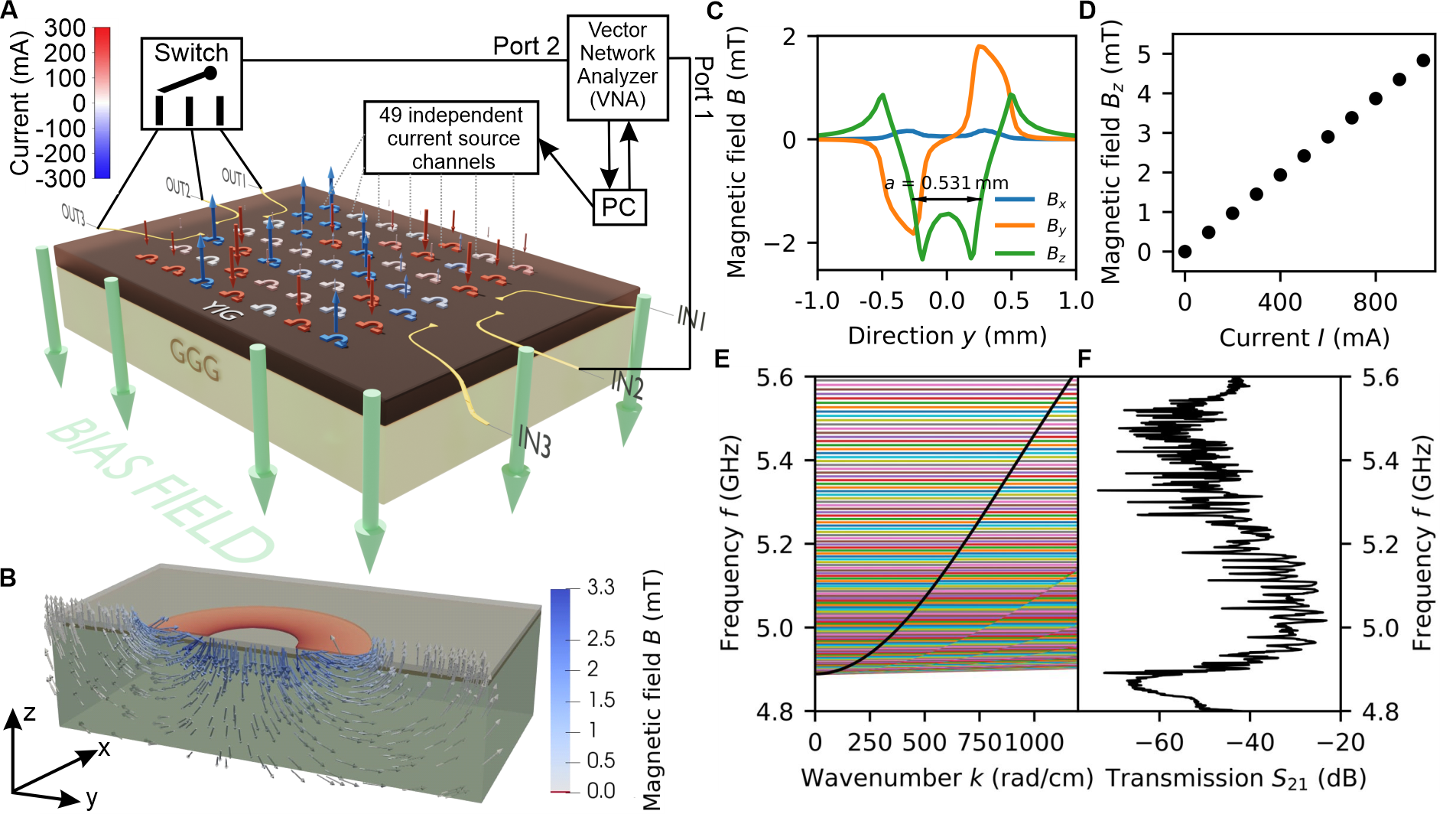
The processor’s propagating spin wave reference signal is plotted in Fig. 1F, taken at zero applied currents in the omega-shaped loops, transmission in dB versus frequency in GHz. We measure insertion losses (between VNA ports 1 and 2) of about 25 dB, which is related to the spin-wave loss during propagation over the distance of 2.2 cm and to the relatively low efficiency of spin-wave excitation and detection by the antennas (?). Another prominent feature of the spectrum involves dips where the propagation of spin waves is suppressed at particular frequencies. The formation of these dips is explained in the plot shown in Fig. 1E, which displays the analytically calculated spin-wave dispersion relations of the YIG film (?). The fundamental mode of the FVMSWs is the highest in energy (highlighted in bold in Fig. 1E). It is clearly evident how the fundamental mode of propagation aligns with the experimental transmission measurements regarding frequency range. The dispersion relation in Fig. 1E also shows the higher thickness mode or what is called Perpendicular Standing Spin Waves (PSSWs), and the hybridization of these modes with the fundamental mode resulting in the formation of the observed dips (?, ?). The frequency separation between the closest odd thickness modes where the dips are formed is about 4 MHz wide at the lower frequencies, approximately the same as the separation observed in the experiment. It is important to emphasize that these dips do not play any positive or negative role in the operation of the inverse design processor and are only artifacts associated with the concrete experimental configuration. However, from the analysis of the fundamental mode (bold) dispersion curve and its comparison to the transmission spectrum, we can deduce the wavelength working region by matching the highest frequency on the propagation spectrum to the right wavenumber 0.111 rad/m from the calculated dispersion and using the magnetostatic approximation as the lower limit where, 3.55 rad/cm, that corresponds to a working region of 56.6 m up to 17.7 mm.
The proposed design for the magnonic processor offers high tunability through its many degrees of freedom while supporting a stable operational range across a wide spectrum of frequencies and wavelengths. Thus, this processor concept serves as a versatile template for future magnonic devices that can accommodate 5G and future 6G technologies after miniaturization and conversion to a non-volatile operating state, as discussed below.
Inverse problem algorithms
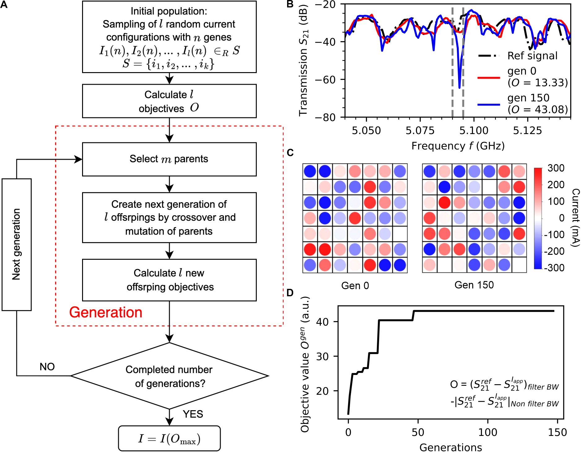
Two algorithms were used to test the performance of the inverse-design processor. The first is a genetic AI-driven algorithm representing a machine learning optimization process. It relies on creating a new generation by the crossover of the best-performing parents and introducing mutations – see Fig. 2A (?). The algorithm starts by creating a sample generation of random configurations with genes, is set to 49, corresponding to the 49 current values in the DC loops, and is assigned to the value of 50 in this concrete case, corresponding to the number of current loops. It provides the command for each current source channel to apply the corresponding current and then commands the VNA to measure spectra corresponding to the configurations. The transmission data is returned to the PC, and the optimizer calculates each configuration’s objective value . As a first example, we use this genetic algorithm to realize a notch filter functionality, where we only use one input and one output (between and ). The objective function of a notch filter is defined as follows:
,
where is the transmission parameter from port 1 port 2 when zero currents are applied to the DC loops, is the transmission parameter from port 1 port 2 when the currents of configuration are applied. To optimize the objective function, the losses within the filter bandwidth (BW) are maximized, while minimizing any changes occurring outside the filter bandwidth.
From the set of objectives calculated, the optimizer selects parents with the largest , where is set to 10, and uses them to create the next generation of offspring. It calculates the of each offspring from the new generation, and iterates until it has completed the number of generations commanded. The evolution of objective value as a function of generation number is plotted in Fig. 2D. An example of a 5 MHz BW notch filter that is realized using the genetic algorithm is shown in Fig. 2B. It compares the reference signal to the best offspring of generation 0 and the best in generation 150 for a notch filter with a center frequency of 5.0925 GHz. The figure illustrates the signal’s progression from generation 0 ( 13.33), where the maximum attenuation achieved is -8.3 dB at -26.57 dB compared to -34.89 dB. By generation 150 ( 43.08), the maximum attenuation occurred at -31.3 dB compared to -64.5 dB, resulting in -33.2 dB attenuation, solely attributed to the applied current determined by the algorithm. The current distribution in the omega-shaped loops is shown for both generation 0 and generation 150 in Fig. 2C with color coding in which red and blue correspond to opposite current polarities.
The genetic algorithm, leveraging its adaptability and robustness, consistently yields optimal solutions in our experiments, showcasing its effectiveness in optimizing and configuring complex systems.
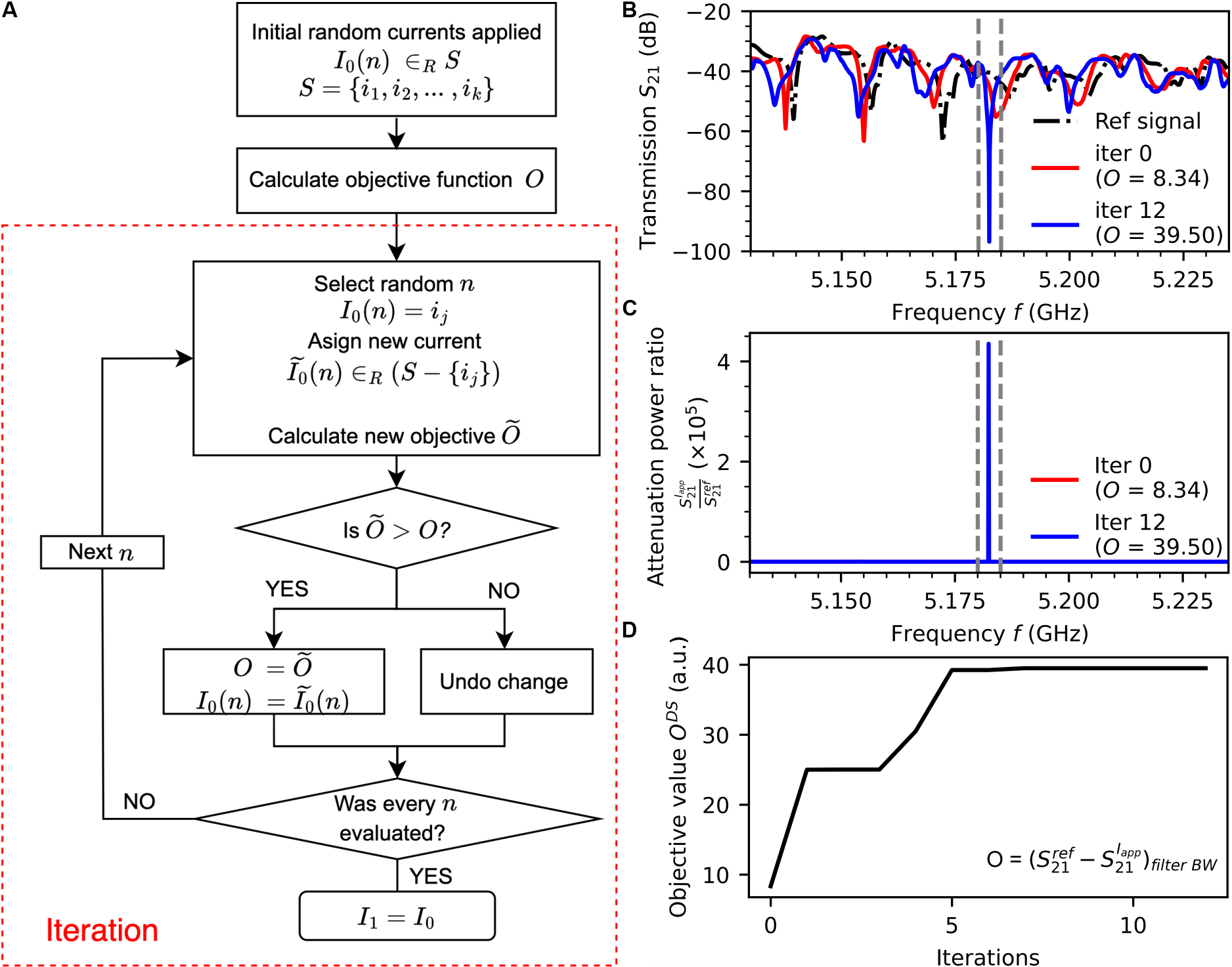
The second optimization algorithm that has demonstrated high performance in the developed inverse-design processor is a Direct Search (DS) algorithm, which is very similar in concept to Direct Binary Search (DBS) algorithms used in (?, ?). It relies on a set of finite values defined by the user instead of the binary approach to find the optimum solution. It begins by creating an initial random current configuration where is the variable that represents the number of the current loops in the array. The initial random configuration is a set of 49 current loops, each taking a random value from the set – see Fig. 3A. It calculates the objective function of the initial state and then chooses a random loop , checks its current value e.g. , and chooses another current value from the set . It calculates the new objective after the change, compares it to the original , and decides to keep the previous current value or apply the new one based on which results in the largest objective value . The optimizer continues over all 49 loops until each has been randomly changed once, one at a time. The first iteration is complete when it has gone over all the loops, progressing to the next state of . In Fig. 3B, the resulting notch filter functionality at a center frequency of 5.1825 GHz and a filter BW of 5 MHz using DS is shown together with the reference signal and iteration 0. The plot illustrates the signal progress within the rejection band, beginning at iteration 0 with an initial value of 8.34, corresponding to a maximum attenuation of -13.025 dB at -55.24 dB relative to -42.25 dB. By the final iteration ( 39.5), the attained attenuation reached -56.4 dB, corresponding to -96.83 dB compared to -40.45 dB. The evolution of objective value over the number of iterations is shown in Fig. 3D with the objective function defined as follows:
.
In this case, the objective values were calculated by considering only the filter BW and not any changes that occurred outside the filter region since the measured changes outside the filter BW were insignificant.
To focus on the effect induced solely by the reconfigurable medium, the attenuation power ratio was calculated as a function of frequency – see Fig. 3C. The attenuation power ratio is calculated as follows:
,
where is the difference between the transmission signal of iteration and the transmission of the reference signal at every frequency point. The attenuation power ratio introduced above and in Fig. 3C subtracts the reference signal from the final signal of the filter to show the induced attenuation by the reconfigurable medium. The figure shows a 10 attenuation in the filter BW while maintaining the changes minimal outside the filter region.
Contrary to the expectation of requiring a complex algorithm to configure more advanced functionalities, the straightforward and simplistic Direct Search algorithm (DS) exhibits remarkable promise in efficiently solving any inverse-design challenge with as little as 12 iterations in some cases.
Demonstrator 1: Notch filter
A notch filter is a device used abundantly in RF technologies to suppress undesirable signals at specific frequency ranges from the original signal, like noise. The filter uses one input and one output to perform the functionality. Figure 4A and 4B show 18 different 5 MHz BW notch filters realized at 0 dBm and 15 dBm input power, respectively. They were realized using the genetic algorithm process explained in Fig. 2A over a wide range of center frequencies. The performance of the notch filters is shown in terms of the attenuation power ratio, introduced in the previous section. The center frequencies considered were 30 MHz apart starting with center frequency 5.0925 GHz up to center frequency 5.3325 GHz, which covers a wavelength range of 70 m to 110 m.
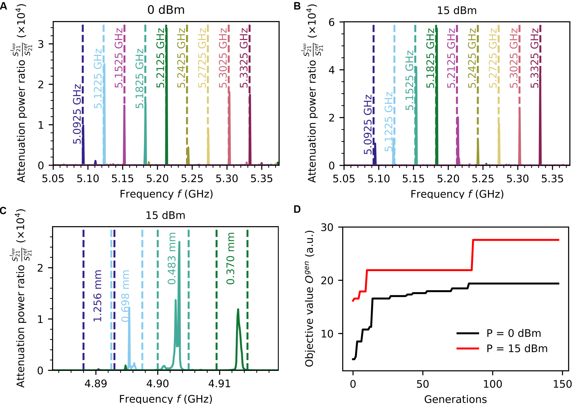
The average attenuation power ratio achieved is around 210 with the lowest notch filter attenuation (at center frequency 5.2425 GHz, and input power 0 dBm) 0.510 and highest attenuation (at center frequency 5.1825 GHz ,and input power 15 dBm) 5.910. Nevertheless, this frequency range only encompasses wavelengths significantly smaller than the magnetic field spatial distribution of about 0.53 mm – see Fig. 1C, and the spatial dimension of one loop of 1.1 mm. Figure 4C depicts the notch filters covering the lower range of at 15 dBm, representing wavelengths between 0.37 mm and 1.256 mm. The frequency steps are not kept linear in this limit, due to the non-linear dispersion behavior of the spin waves at this range. Instead, the step was kept constant with correspondence to the shorter wavelengths notch filters, at 40 rad/cm. It is important to note that the notch filter at the center frequencies 4.8906 GHz, with 1.256 mm, a wavelength larger than both the spatial dimension of the loop and its spatial field distribution, has achieved an attenuation power ratio of approximately 200. For each notch filter, a separate optimization procedure was performed at the defined center frequency using the same objective function shown in Fig. 2D.
A power study was conducted for one center frequency to compare the unit’s performance at these two regimes. The comparison was performed using the same random configurations. As seen in Fig. 4D, the objective value at 15 dBm of generation 0 was almost double of that at 0 dBm, meaning that the same current configuration resulted in larger attenuation in the BW by solely going into the weakly non-linear regime. The result of the power study was to be expected as the added scattering behavior of spin waves in the non-linear regime can aid in reaching higher suppression and finding the solution to the inverse-design problem at hand faster.
The main purpose of changing the center frequency of the rejection band is to validate the ability of the inverse-design processor to solve the inverse problem for wavelengths in a wide range. To avoid the unfortunate situation that the filter works for a single concrete (resonance) wavelength, given, e.g., by the characteristic dimension of one current loop or by the spatial distance between them.
Thus, our investigations have shown that this is not the case, and the developed processor can indeed solve the task for any accessible wavelength in the experimental setup. On the other hand, our studies have shown that the inverse problem can be solved when the wavelength (about 1.3 mm) is larger than the effective spatial dimensions of an inhomogeneity (about 0.5 mm). However, the efficiency drops significantly, and the preferred operating regime for such a processor is when the wavelength is smaller or much smaller than the characteristic size of a medium non-uniformity.
Demonstrator 2: Two-port magnonic frequency demultiplexer
A two-port frequency demultiplexer utilizes one input antenna and two output and antennas. It was realized by defining two 5 MHz frequency ranges, with center frequencies 5.1525 GHz and 5.1825 GHz. The two frequency ranges are excited at , and the optimization algorithm is used to find the optimum current configuration to separate and at the two different outputs. The optimization process used to achieve this two-port frequency demultiplexer is the Direct Search (DS) shown in Fig. 3A. The objective function was defined as the multiplication of the two output signals as follows:
.
The objective function achieves optimization when it is maximized. It is designed to attenuate at and at , effectively routing to and to . The states where both components, & , exhibit evolution in the opposite direction (when both yield negative values) are taken into account and disregarded. Figure 5A shows the transmission signal as a function of frequency, where VNA port 1 is connected to the input side of the processor, and port 2 is connected to the mechanical switch that connects to and .
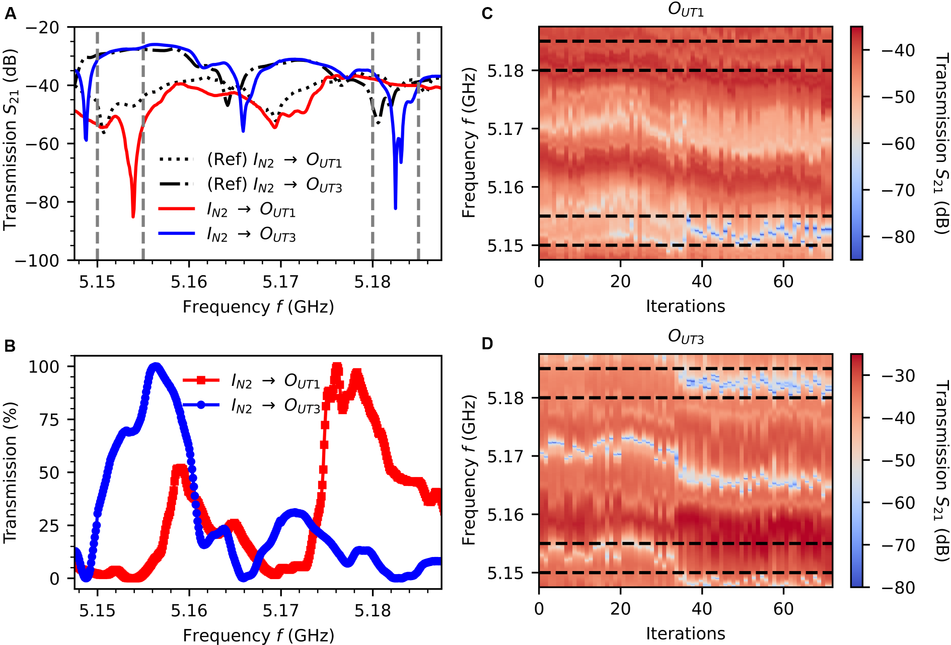
The measurement process begins by obtaining a reference transmission signal (with zero currents applied) at . Subsequently, the VNA port 2 is directed to through the mechanical switch, and the corresponding reference signal is recorded. These reference signals serve as the basis for calculating all objective values once the current configurations instructed by the optimizer begin to be applied. The figure displays two reference signals corresponding to the two outputs, along with the demultiplexer’s signal after the completion of the optimization process. The optimization process has successfully attenuated the transmission of and ranges at and , respectively, per the defined objective. Simultaneously, it has maintained the transmission at the same level as their respective reference signals at the defined outputs ( to and to ). The normalized transmission percentage shown in Fig. 5B, clearly illustrates the extended attenuation window compared to the defined frequency ranges, approximately double the defined windows. This highlights the robustness of the demultiplexer. The 100% transmission is a relative value of each independent output to itself. Figure 5C and 5D show the color map of the transmission in dB when considering the frequency and the number of iterations for and , respectively. The plots show the evolution of the attenuated signal in the defined frequency ranges (marked with grey dashed lines) of each output through the number of iterations. The emergence of distinct rejection bands for the two different outputs becomes evident after approximately 35 iterations, as indicated by the formation of blue regions (-85 dB for and -80 dB for ) within the specified attenuation frequency ranges. Conversely, those frequency ranges appear red when considering the opposing output, indicating high transmission.
III Discussion
Our magnonic processor offers an excellent platform for demonstrating experimental inverse-design solving on a proof-of-concept basis. It offers further testing and development of AI-driven optimization algorithms that can be used for inverse-design tasks in 5G and 6G RF applications, among others. To advance the concept of having a reconfigurable processor even further – binary logic gates or neuromorphic data processing units, our device can be used to understand and fully control spin-wave non-linearity and use it in creating more complex functionalities. As it has been shown in photonics (?, ?), the wave non-linearity, namely the ability of the wave to change the media and, consequently, its dispersion relation, by the increase in the wave amplitude, is important in inverse-design solving and significantly enhances the performance of the inverse-design optimizers. Spin waves are rich in versatile nonlinear phenomena inherent to their nature, eliminating the necessity for specialized nonlinear media. Roughly, one can split the phenomena into two types (?): controllable, which only slightly shifts the spin-wave dispersion curve inducing a phase accumulation of the wave (?, ?) as well as stochastic like 3-magnon (?) and four-magnon scattering (?). The stochastic processes are not desirable for the deterministic inverse-design approach, and the application of very large powers to the antennas deteriorates the operational characteristics of the devices, as has been shown in (?). In this work, we tested the two regimes at a power of 0 dBm and 15 dBm. In the linear regime, the spin-wave amplitude variation occurring by forming a complex interference pattern is not significant enough to change the media; the spin waves have the same dispersion in all spatial points of the processor working region. The system remains within the weakly nonlinear regime in the second scenario, where the input power is 15 dBm. While the dispersion remains unchanged, modifications occur in regions characterized by high spin-wave pattern accumulation. As a result, the spin-wave amplitude becomes significantly larger. Within these regions, the nonlinear characteristics of spin-waves lead to a reduction in the effective magnetization of YIG (?, ?). Consequently, this shifts their dispersion toward higher frequencies and alters the spin-wave wavelength and group velocity within this region. The frequency of FVMSW in the small approximation ( 0) is defined as , whereas in the large approximation (), it is defined as (?). We have observed that the inverse-design processor at 15 dBm successfully resolved the problem with approximately double the objective value , resulting in -87 dB attenuation in the filter BW compared to about -62 dB total attenuation at 0 dBm, starting with the same random sampling of the genetic algorithm. Furthermore, Fig. 4D clearly shows that the target values are higher for the weakly nonlinear regime for all generations.
If we analyze the speed with which the device can be reconfigured, in our concrete case, it was given by the speed of the current sources and their control by the PC, and it is in the range of hundreds of microseconds. We did not define the goal of fast reconfiguration, as we were focused on testing and realizing the concept of reconfigurable inverse-design magnonics. But the fundamental limitation, in this case, would be the inductance associated with the current loops, and a good reference to the limiting speed is the dynamic magnonic crystal studied in (?, ?). There, they used a high inductance meander and realized the on/off of the field within about 5 ns. This switching time was also defined by the power source rather than the device. Thus, we can claim that the reconfigurability of the developed processor within a one-nanosecond timeframe is feasible, with its implementation being merely a technical matter. Consequently, it possesses the capability to effectively address the inverse problem in real time.
From an applied point of view, we do not consider the processor as a device that can compete with the surface acoustic wave (SAW) or bulk acoustic wave (BAW) microwave passive components such as filters and multiplexers currently used in mobile phones and other communication systems, but rather as a platform to study the performance and potential of the inverse design for 5G RF applications. For a real device, the miniaturization of the processor is required both in the magnonic media (e.g. today we work with magnonic waveguides of 50 nm width (?)) as well as in the effective size of the introduced inhomogeneities. Moreover, the proposed proof-of-concept demonstrator uses considerable electrical currents and is energetically inefficient. Therefore, the formation of field inhomogeneities should be realized by other non-volatile methods well studied in the field of magnonics (?, ?). The current loops could potentially be replaced by an array of individually-controlled nanomagnets of a complex shape to achieve multiple degrees of freedom (simple-shaped nanomagnets were already used in (?, ?, ?)). In this way, the RF device would consume energy only at the moment of reconfigurability of its operational parameters while remaining a passive device during operation.
IV Conclusions
We have developed a highly reconfigurable magnonic processor with a high degree of tunability, currently exploiting 10 of the 10 available degrees of freedom. Through our work, we have demonstrated the processor’s capabilities by realizing RF filter and demultiplexer functionalities. These devices’ implementation relied on employing AI-driven optimization algorithms to solve the inverse-design tasks. Our filter function achieved significant attenuation in the rejection band, reaching approximately 410. Similarly, the demultiplexer function exhibits a high attenuation of approximately -40 dB within the defined frequency ranges for the corresponding outputs. The proposed magnonic media can potentially be reconfigured on the time scale of a nanosecond. With its intricately designed reconfigurable region, we are confident that our processor can achieve various other functionalities for RF applications for 5G and 6G, logic gates, or neuromorphic computing.
Acknowledgments
The financial support by the Austrian Science Fund (FWF) via Grant No. I 4917-N (MagFunc) is acknowledged. A.C. acknowledges the financial support by the European Research Council (ERC) Proof of Concept Grant 101082020 5G-Spin. S.K. acknowledges the support by the H2020-MSCA-IF under Grant No. 101025758 (”OMNI”). Q.W. acknowledges the support from the National Key Research and Development Program of China (Grant No. 2023YFA1406600). We are grateful to Prof. Dr. D. Bozhko for his kind support in calculating the spin-wave dispersion curves in YIG film and to Prof. P. Pirro and Prof. G. Csaba for valuable discussions on the magnonic processor concept. We acknowledge the efforts of ElbaTech Srl in the development of the custom-made multichannel current sources.
References
- 1. H. Wang, et al., Nature 620, 47 (2023).
- 2. D. McDuff, et al., Towards Accurate Differential Diagnosis with Large Language Models (2023).
- 3. A. Kumar, S. Tripathi, K. Rao, Machine learning techniques for VLSI chip design (2024).
- 4. A. Y. Piggott, et al., Nature Photonics 9, 374 (2015).
- 5. B. Gholipour, et al., Advanced Optical Materials 3, 635 (2015).
- 6. A. N. Tait, et al., Physical Review Applied 11, 064043 (2019).
- 7. T. Wu, M. Menarini, Z. Gao, L. Feng, Nature Photonics 17, 710 (2023).
- 8. R. Bruck, et al., Optica 3, 396 (2016).
- 9. J. Cheng, et al., ACS Photonics 10, 2173 (2023).
- 10. A. Barman, et al., Journal of Physics: Condensed Matter 33, 413001 (2021).
- 11. A. V. Chumak, et al., IEEE Transactions on Magnetics 58, 1 (2022).
- 12. V V Kruglyak, S O Demokritov, D Grundler, Journal of Physics D: Applied Physics 43, 260301 (2010).
- 13. Q. Wang, A. V. Chumak, P. Pirro, Nature Communications 12, 2636 (2021).
- 14. M. Kiechle, et al., IEEE Magnetics Letters 13, 1 (2022).
- 15. A. Papp, W. Porod, G. Csaba, Nature Communications 12, 6422 (2021).
- 16. A. V. Chumak, et al., Nature Communications 1, 141 (2010).
- 17. Y. Wu, et al., Advanced Materials 29, 1603031 (2017).
- 18. C. Dubs, et al., Journal of Physics D: Applied Physics 50, 204005 (2017).
- 19. A. A. Serga, A. V. Chumak, B. Hillebrands, Journal of Physics D: Applied Physics 43, 264002 (2010).
- 20. A. G. Gurevich, G. A. Melkov, Magnetization Oscillations and Waves (1996).
- 21. C. Abert, L. Exl, F. Bruckner, A. Drews, D. Suess, Journal of Magnetism and Magnetic Materials 345, 29 (2013).
- 22. C. Abert, The European Physical Journal B 92, 120 (2019).
- 23. T. Schrefl, et al., Numerical Methods in Micromagnetics (Finite Element Method) (2007).
- 24. Q. Wang, et al., Nature Electronics 3, 765 (2020).
- 25. D. A. Connelly, et al., Scientific Reports 11, 18378 (2021).
- 26. D. A. Bozhko, et al., Physical Review Research 2, 023324 (2020).
- 27. B. A. Kalinikos, A. N. Slavin, Journal of Physics C: Solid State Physics 19, 7013 (1986).
- 28. A. A. Serga, et al., Physical Review Letters 99, 227202 (2007).
- 29. A. F. Gad, Multimedia Tools and Applications (2023).
- 30. B. Shen, P. Wang, R. Polson, R. Menon, Nature Photonics 9, 378 (2015).
- 31. S. Molesky, et al., Nature Photonics 12, 659 (2018).
- 32. T. Hughes, M. Minkov, I. Williamson, S. Fan, ACS Photonics 5, 4781 (2018).
- 33. Q. Wang, et al., Science Advances 4, e1701517 (2018).
- 34. X. Ge, R. Verba, P. Pirro, A. V. Chumak, Q. Wang, Nanoscaled magnon transistor based on stimulated three-magnon splitting (2023).
- 35. A. V. Chumak, A. A. Serga, B. Hillebrands, Nature Communications 5, 4700 (2014).
- 36. Q. Wang, et al., Science Advances 9, eadg4609 (2023).
- 37. A. V. Chumak, T. Neumann, A. A. Serga, B. Hillebrands, M. P. Kostylev, Journal of Physics D: Applied Physics 42, 205005 (2009).
- 38. B. Heinz, et al., Nano Letters 20, 4220 (2020).
- 39. A. Imre, et al., Science 311, 205 (2006).
- 40. F. Kronast, et al., Nano Letters 11, 1710 (2011).
- 41. A. Haldar, D. Kumar, A. O. Adeyeye, Nature Nanotechnology 11, 437 (2016).