Spin-orbit proximity in MoS2/bilayer graphene heterostructures
Abstract
Van der Waals heterostructures provide a versatile platform for tailoring electronic properties through the integration of two-dimensional materials. Among these combinations, the interaction between bilayer graphene and transition metal dichalcogenides (TMDs) stands out due to its potential for inducing spin-orbit coupling (SOC) in graphene. Future devices concepts require the understanding the precise nature of SOC in TMD/bilayer graphene heterostructures and its influence on electronic transport phenomena. Here, we experimentally confirm the presence of two distinct types of spin-orbit coupling (SOC), Ising () and Rashba (), in bilayer graphene when interfaced with molybdenum disulphide, recognized as one of the most stable TMDs. Furthermore, we reveal a non-monotonic trend in conductivity with respect to the electric displacement field at charge neutrality. This phenomenon is ascribed to the existence of single-particle gaps induced by the Ising SOC, which can be closed by a critical displacement field. Remarkably, our findings also unveil sharp peaks in the magnetoconductivity around the critical displacement field, challenging existing theoretical models.
I Introduction
Spin is emerging as a promising alternative or complement to charge for information storage and processing [1]. Spin-orbit coupling (SOC) is crucial in spin-based devices, enabling manipulation of spin states through time-dependent electric fields [2, 3]. Bernal bilayer graphene (BLG) holds potential for spintronics [4] and quantum computing [5], with recent studies indicating long spin relaxation times in BLG quantum dots [6, 7, 8]. However, intrinsic Kane-Mele (KM) SOC [9] in graphene is weak () [10, 11]. Various methods have been explored to enhance SOC in BLG, including interfacing with high-SOC substrates. Transition metal dichalcogenides (TMDs) have shown promise in this regard, offering significant SOC enhancements (from ) without compromising graphene’s electronic quality [12, 13, 14]. Additionally, the combination of BLG on WSe2 has recently shown to host an unexpected superconducting phase, where the SOC seems to play a major role [15, 16], prompting further study of such heterostructures.
The extrinsic SOC induced in BLG by the TMDs is described by the Hamiltonian [17]
| (1) |
where represents the valley index, denote spin Pauli matrices, and are Pauli and unit matrices operating on the sublattice degree of freedom within the layer in contact with the TMD [see schematic in Fig. 2(e)]. The first term, known as the Ising SOC, acts similar to an effective out-of-plane magnetic field with a valley-dependent sign. It lifts the four-fold spin and valley degeneracy at the points, forming spin-valley locked Kramers doublets. The second term is a Rashba type of SOC [18], favoring an in-plane spin polarization perpendicular to the sublattice isospin vector.
Intensive theoretical [17, 19, 20, 21, 22, 23] and experimental efforts [12, 13, 24, 25, 26, 14, 27] in understanding and quantifying SOC proximity effects, have led to a range of values for the relative strength of the two SOC terms depending on analysis method. This is because the strength of SOC is often inferred indirectly, for example, through the extraction of relaxation times obtained from quantum interference effects such as weak antilocalization (WAL) [28, 29, 30]. In contrast, the fundamental frequency of the Shubnikov-de Haas oscillations (SdHOs) offers a direct measurement of the Fermi surface and is suitable for determining the band splitting induced by SOC [31]. However, the energy resolution of this technique is limited by the broadening of the Landau levels, necessitating high electron mobilities and low disorder potentials.
Here, we conduct magnetotransport experiments on a dual-gated MoS2/BLG heterostructure. First, we analyze SdHOs to quantify proximity-induced SOC. Our results confirm the presence of both Ising () and Rashba () SOC. Despite their comparable strength, we show that the splitting of the low energy bands mainly arises from the Ising SOC. Additionally, we observe a non-monotonic conductivity response to an applied displacement field when BLG is charge neutral. Our tight-binding calculations show how the displacement field opposes the Ising SOC, closing single-particle gaps in the spin-polarized bands at a critical value and causing local maxima in the conductivity. At this critical field, the application of an external magnetic field rapidly suppresses the conductivity, challenging existing theoretical models and suggesting the involvement of many-body interactions.
II Proximity induced spin-orbit coupling
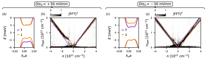
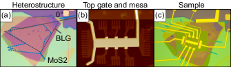
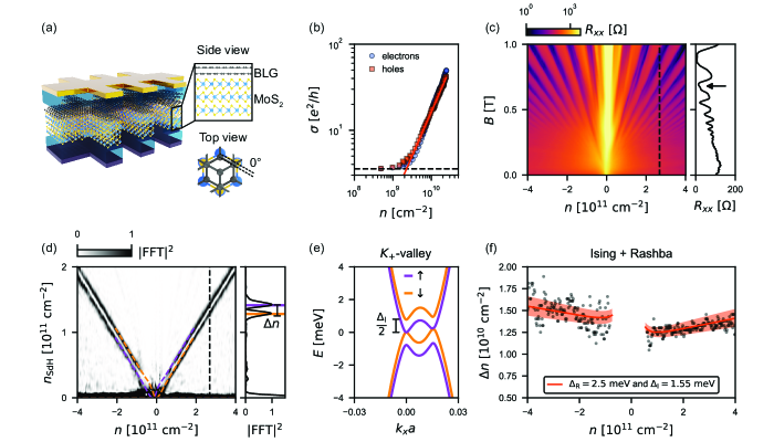
Determining the SOC gap in BLG via magnetotransport experiments is challenging due to disorder-induced density fluctuations . Shown in Figure 1(a) is the schematic of our sample, comprising BLG atop three layers of MoS2, encapsulated within hexagonal boron nitride (hBN), and placed on a graphite bottom gate. The use of hBN dielectrics and a graphite layer minimizes density fluctuations [32], evident from the low density at which conductivity saturates in our sample [Figure 1(b)]. High charge carrier mobilities [ at , see Supplementary Information] indicate minimal impact of the MoS2 layer on BLG’s electronic properties compared to hBN-encapsulated Bernal BLG devices [33].
We analyze SdHOs at zero displacement field () and low magnetic fields () to determine the band splitting induced by the SOC. Figure 1(c) shows the longitudinal resistance as a function of and electron density at . Pronounced minima in resistance occur at filling factors ( an integer), characteristic of pristine BLG. In addition, small oscillation maxima appear in the SdH minima (highlighted by the arrow in the right panel), suggesting the presence of a broken symmetry.
To determine the oscillation frequency of the SdHOs, we employ a numerical fast Fourier transform (FFT) of calculated line-by-line for each density, as shown in Fig. 1(d). The FFT reveals two clear frequencies and , resulting from the splitting of the Fermi surface, which is attributed to the influence of the MoS2 substrate through the spin-orbit proximity effect. The sum of the electron densities () obtained from the SdHO matches the Hall density by accounting for the twofold valley degeneracy, as expected.
The two SOC terms in equation (1) yield distinct density dependencies for the spin-orbit splitting. The Ising SOC induces a constant splitting as a function of the Fermi energy (and hence density), while the Rashba term leads to a splitting that increases with the Fermi energy. Although the splitting in Fig.1(d) initially appears constant with carrier density, a closer examination of in Fig.1(f) reveals a small but detectable slope. By aligning the density difference obtained from the tight-binding model (see Methods .4 and .5) with the data (illustrated by the red solid line), we find and \bibnoteWe acknowledge that the numerical outcome of the fit can be subtly influenced by the choice of the tight-binding intralayer and interlayer coupling parameters of BLG, referred to as the Slonczewski–Weiss–McClure parameters ( and ). These parameters dictate the curvature of the bands, thereby affecting the conversion between energy and density, as elaborated in detail in Methods .5. In addition, we chose to neglect the parameter , which governs the particle-hole asymmetry. This decision was made because including would introduce an offset between the electron and hole doping that is not observed in our experiments.. Despite the similar magnitudes of the two SOC terms, the weak density dependence exhibited by suggests that the primary contribution to the splitting of low-energy states stems from the Ising SOC (see also discussion in Supplementary Information). The theoretically predicted densities with these parameters are overlaid against the total density in Fig. 1(d) as orange and violet dashed lines, demonstrating good agreement with the experimental data.
We validate our findings at finite displacement fields, leveraging the layer-dependent SOC induced by the asymmetric structure of our sample [3]. This layer selectivity is demonstrated in Extended Data Fig.I, where the electron wave function is polarized via the applied displacement field in one layer or the other, depending on its sign. A detailed discussion of these data can be found in the Supplementary Information.
Next we continue the discussion by investigating the impact of SOC on the electrical conductivity () of BLG at charge neutrality (CN).
III Conductivity at charge neutrality
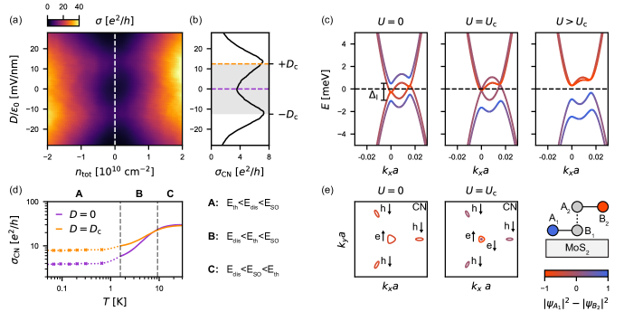
Measurements of reveals a non-monotonic dependence on the displacement field [Fig. 2(a)], which appears in a narrow density range () around CN. A local minimum at is surrounded by conductivity maxima at , as highlighted in the line cut at presented in Fig. 2(b).
This dependence can be understood by taking into account the influence of SOC on the BLG band structure. From tight-binding calculations we find that the Rashba SOC has little effect on the low energy bands (see Supplementary Information for more details). For this reason, we consider only the Ising SOC in the following discussion. The outcome of the band structure calculations is presented in Fig. 2(c), shown for the -valley and three characteristic interlayer potential energies (). First, we consider the case in the left panel. We observe that the band structure comprises two pairs of bands, one split by the energy and partially layer-polarized on the bottom layer (blue), while the other pair is degenerate at two points along and is partially polarized on the top layer (red). Due to their partial layer polarization, the application of a displacement field shifts the two pairs of bands relative to each other based on their layer polarization. Notably, the calculations show that a band gap emerges only once the interlayer potential energy exceeds the critical value (right panel), i.e. once counteracts the SOC, resulting in the closure of the gap between bands with the same spin [see Fig.2(e) for the spin texture] \bibnote A recent experiment by Seiler et al. [56] in high-quality BLG demonstrated that trigonal warping causes the overlap (approximately ) of conduction and valence bands, resulting in a semi-metallic phase. Due to the band overlap, a finite displacement field is necessary to suppress the density of states at charge neutrality (CN) and open the band gap. However, this effect does not lead to a non-monotonic dependence of the conductivity, as observed in our experiment.. This elucidates why in the experiment, the conductivity starts decreasing with increasing displacement fields only when , and associate the maxima in the conductivity with the closure of the SOC gaps. We verify this interpretation by converting into a displacement field, taking into account interlayer screening (see Methods .6 for details). The conversion yields a displacement field of , in good agreement with the experimental value of . Furthermore, the local conductivity minimum at is observed only at low density and vanishes around , which corresponds to the density required to fill the spin-orbit splitting of the bands, as demonstrated in Fig. 1(f).
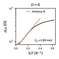
The local minimum in conductivity at prompts consideration of a potentially insulating phase arising from the presence of a gap, as reported for BLG fully encapsulated in TMDs [14]. To verify this, we examine the temperature dependence of the conductivity in Fig.2(d). Over the temperature range of , the conductivity increases by one order of magnitude, indicative of insulating behavior. However, the data only conforms to the Arrhenius law within a very limited temperature range (shown in Extended Data Fig.II) and saturates to rather large conductivity values at low temperatures. Similarly, the conductivity at the critical field also increases with temperature. Thus, although the insulating behavior is affected by the applied displacement field, it is consistently observed across all displacement fields at CN.
To further understand the temperature dependence, we compare the thermal energy with the other characteristic energy scales determined by disorder () and SOC (). First, we take into account the disorder potential, which induces density fluctuations of the order . These fluctuations are converted into an energy scale using an effective mass approximation (, where is the bare electron mass [36]) and taking into account the twofold valley degeneracy. At low temperatures (), the conductivity is governed by disorder-induced electron-hole puddles, causing the saturation of the conductivity in the temperature range labeled A in Fig. 2(d). Second, the SOC introduces gaps between bands of the same spin at , as illustrated in Fig.1(c). The presence of these “spin-resolved” gaps, even without a real band gap, could explain the insulating behavior of the conductivity. Effectively, if spin is conserved in thermal activation processes, carriers cannot be thermally excited from the highest occupied valence band into the lowest unoccupied conduction band, because these bands have opposite spin. Therefore, carriers thermally excited above the spin gap should result in an increase of conductivity with increasing temperature, which is precisely happening in the temperature range labeled B in Fig. 2(d). In regime C (), the thermal energy surpasses the SOC gap, causing the conductivity to saturate again.
Based on the results presented above, we attribute the dependence of conductivity on displacement field, density and temperature to the presence of spin-orbit-induced gaps in the spin-polarized bands in the absence of a global band gap.
IV phase diagram
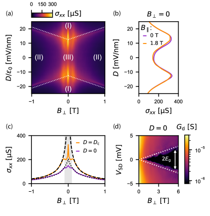
In the final section of this work, we describe magnetotransport measurements at CN. Figure 3(a) illustrates the longitudinal conductivity as a function of out-of-plane magnetic field () and displacement field at a temperature of . With the exception of the low magnetic field peaks at , which we discuss below, the phase diagram depicted in Fig. 3(a) bears resemblance to that of pristine BLG [39, 40]. Drawing on previous studies [41, 39], we partition the parameter space into three distinct regions.
Phases (I) and (II), occurring at large displacement and magnetic fields respectively, are anticipated to mirror the behavior of the BLG system in the absence of SOC. This is attributed to the dominance of energy scales dictated by the externally applied parameters ( and ) over the SOC gap . Hence, we attribute phase (I) to the layer-polarized insulating state arising from the band gap induced by the displacement field, as illustrated in Fig. 2(c). Phase (II) represents the insulating state of the quantum Hall state. In this phase, our bias spectroscopy measurements uncover the presence a gap [Fig.3(d)], which qualitatively explains the observed suppression of the conductivity [see dotted and dashed lines in Fig.3(c)]. This behavior aligns with the canted antiferromagnetic phase observed in pristine BLG [42]. Moreover, the boundaries between Phase (I) and (II) (indicated by white dotted lines and elaborated in detail in Supplementary Information) exhibit common characteristics with those observed in pristine BLG: the insulator-insulator transition features enhanced conductance [41, 38], and the displacement field required to induce the transition is [39, 43, 44, 42]. On the other hand, Phase (III), emerging at and , is expected to differ from BLG samples not in proximity with a TMD layer. Single-particle band structure calculations reveal that this phase is characterized by spin-polarized bands [Fig. 1(e)] with partially layer-polarized wave functions [left panel in Fig. 2(c)]. As we have discussed in Sec.III, this phase shows thermal activation due to the presence of spin-orbit gaps in the spin-polarized bands without the presence of a global band gap, as illustrated by Fig. 3(d). While the magnetic field induces a gap in the spectrum, no distinct phase transition is observed between Phase (III) and Phase (II). This is likely due to both phases being overall layer unpolarized when considering the occupied valence bands, as demonstrated by the phase transition induced by the displacement field.
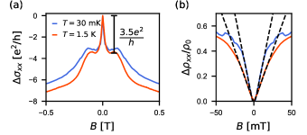
Now, we examine the sharp magnetoconductivity peaks at [see orange curve in Fig. 3(c)], a novel feature of spin-orbit proximitized BLG not previously reported. With current theoretical models unable to fully explain these peaks, we explore various possibilities.
At first glance, the sharp peak in the orange curve in Fig.3(c) resembles the signature of WAL, expected in materials with strong SOC. This effect has been observed in numerous transport experiments in SOC-proximitized graphene [28, 45, 25, 29, 13, 46, 47]. However, with a mean-free-path exceeding at finite density, the condition (where and represent the phase-coherence length and mean-free-path, respectively) required to observe this effect would never be fulfilled ( if fitting the peak with a WAL model, as detailed in the Supplementary Information). Furthermore, the magnitude of the peak () exceeds what would be expected for WAL, which typically reaches up to per conducting channel. Additionally, quantum interference effects are typically suppressed with increasing temperature due to the decrease in . In contrast, the magnitude of the peak in remains robust against temperature changes [see Fig.III in Extended Data]. For these reasons, we conclude that the peaks cannot arise from WAL.
Typically, distinguishing between how a magnetic field affects orbital or spin degrees of freedom involves tilting the field with respect to the plane. Orbital effects couple exclusively to , while spin couples to . In fig.3(b), we compare the conductivity at for and (the maximum available in our system), where no significant effect is observed on . The lack of an in-plane magnetic field dependence is consistent with the presence of Ising SOC, which is expected to align spins out-of-plane. Therefore, for an in-plane magnetic field dependence in conductivity to occur, the Zeeman energy would need to become comparable to the spin-orbit gap , estimated to occur at . In our experiments, the conductivity drops by nearly a factor of 2 at . This magnetic field corresponds to a Zeeman energy of only , much smaller than disorder. Therefore, it is unlikely that the Zeeman effect could be responsible for the observed magnetoconductivity peaks.
V Discussion
In this study we demonstrated that two type of SOC are present in spin-orbit proximitized BLG. Despite the similar magnitudes of the two SOC terms, the band splitting at zero displacement field shows little dependence on the total density, indicating that the Ising SOC predominantly influences the splitting within the density range under investigation. Our results align with previous observations of Ising superconductivity in WSe2/BLG heterostructures [16, 15], suggesting the potential for similar phenomena to occur in MoS2/BLG systems.
Furthermore, we observed an insulating phase at , leading to a non-monotonic electrical conductivity with respect to the displacement field. Insulating phases with a similar displacement field dependence have been also observed in charge neutral suspended BLG [41], albeit with an intrinsic SOC two orders of magnitude weaker than in our sample [9, 48]. While suspended BLG exhibits a gap at and [49], attributed to many-body correlations, our sample does not show this behavior [Fig.3(d)], suggesting a different underlying mechanism. The absence of such correlated phases in hBN-encapsulated Bernal BLG suggests that dielectric and gate screening effects may reduce the relevance of correlation phenomena. Thus, we conclude that SOC plays a crucial role in the emergence of the observed insulating phase at . This assertion aligns with findings by Island et al. [14], who reported a comparable insulating phase in BLG fully encapsulated in WSe2. While their explanation relied on SOC-driven band inversion, our observations suggest an alternative explanation, specifically single-particle SOC-induced gaps in spin-polarized bands in the absence of a global band gap [Fig.1(e)]. Our conclusion is supported by a detailed analysis of the SOC strength, a comparison between the band structure calculations and the displacement field dependence, as well as temperature dependent measurements.
While the zero magnetic field data are understood in terms of single-particle physics, we could not find a suitable theoretical model to describe the data at finite magnetic field. We speculate that the non-monotonic magnetic field dependence of at originates from many-body effects at CN. Electron interactions, particularly strong near CN due to the lack of screening, were predicted to drive an instability towards an ‘excitonic insulator’ phase, where carriers in valleys and exhibit strong particle-hole correlations [50, 51, 52, 53]. Previous measurements, while showing promising results regarding gap opening at CN, were inconclusive. This could be due to, among other reasons, a reduction in exchange interactions in the valley sector in the presence of spin degeneracy. In our system, with spin degrees of freedom polarized by SOC, carrier exchange responsible for the many-body physics at CN is expected to intensify. If this interpretation holds true, the system described here could serve as a platform to explore various intriguing effects anticipated for excitonic phases, such as vortices, merons, and the Josephson effect for charge-neutral particles.
Note from the authors. While preparing our manuscript, we became aware of a related study by A. Seiler at al., who investigated the interplay between SOC and Coulomb interaction in WSe2/BLG heterostructures, drawing conclusions on the phase diagram of SOC-proximitized BLG. It is remarkable that very similar data was obtained by two different groups, using a different TMD on bilayer graphene (MoS2 by our research group and WSe2 by Seiler et al.).
Methods
.1 Sample fabrication
We initiate the fabrication of our devices by assembling the heterostructure using a polymer-based dry transfer technique. Each layer is obtained through mechanical exfoliation of bulk crystals onto silicon/silicon dioxide wafers. The heterostructure comprises, from top to bottom, hBN, bilayer graphene (BLG), three layers of MoS2, hBN, and graphite. The finalized heterostructure is depicted in Extended Data Fig.IV(a).
The relative alignment of BLG with the MoS2 layer is known to influence the strength of the SOC [21, 20]. While the maximum induced SOC is anticipated around , the SOC is most stable against small uncontrolled twist angle variations at , ensuring better reproducibility. Therefore, during the fabrication process, we carefully align the edges of the MoS2 and BLG flakes, resulting in potential relative alignments of or . At , the SOC proximity is expected to vanish, leading us to conclude that the relative angle in our sample is .
Subsequently, the sample undergoes annealing in a hydro-argon atmosphere (H2/Ar: 5%/95%) at for 4 hours to remove polymer residues and enhance adhesion between the layers. The metallic top gate is defined using standard electron-beam lithography, followed by electron-beam evaporation (chromium/gold) and lift-off processes. The mesa is dry-etched using a reactive ion etching process with a CHF3:O2 mixture (40:4). An atomic force microscope image of the sample post-gate deposition and mesa etch is depicted in Extended Data Fig.IV(b).
In the final fabrication step, metallic edge contacts are deposited using electron-beam lithography, followed by electron-beam evaporation (chromium/gold) and lift-off processes. After resist development, we clean the contact area using an O2 reactive ion etching process before metal deposition. This ensures the resulting contacts are ohmic and low resistive (). An optical image of the sample at the conclusion of the fabrication process is presented in Extended Data Fig.IV(c).
.2 Dual-gated device
We employ a dual gate structure that allows for independent tuning of the charge carrier densities and displacement field . The density is defined as
| (2) |
and the displacement field is defined as
| (3) |
where and are the capacitance per area of the bottom and top gate, and are the voltages applied to the bottom and top gate. Additionally, and are offsets in the density and displacement field, respectively. These offsets are taken into account to compensate the asymmetries arising from factors such as the contact potential difference between hBN and MoS2 [17].
.3 Measurements
The measurements were performed in a pumped Helium-4 cryostat (for the temperatures above ) or in a dilution refrigerator with base temperature (estimated electronic temperature ).
The four-terminal resistance was measured with constant input current, by using a series resistor of or , depending on the resistance of the sample. The input voltage was generated at a frequency of roughly with a Lock-in amplifier. The current amplitude ranged from .
The bias spectroscopy measurements were done in a two terminal setup, where a DC voltage source was employed to generate the source-drain bias and a home-made voltage-to-current converter was used to detect the source-drain current.
.4 Tight-binding model
To determine the band structure we employ a four-band effective tight-binding model for BLG in the basis , where are the two atoms in the unit cell of a single graphene layer and their index represent the layer number [36]:
| (4) |
where , , is the inter-layer potential energy difference, is an energy difference between dimer and non-dimer atoms, and . The parameters are the Slonczewski–Weiss–McClure (SWM) parameters given in Tab. Tab.1.
| SWM parameters | |||||
|---|---|---|---|---|---|
| Exp. [54] | 3.0 | 0.40 | 0.3 | 0.15 | 0.018 |
| Th. [55] | 2.61 | 0.361 | 0.283 | 0.138 | 0.015 |
We include the extrinsic SOC given by equation (1). The SOC lifts the spin degeneracy but does not mix states from different -valleys. Therefore, the Hamiltonian becomes an matrix with the basis . Since only layer 1 is in direct contact with the MoS2 layer, the SOC is taken into account only in the top-left block:
| (5) |
The Ising and Rashba SOC components lead to the following in matrix form:
| (6) |
In the ordered basis , the full Hamiltonian takes the form:
| (7) |
.4.1 Bands and Density of States
The bands are then obtained by numerically diagonalizing . Each band is characterized by a band index , which label the bands from the most negative () to the most positive () energies.
The density of states of band is given by
| (8) |
where is the valley quantum number, and is the wave vector. is the area in real space. The delta function is approximated by a Gaussian function
| (9) |
with an energy broadening of . The band structure is calculated on a grid in space with finite resolution . Therefore the sum needs to be renormalized by the factor
| (10) |
Equations (8), (9) and (10) yield the density of states of band :
| (11) |
The total density of states is obtained by summing over the band index .
The electron density is obtained by integrating over the conduction band (), while the hole density is obtained by integrating over the valence band ()
| (12) |
Out of the 8 bands, we only consider the four low energy bands (), for the conduction band and for the valence band. The total density is obtained by summation:
| (13) |
According to our definition, hole doping corresponds to a negative densiy.
.5 Fitting routine
To determine the spin-orbit parameters, we diagonalize the Hamiltonian for various SOC parameters and obtain the resulting band densities, as discussed above. Then we calculate the standard deviation:
| (14) |
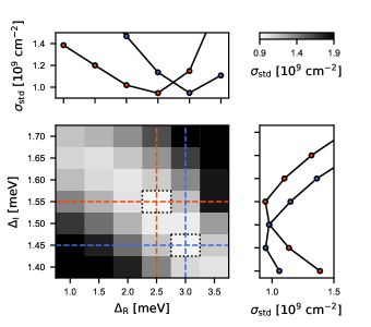
where is the number of data points, is the experimental value of the density difference and is the expectation value. The resulting standard deviation is depicted in Extended Data Fig.V. Notably, two minima with comparable standard deviations are observed for distinct parameter sets, marked by the red and blue dashed lines, respectively. Despite the marginal disparity, we opt for the parameter combination corresponding to the minimum standard deviation (red dashed lines) to determine the SOC parameters, specifically and .
.6 Interlayer screening
Due to the wave function polarization in BLG, interlayer screening effects reduce the effective interlayer potential. Here, we consider the effect of interlayer screening and calcualte the conversion between the interlayer potential energy and the displacement field at charge neutrality.
The interlayer potential energy [36]
| (15) |
is the result of an externally applied displacement field and an internal displacement field
| (16) |
Here, the screening density , being the electron density of layer , represents the difference between the electron density of the two graphene layers.
The screening density is obtained by first determining the layer-resolved density of states
| (17) |
where and are the wave functions of lattice site and on layer . Then the density is obtain by integration over the energy up to the Fermi energy :
| (18) |
The lower limit of the integration is set to , which is sufficiently large, such that in the range considered here.
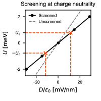
We calculate the screening density at charge neutrality point for interlayer potential energies , i.e. above , and calculate the corresponding displacement field according to
| (19) |
The result is shown in Extended Data Fig.VI as black dots. In this limited displacement field range, the function is linear and its slope is reduced by compared to the unscreened solution (dashed line). The critical interlayer potential energy difference translates into a critical displacement field , matching the result of our experiment.
References
- Burkard et al. [2023] G. Burkard, T. D. Ladd, A. Pan, J. M. Nichol, and J. R. Petta, Semiconductor spin qubits, Rev. Mod. Phys. 95, 025003 (2023).
- Rashba and Efros [2003] E. I. Rashba and A. L. Efros, Orbital mechanisms of electron-spin manipulation by an electric field, Phys. Rev. Lett. 91, 126405 (2003).
- Khoo et al. [2017] J. Y. Khoo, A. F. Morpurgo, and L. Levitov, On-demand spin–orbit interaction from which-layer tunability in bilayer graphene, Nano Letters 17, 7003 (2017).
- Avsar et al. [2020] A. Avsar, H. Ochoa, F. Guinea, B. Özyilmaz, B. van Wees, and I. Vera-Marun, Colloquium: Spintronics in graphene and other two-dimensional materials, Reviews of Modern Physics 92, 021003 (2020), publisher: American Physical Society.
- Trauzettel et al. [2007] B. Trauzettel, D. V. Bulaev, D. Loss, and G. Burkard, Spin qubits in graphene quantum dots, Nature Physics 3, 192 (2007).
- Gächter et al. [2022] L. M. Gächter, R. Garreis, J. D. Gerber, M. J. Ruckriegel, C. Tong, B. Kratochwil, F. K. de Vries, A. Kurzmann, K. Watanabe, T. Taniguchi, T. Ihn, K. Ensslin, and W. W. Huang, Single-shot spin readout in graphene quantum dots, PRX Quantum 3, 020343 (2022).
- Garreis et al. [2024] R. Garreis, C. Tong, J. Terle, M. J. Ruckriegel, J. D. Gerber, L. M. Gächter, K. Watanabe, T. Taniguchi, T. Ihn, K. Ensslin, and W. W. Huang, Long-lived valley states in bilayer graphene quantum dots, Nature Physics , 1 (2024).
- Denisov et al. [2024] A. O. Denisov, V. Reckova, S. Cances, M. J. Ruckriegel, M. Masseroni, C. Adam, C. Tong, J. D. Gerber, W. W. Huang, K. Watanabe, T. Taniguchi, T. Ihn, K. Ensslin, and H. Duprez, Ultra-long relaxation of a kramers qubit formed in a bilayer graphene quantum dot (2024), arXiv:2403.08143 [cond-mat, physics:quant-ph] .
- Kane and Mele [2005] C. L. Kane and E. J. Mele, Quantum spin hall effect in graphene, Phys. Rev. Lett. 95, 226801 (2005).
- Sichau et al. [2019] J. Sichau, M. Prada, T. Anlauf, T. J. Lyon, B. Bosnjak, L. Tiemann, and R. H. Blick, Resonance microwave measurements of an intrinsic spin-orbit coupling gap in graphene: A possible indication of a topological state, Phys. Rev. Lett. 122, 046403 (2019).
- Duprez et al. [2023] H. Duprez, S. Cances, A. Omahen, M. Masseroni, M. J. Ruckriegel, C. Adam, C. Tong, J. Gerber, R. Garreis, W. Huang, L. Gächter, T. Taniguchi, K. Watanabe, T. Ihn, and K. Ensslin, Spectroscopy of a single-carrier bilayer graphene quantum dot from time-resolved charge detection (2023), arXiv: 2311.12949 [cond-mat] .
- Avsar et al. [2014] A. Avsar, J. Y. Tan, T. Taychatanapat, J. Balakrishnan, G. K. W. Koon, Y. Yeo, J. Lahiri, A. Carvalho, A. S. Rodin, E. C. T. O’Farrell, G. Eda, A. H. Castro Neto, and B. Özyilmaz, Spin–orbit proximity effect in graphene, Nature Communications 5, 4875 (2014).
- Wang et al. [2016] Z. Wang, D.-K. Ki, J. Y. Khoo, D. Mauro, H. Berger, L. S. Levitov, and A. F. Morpurgo, Origin and magnitude of ‘designer’ spin-orbit interaction in graphene on semiconducting transition metal dichalcogenides, Phys. Rev. X 6, 041020 (2016).
- Island et al. [2019] J. O. Island, X. Cui, C. Lewandowski, J. Y. Khoo, E. M. Spanton, H. Zhou, D. Rhodes, J. C. Hone, T. Taniguchi, K. Watanabe, L. S. Levitov, M. P. Zaletel, and A. F. Young, Spin–orbit-driven band inversion in bilayer graphene by the van der Waals proximity effect, Nature 571, 85 (2019).
- Zhang et al. [2023] Y. Zhang, R. Polski, A. Thomson, E. Lantagne-Hurtubise, C. Lewandowski, H. Zhou, K. Watanabe, T. Taniguchi, J. Alicea, and S. Nadj-Perge, Enhanced superconductivity in spin–orbit proximitized bilayer graphene, Nature 613, 268 (2023).
- Holleis et al. [2023] L. Holleis, C. L. Patterson, Y. Zhang, H. M. Yoo, H. Zhou, T. Taniguchi, K. Watanabe, S. Nadj-Perge, and A. F. Young, Ising Superconductivity and Nematicity in Bernal Bilayer Graphene with Strong Spin Orbit Coupling (2023), arXiv:2303.00742 [cond-mat].
- Gmitra and Fabian [2017] M. Gmitra and J. Fabian, Proximity effects in bilayer graphene on monolayer WSe2 : Field-effect spin valley locking, spin-orbit valve, and spin transistor, Physical Review Letters 119, 146401 (2017).
- Rashba [2009] E. I. Rashba, Graphene with structure-induced spin-orbit coupling: Spin-polarized states, spin zero modes, and quantum hall effect, Phys. Rev. B 79, 161409 (2009).
- Khoo and Levitov [2018] J. Y. Khoo and L. Levitov, Tunable quantum hall edge conduction in bilayer graphene through spin-orbit interaction, Physical Review B 98, 115307 (2018).
- Li and Koshino [2019] Y. Li and M. Koshino, Twist-angle dependence of the proximity spin-orbit coupling in graphene on transition-metal dichalcogenides, Physical Review B 99, 075438 (2019).
- David et al. [2019] A. David, P. Rakyta, A. Kormányos, and G. Burkard, Induced spin-orbit coupling in twisted graphene–transition metal dichalcogenide heterobilayers: Twistronics meets spintronics, Physical Review B 100, 085412 (2019).
- Naimer et al. [2021] T. Naimer, K. Zollner, M. Gmitra, and J. Fabian, Twist-angle dependent proximity induced spin-orbit coupling in graphene/transition metal dichalcogenide heterostructures, Physical Review B 104, 195156 (2021).
- Chou et al. [2022] Y.-Z. Chou, F. Wu, and S. Das Sarma, Enhanced superconductivity through virtual tunneling in bernal bilayer graphene coupled to WSe2, Physical Review B 106, L180502 (2022).
- Yang et al. [2017] B. Yang, M. Lohmann, D. Barroso, I. Liao, Z. Lin, Y. Liu, L. Bartels, K. Watanabe, T. Taniguchi, and J. Shi, Strong electron-hole symmetric Rashba spin-orbit coupling in graphene/monolayer transition metal dichalcogenide heterostructures, Physical Review B 96, 041409 (2017).
- Zihlmann et al. [2018] S. Zihlmann, A. W. Cummings, J. H. Garcia, M. Kedves, K. Watanabe, T. Taniguchi, C. Schönenberger, and P. Makk, Large spin relaxation anisotropy and valley-Zeeman spin-orbit coupling in /graphene/-BN heterostructures, Physical Review B 97, 075434 (2018).
- Wang et al. [2019] D. Wang, S. Che, G. Cao, R. Lyu, K. Watanabe, T. Taniguchi, C. N. Lau, and M. Bockrath, Quantum Hall Effect Measurement of Spin–Orbit Coupling Strengths in Ultraclean Bilayer Graphene/WSe2 Heterostructures, Nano Letters 19, 7028 (2019).
- Sun et al. [2023] L. Sun, L. Rademaker, D. Mauro, A. Scarfato, A. Pásztor, I. Gutiérrez-Lezama, Z. Wang, J. Martinez-Castro, A. F. Morpurgo, and C. Renner, Determining spin-orbit coupling in graphene by quasiparticle interference imaging, Nature Communications 14, 3771 (2023).
- Wang et al. [2015] Z. Wang, D.-K. Ki, H. Chen, H. Berger, A. H. MacDonald, and A. F. Morpurgo, Strong interface-induced spin–orbit interaction in graphene on WS2, Nature Communications 6, 8339 (2015).
- Wakamura et al. [2019] T. Wakamura, F. Reale, P. Palczynski, M. Q. Zhao, A. T. C. Johnson, S. Guéron, C. Mattevi, A. Ouerghi, and H. Bouchiat, Spin-orbit interaction induced in graphene by transition metal dichalcogenides, Physical Review B 99, 245402 (2019).
- Fülöp et al. [2021] B. Fülöp, A. Márffy, S. Zihlmann, M. Gmitra, E. Tóvári, B. Szentpéteri, M. Kedves, K. Watanabe, T. Taniguchi, J. Fabian, C. Schönenberger, P. Makk, and S. Csonka, Boosting proximity spin–orbit coupling in graphene/WSe2 heterostructures via hydrostatic pressure, npj 2D Materials and Applications 5, 10.1038/s41699-021-00262-9 (2021).
- Bergemann [2005] C. Bergemann, Fermi surface measurements, in Encyclopedia of Condensed Matter Physics, edited by F. Bassani, G. L. Liedl, and P. Wyder (Elsevier, 2005) pp. 185–192.
- Rhodes et al. [2019] D. Rhodes, S. H. Chae, R. Ribeiro-Palau, and J. Hone, Disorder in van der waals heterostructures of 2d materials, Nature Materials 18, 541 (2019).
- Yankowitz et al. [2019] M. Yankowitz, Q. Ma, P. Jarillo-Herrero, and B. J. LeRoy, van der Waals heterostructures combining graphene and hexagonal boron nitride, Nature Reviews Physics 1, 112 (2019).
- Note [1] Note1, We acknowledge that the numerical outcome of the fit can be subtly influenced by the choice of the tight-binding intralayer and interlayer coupling parameters of BLG, referred to as the Slonczewski–Weiss–McClure parameters ( and ). These parameters dictate the curvature of the bands, thereby affecting the conversion between energy and density, as elaborated in detail in Methods .5. In addition, we chose to neglect the parameter , which governs the particle-hole asymmetry. This decision was made because including would introduce an offset between the electron and hole doping that is not observed in our experiments.
- Note [2] Note2, A recent experiment by Seiler et al. [56] in high-quality BLG demonstrated that trigonal warping causes the overlap (approximately ) of conduction and valence bands, resulting in a semi-metallic phase. Due to the band overlap, a finite displacement field is necessary to suppress the density of states at charge neutrality (CN) and open the band gap. However, this effect does not lead to a non-monotonic dependence of the conductivity, as observed in our experiment.
- McCann and Koshino [2013] E. McCann and M. Koshino, The electronic properties of bilayer graphene, Rep. Prog. Phys. 76, 056503 (2013).
- Kharitonov [2012a] M. Kharitonov, Canted antiferromagnetic phase of the quantum hall state in bilayer graphene, Physical Review Letters 109, 046803 (2012a).
- Maher et al. [2013] P. Maher, C. R. Dean, A. F. Young, T. Taniguchi, K. Watanabe, K. L. Shepard, J. Hone, and P. Kim, Evidence for a spin phase transition at charge neutrality in bilayer graphene, Nature Physics 9, 154 (2013).
- Nandkishore and Levitov [2010a] R. Nandkishore and L. Levitov, Flavor symmetry and competing orders in bilayer graphene (2010a), arXiv:1002.1966 [cond-mat] .
- Knothe and Jolicoeur [2016] A. Knothe and T. Jolicoeur, Phase diagram of a graphene bilayer in the zero-energy landau level, Phys. Rev. B 94, 235149 (2016).
- Weitz et al. [2010] R. T. Weitz, M. T. Allen, B. E. Feldman, J. Martin, and A. Yacoby, Broken-Symmetry States in Doubly Gated Suspended Bilayer Graphene, Science 330, 812 (2010).
- Kharitonov [2012b] M. Kharitonov, Antiferromagnetic state in bilayer graphene, Phys. Rev. B 86, 195435 (2012b).
- Gorbar et al. [2010] E. V. Gorbar, V. P. Gusynin, and V. A. Miransky, Energy gaps at neutrality point in bilayer graphene in a magnetic field, JETP Letters 91, 314 (2010).
- Tőke and Fal’ko [2011] C. Tőke and V. I. Fal’ko, Intra-landau-level magnetoexcitons and the transition between quantum hall states in undoped bilayer graphene, Phys. Rev. B 83, 115455 (2011).
- Wakamura et al. [2018] T. Wakamura, F. Reale, P. Palczynski, S. Guéron, C. Mattevi, and H. Bouchiat, Strong anisotropic spin-orbit interaction induced in graphene by monolayer , Phys. Rev. Lett. 120, 106802 (2018).
- Tiwari et al. [2021] P. Tiwari, S. K. Srivastav, and A. Bid, Electric-field-tunable valley zeeman effect in bilayer graphene heterostructures: Realization of the spin-orbit valve effect, Phys. Rev. Lett. 126, 096801 (2021).
- Amann et al. [2022] J. Amann, T. Völkl, T. Rockinger, D. Kochan, K. Watanabe, T. Taniguchi, J. Fabian, D. Weiss, and J. Eroms, Counterintuitive gate dependence of weak antilocalization in bilayer heterostructures, Phys. Rev. B 105, 115425 (2022).
- Konschuh et al. [2012] S. Konschuh, M. Gmitra, D. Kochan, and J. Fabian, Theory of spin-orbit coupling in bilayer graphene, Phys. Rev. B 85, 115423 (2012).
- Velasco et al. [2012] J. Velasco, L. Jing, W. Bao, Y. Lee, P. Kratz, V. Aji, M. Bockrath, C. N. Lau, C. Varma, R. Stillwell, D. Smirnov, F. Zhang, J. Jung, and A. H. MacDonald, Transport spectroscopy of symmetry-broken insulating states in bilayer graphene, Nature Nanotechnology 7, 156 (2012).
- Zhang et al. [2010] F. Zhang, H. Min, M. Polini, and A. H. MacDonald, Spontaneous inversion symmetry breaking in graphene bilayers, Phys. Rev. B 81, 041402 (2010).
- Nandkishore and Levitov [2010b] R. Nandkishore and L. Levitov, Dynamical screening and excitonic instability in bilayer graphene, Phys. Rev. Lett. 104, 156803 (2010b).
- Kharitonov and Efetov [2010] M. Y. Kharitonov and K. B. Efetov, Excitonic condensation in a double-layer graphene system, Semiconductor Science and Technology 25, 034004 (2010).
- Throckmorton and Das Sarma [2014] R. E. Throckmorton and S. Das Sarma, Quantum multicriticality in bilayer graphene with a tunable energy gap, Phys. Rev. B 90, 205407 (2014).
- Zhang et al. [2008] L. M. Zhang, Z. Q. Li, D. N. Basov, M. M. Fogler, Z. Hao, and M. C. Martin, Determination of the electronic structure of bilayer graphene from infrared spectroscopy, Phys. Rev. B 78, 235408 (2008).
- Jung and MacDonald [2014] J. Jung and A. H. MacDonald, Accurate tight-binding models for the bands of bilayer graphene, Phys. Rev. B 89, 035405 (2014).
- Seiler et al. [2023] A. M. Seiler, N. Jacobsen, M. Statz, N. Fernandez, F. Falorsi, K. Watanabe, T. Taniguchi, Z. Dong, L. S. Levitov, and R. T. Weitz, Probing the tunable multi-cone bandstructure in bernal bilayer graphene (2023), arXiv:2311.10816 [cond-mat] .
Acknowledgments
We thank Thomas Weitz, Anna Seiler, and Patrick Lee for fruitful discussions. We thank Peter Märki, Thomas Bähler, as well as the FIRST staff for their technical support. We acknowledge support from the European Graphene Flagship Core3 Project, Swiss National Science Foundation via NCCR Quantum Science, and H2020 European Research Council (ERC) Synergy Grant under Grant Agreement 95154. N.J. acknowledges funding from the International Center for Advanced Studies of Energy Conversion (ICASEC). K.W. and T.T. acknowledge support from the JSPS KAKENHI (Grant Numbers 20H00354 and 23H02052) and World Premier International Research Center Initiative (WPI), MEXT, Japan.
Data availability
Source data and analysis scripts associated with this study are made available via the ETH Research Collection (https://doi.org/10.3929/ethz-b-000662935).
Author contributions
M.M., H.D., T.I., K.E. conceived and designed the experiments. M.M., M.G., F.F, performed and analysed the measurements with inputs from H.D., J.G., and M.N.. M.M. designed the figures with inputs from C.T. and H.D.. M.M. and M.G. fabricated the device with inputs from J.G., M.N. and H.D.. A.P., N.J., L.L. provided theoretical support. T.T., K.W. supplied the hexagonal boron nitride. M.M wrote the manuscript with inputs from H.D.. All the coauthors mentioned above read and commented on the manuscript.