l
Authors to whom correspondence should be addressed: ] ssyeh@nycu.edu.tw (S.S.Y.) and jjlin@nycu.edu.tw (J.J.L.)
Authors to whom correspondence should be addressed: ] ssyeh@nycu.edu.tw (S.S.Y.) and jjlin@nycu.edu.tw (J.J.L.)
Giant Hall effect in two-dimensional CoSi2 granular arrays
Abstract
Granular metals offer tailorable electronic properties and play crucial roles in device and sensor applications. We have fabricated a series of nonmagnetic granular CoSi2 thin films and studied the Hall effect and transport properties. We observed a two orders of magnitude enhancement in the Hall coefficient in films fall slightly above the metal-insulator transition. This giant Hall effect (GHE) is ascribed to the local quantum-interference effect induced reduction of the charge carriers. Transmission electron microscopy images and transport properties indicate that our films form two-dimensional granular arrays. The GHE may provide useful and sensitive applications.
I Introduction
Granular metals, , are composites comprising metals () and insulators (), where denotes the volume or area fraction of .B. Abeles and Arie (1975) In granular composites, the size of metallic particles typically ranges from a few to hundreds of nanometers. Granular metals are inhomogeneously disordered, which forms either three-dimensional (3D) or two-dimensional (2D) arrays, depending on the metal grain size relative to film thickness. They can be considered as artificial solids with engineerable electronic and optical characteristics.Beloborodov et al. (2007) They serve as not only useful materials for nanotechnology applications but also controllable systems for exploring the quantum-interference and electron-electron interaction (EEI) effectsBeloborodov et al. (2007); Zhang et al. (2001a) as well as the percolation problem.B. Abeles and Arie (1975) In practice, research on granular composites has led to the development of chemical sensors,van Lith et al. (2007); Müller et al. (2011) strain gauges,Herrmann et al. (2007); Huth (2010) temperature-insensitive resistors,Yajadda et al. (2011) etc.
The Hall coefficient provides important information about the charge carrier density () and polarity in a conductor. The knowledge of of granular metals, especially its behavior in the vicinity of the percolation threshold or the metal-insulator transition (MIT), is of particular interest. According to the classical percolation theory, is sensitive to the dimensionality of the system.Shklovskii (1977); Bergman et al. (1983); Straley (1980); Juretschke et al. (1956) In 3D, the theory predicts that as decreases from 1, monotonically increases and takes a maximum value at the classical percolation threshold (). In 2D, the theory predicts that retains the same value of that of the pure metal in the entire metallic regime (). These classical predictions for the 3D caseBandyopadhyay et al. (1982) and 2D casePalevski et al. (1984) were previously observed in experiments. In this work, we report a finding of an enhancement by a factor 100 of as approaches the quantum percolation threshold, denoted by (), in a series of CoSi2 thin films which form 2D granular arrays. To our knowledge, such giant Hall effect (GHE) in 2D granular arrays has never been previously found. We interpret that the GHE arises from a reduction of due to the carrier localization induced by the local quantum interference effect in an inhomogeneously disordered systems containing rich microstructures.Zhang et al. (2001b) We mention that a continuous CoSi2 film is a good metal with its temperature () behavior of resistivity well described by the Boltzmann transport equation, until it undergoes superconducting at about 1.5 K.Chiu et al. (2024)
II Experimental Method
A series of CoSi2 thin films with various thicknesses, and thus grain sizes, were grown on 300-nm-thick SiO2 capped Si substrates. A Si layer with thickness was deposited on the substrate via thermal evaporation in a high vacuum ( torr), followed by the evaporation deposition of a Co layer of thickness . The ratio was chosen to ensure a complete reaction between Co and Si to form the CoSi2 phase in subsequent thermal annealing process.Chiu et al. (2017) After the thermal annealing process, the thickness of the resulted CoSi2 film was expected to be 3.5 , as previously established.van Ommen et al. (1988) This series of films, called group A, had thickness in the range nm and form a 2D granular array. A second series of CoSi2 films, called group B, with nm was grown via the deposition of a thick Co layer directly on a high-purity Si(100) substrate. The as-deposited groups A and B films were annealed in a high vacuum ( torr) at 600–800∘C for 1 h to form the CoSi2 phase. The CoSi2 structure was polycrystalline in group A, while nominally epitaxial in group B.Chiu et al. (2017) To facilitate transport measurements, a metal shadow mask was used during the deposition process to define a Hall bar geometry of 1 mm wide and 1 mm long. The relevant parameters of our films are listed in Table 1.
The topology of the CoSi2 film surface was characterized by the atomic force microscopy (AFM) (DFM SPA 400). The cross-sectional transmission electron microscopy (TEM) studies were performed using a high resolution transmission electron microscope (JEOL JEM-F200). Four-probe electrical and Hall effect measurements were carried out using a closed-cycle refrigerator and a 3He fridge.
III Results and Discussion
III.1 Giant Hall effect in 2D CoSi2 granular arrays
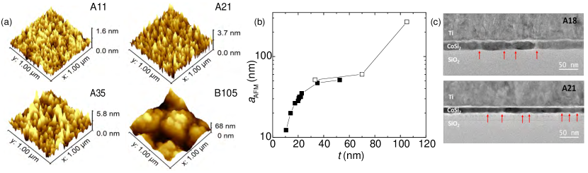
In Fig. 1(a), the surface topography for three group A and one group B CoSi2 films measured by AFM reveals mountain peak-like profiles. Assuming these peaks reflect the profiles of the surfaces of the constituent grains and grains are spherical, we estimate the grain size () in each film using the Gwyddion software (version 2.61). The data gathered from the AFM images were first leveled by mean plane subtraction, followed by row aligning using the median and matching methods. Horizontal scars or strokes were corrected to ensure accuracy, followed by color mapping to aid in selecting the appropriate range for analysis. Individual grains were then identified by selecting a threshold height of 50 percent, and all grain sizes within a 1-m2 area were measured and averaged. The obtained values are listed in Table 1.
Figure 1(b) shows the variation of with . For the B105 film, we obtain 330 nm, which is close to that determined from the scanning electron microscopy (SEM) and the TEM images.Chiou et al. (2015) For group A films, as increases from 11 to 52 nm, increases from 12 to 50 nm. For group B films, as increases from 33 to 105 nm, increases from 50 to 330 nm. We note that, in every film, . This implies that all of our films are constituted of a single layer of CoSi2 grains. The TEM images in Fig. 1(c) and those from our previous workChiou et al. (2015) also confirm this assertion. Thus, our CoSi2 films form 2D granular arrays (see further discussion below).
We have measured the longitudinal resistivity and of our films and obtained from . The Hall effect measurements indicate that the charge carriers are holes, in consistency with our previous resultsChiu et al. (2017, 2024) and band structure calculations.Mattheiss and Hamann (1988); Newcombe and Lonzarich (1988) The elastic electron mean free path is then calculated through , with the Fermi wavenumber . The value of the product for every film is listed in Table 1. Figure 2 shows the normalized resistivity, , as a function of for several group A films between 2 and 10 K. We see that those films having nm exhibit metallic behavior, i.e., increases with increasing ; while those films having nm reveal insulating behavior, i.e., decreases with increasing . Thus, the metal-insulator transition occurs around nm. In other words, for films with nm, the neighboring CoSi2 grains are geometrically connected, forming a percolating conduction array. For films with nm, the CoSi2 grains are geometrically disconnected. The inset of Fig. 2 shows (2 K) as a function of . As decreases from 53 to 11 nm, (2 K) increases rapidly from 131 to 4230 cm, indicating that the granularity plays an increasingly important role especially when decreases to below about 20 nm. For comparison, (2 K) = 4.55, 2.70 and 2.50 cm for nominally continuous films B33, B70 and B105, respectively.
| Film | (nm) | (nm) | (2 K) (nm) | |
|---|---|---|---|---|
| A11 | 11 | 12 | 1.0 | 40 |
| A14 | 14 | 20 | 1.5 | 38 |
| A18 | 18 | 26 | 3.1 | 47 |
| A20 | 20 | 28 | 5.1 | 40 |
| A20.5 | 20.5 | 30 | 8.3 | – |
| A21 | 21 | 32 | 10 | 57 |
| A22 | 22 | 32 | 10 | – |
| A23 | 23 | 35 | 11 | 69 |
| A35 | 35 | 47 | 21 | 100 |
| A52 | 52 | 51 | 24 | 130 |
| B33 | 33 | 52 | 310 | 690 |
| B70 | 70 | 60 | 510 | 1300 |
| B105 | 105 | 330 | 540 | 1400 |
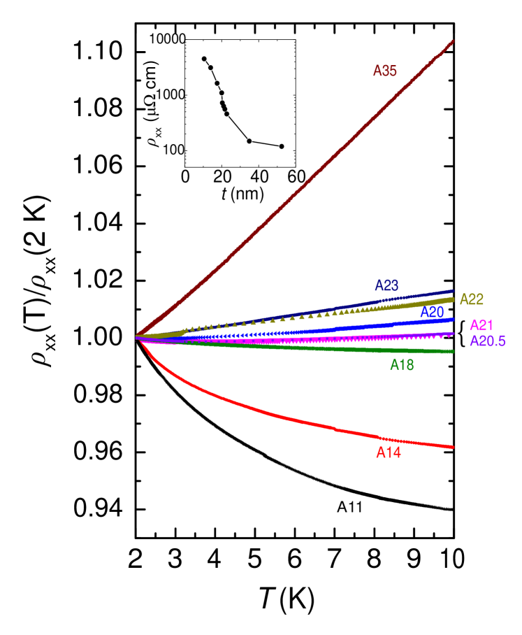
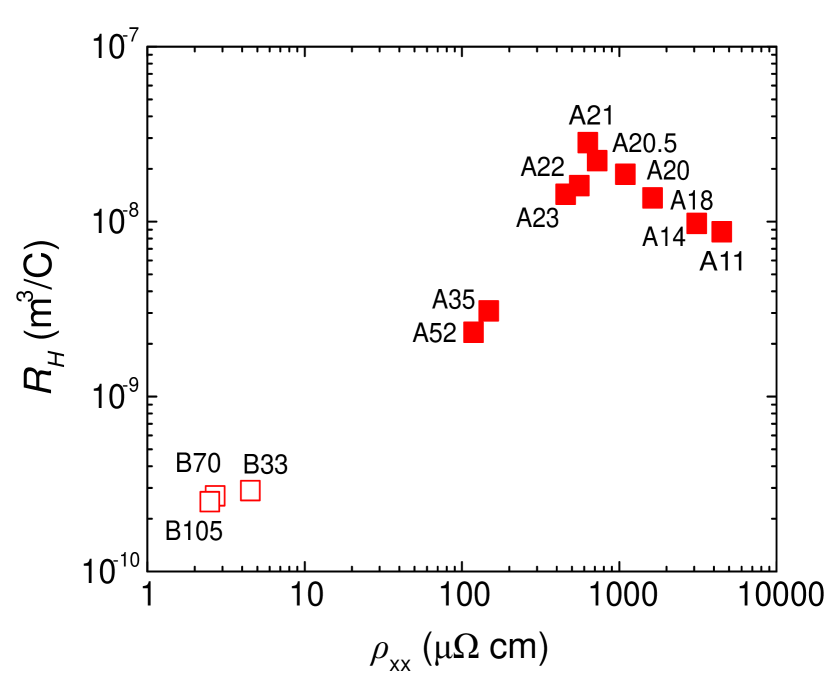
Figure 3 shows as a function of at = 2 K. The thickest film B105 has the lowest Hall coefficient 2.5 m3/C, in agreement with the previous result.Radermacher et al. (1993); Van Ommen et al. (1990) This film will serve as our reference film with the value for a good CoSi2 metal. Note that for films A21–A52, monotonically increases with increasing , reaching a maximum value of 2.8 m3/C (corresponding to 2.2 m-3) in film A21. This is a film falling just above the MIT. Interestingly, as () further increases (decreases), progressively decreases to 8.7 m3/C in film A11, which falls below the MIT. We emphasize that the value of film A21 is 100 times larger than that of film B105. This is the GHE.Wan and Sheng (2002) Recall that according to the classical percolation theory,Zhang et al. (2001b); Wu et al. (2010) will be enhanced by a factor , where is the critical exponent of Hall resistivity, is the exponent of the correlation length, and is the grain size. However, for a 2D percolation system, (Ref. Straley, 1980) and (Ref. Bergman and Stroud, 1992), thus should remain a constant in the entire metallic regime (), as mentioned.Shklovskii (1977); Bergman et al. (1983); Straley (1980); Juretschke et al. (1956) This prediction was confirmed by a previous study of 2D granular Au films.Palevski et al. (1984) On the other hand, = 0.4 and = 0.9 in 3D, thus an enhancement of by a factor of 10 is expected for, e.g., a thick granular film with = 1 m and = 10 nm. The GHE means that the measured value is orders of magnitude larger than the classical value.
Wan and ShengWan and Sheng (2002) have developed a quantum percolation theory which considers the wave nature of the charge carriers in a 3D nonmagnetic granular system. At low , when the electron dephasing length is larger than the feature size () of the microstructures, the carrier wavefunctions will undergo multiple scattering in the random percolating clusters of the conducting channels until a phase-breaking event takes place. Such multiple coherent scattering leads to a local quantum-interference effect which causes significant localization of carrier wavefunctions as . Consequently, will be greatly reduced, which in turn gives rise to a greatly enhanced at . This theory has successfully explained the GHE observed in 3D Cux(SiO2)1-x compositesZhang et al. (2001b) and Mox(SnO2)1-x composites,Wu et al. (2010) where an enhancement by a factor of nearly three orders of magnitude in was observed. Due to this local quantum interference effect, which is absent in the classical percolation theory, peaks at a metal volume fraction . The GHE in 2D has not been theoretically treated in the literature.
To clarify the underlying physics for the GHE observed in our group A films, we have measured the weak-localization induced magnetoresistanceLin and Bird (2002) at low and extracted for each film, see Table 1. The (2 K) values in group B nominally epitaxial films are much longer than those in group A polycrystalline films, as expected. In both cases, decreases with decreasing , due to an increasing dephasing rate as the disorder is increased with decreasing and decreasing . Most important, we obtain (2 K) in all films. Consequently, multiple coherent electron scattering within a characteristic area of leads to a quasi-2D local quantum interference effect, resulting in a reduced and an enhanced .Zhang et al. (2001b); Wan and Sheng (2002)
In the percolation theory, the relevant parameter is the metal volume (area) fraction , which cannot be accurately determined in our films. Nevertheless, we know that occurs around 19 nm where the MIT takes place. On the other hand, we may assume occur around 21 nm where the value peaks. This is in consistency with the above quantum percolation theory prediction that .Wan and Sheng (2002) At this critical thickness, one expects the film have a value of the product , i.e., the Ioffe-Regel criterion, see Table 1. Thus, our observation of the 2D version of the GHE is satisfactorily understood.
III.2 Transport in 2D CoSi2 granular arrays
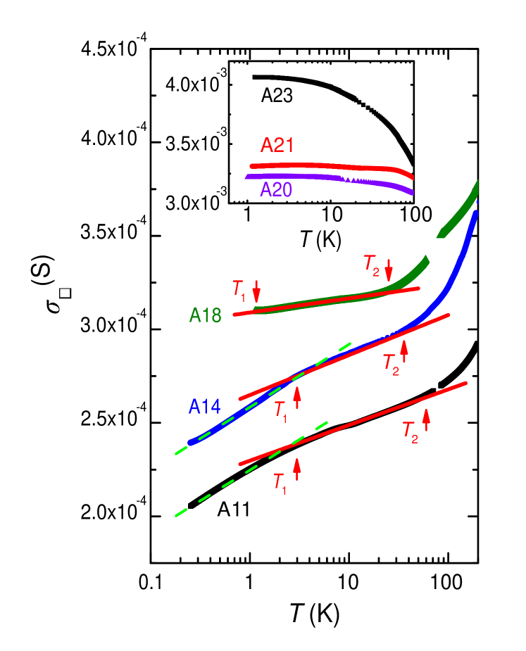
To further clarify the occurrence of the GHE and the array dimensionality () of group A films, we study their longitudinal transport behavior. Figure 4 shows the sheet conductivity as a function of for films A11, A14 and A18, which have . We find a dependence in the temperature regime , with 3, 3 and 1.2 K, and 60, 37 and 16 K, for films A11, A14 and A18, respectively. This behavior does not originate from the 2D EEI effect of Altshuler and Aronov (AA),Altshuler and Aronov (1985) which considers homogeneously disordered metals. To rule out this scenario, we may first assume our films be homogeneously disordered and calculate the thermal diffusion length , where is the diffusion constant, is the reduced Planck constant, and is the effective electron mass. (We take to be the free electron mass. Radermacher et al. (1993)) We obtain in the regime for films A11, A14 and A18. This implies that these films, if homogeneously disordered, should be 3D with regard to the AA EEI effect, then the conductivity correction must obey a temperature dependence.Altshuler and Aronov (1985) This is clearly not the case.
In fact, our results must be explained by the electron tunneling conduction in the presence the EEI effect in a granular array. In the strong intergranular coupling regime with , the transport properties of granular metals have been theoretically addressed,Beloborodov et al. (2007) where is a dimensionless tunneling conductance between neighboring grains, is a critical conductivity, is the charging energy with () being the permittivity of vacuum (dielectric constant of ), and is the mean energy level spacing in a grain. The granular metal theory predicts that, in the temperature regime ( is the Boltzmann constant), incoherent tunneling processes on scales approximately equal to the grain size play a pivotal role in governing the system conductivity, causing a conductivity correction (). As the temperature further decreases to , the coherent electron motion on scales larger than becomes important, causing another conductivity correction (). Thus, the total conductivity is given by , where is the conductivity without the EEI effect,
| (1) |
and, for = 2,
| (2) |
We note that the term reproduces the AA EEI effect by taking the screening factor to be zero.
Figures 4 shows that our results can be well described by the predictions (red straight lines) of Eq. (1) in the intermediate regime. For a quantitative analysis, we may take (Ref. Sun et al., 2010) and to estimate .111We use in this estimation, which is the average of the dielectric constants of vacuum and SiO2. The value thus obtained (see Table 2) is comparable with the corresponding value. From the fitted and values, the values can calculated with , where is the density of states (DOS) at the Fermi energy of the free-electron model. The values can also be calculated. We obtain and for each film, supporting the interpretation in terms of the correction. Moreover, below , a crossover to the correction is observed in the two most granular films, A11 and A14, as indicated by the fitted green dashed straight lines given by Eq. (2).222If we rewrite Eq. (2) into the more familiar AA expression and fit the data at to this equation, we obtain () for film A11 (A14). Thus, the results of Fig. 4 over the wide temperature from 0.25 K to indicate that our films form 2D, rather than 3D, granular arrays. This conclusion is in line with the 2D granular array structure determined from the AFM and TEM images discussed above.
| Film | (K) | (nm) | (K) | |
|---|---|---|---|---|
| A11 | 600 | 11 | 2.8 | 6.6 |
| A14 | 370 | 18 | 4.4 | 2.5 |
| A18 | 160 | 42 | 27 | 1.3 |
The inset of Fig. 4 shows that films A20, 21 and 23 reveal metallic behavior, with increasing with decreasing . This result further supports the GHE theory prediction that should peak at . Furthermore, we note that the large enhancement in film A21 cannot be ascribed to the suppression of DOS. The granular metal theory has calculated the corrections to the DOS due to the EEI effect in the presence of granularity.Efetov and Tschersich (2003); Beloborodov et al. (2003) For = 2 and at , the correction to the DOS at the Fermi energy () is given by . This result indicates that a smaller grain size (a larger ) and a smaller will cause a larger . Consider, for example, film A18. From the values 160 K and 27, we estimate , which would lead to a 3% increase in through the relation , where is a correction to . For the more continuous and less granular film A21, should be smaller than that in film A18. This small correction of DOS certainly cannot explain the observed GHE.
IV Conclusion
We have fabricated a series of two-dimensional granular CoSi2 films which encompasses the metal-insulator transition. We observe an enhanced Hall coefficient by a factor of 100, which occurs in a film falling slightly above the metal-insulator transition. We explain this result in terms of the giant Hall effect due to the local quantum-interference effect induced reduction of charge carriers. The two dimensionality of our granular arrays is confirmed by transmission electron microscopy studies and low-temperature transport properties. Granular CoSi2 films are stable under ambient conditions. Their large Hall effect may benefit useful and sensitive applications.
Acknowledgements.
This work was supported by the National Science and Technology Council of Taiwan through grant numbers 110-2112-M-A49-015 and 111-2119-M-007-005 (J.J.L.), and 110-2112-M-A49-033-MY3 (S.S.Y.). S.S.Y. was partly supported by the Center for Emergent Functional Matter Science of NYCU from The Featured Areas Research Center Program within the framework of the Higher Education Sprout Project by the Ministry of Education of Taiwan. The authors acknowledge the use of HRTEM at the Instrument Center of National Tsing Hua University (Taiwan).References
- B. Abeles and Arie (1975) M. C. B. Abeles, Ping Sheng and Y. Arie, Advances in Physics 24, 407 (1975), https://doi.org/10.1080/00018737500101431 .
- Beloborodov et al. (2007) I. S. Beloborodov, A. V. Lopatin, V. M. Vinokur, and K. B. Efetov, Reviews of Modern Physics 79, 469 (2007).
- Zhang et al. (2001a) Y.-J. Zhang, Z.-Q. Li, and J.-J. Lin, Physical Review B 84, 052202 (2001a).
- van Lith et al. (2007) J. van Lith, A. Lassesson, S. A. Brown, M. Schulze, J. G. Partridge, and A. Ayesh, Applied Physics Letters 91, 181910 (2007), https://pubs.aip.org/aip/apl/article-pdf/doi/10.1063/1.2802730/14382618/181910_1_online.pdf .
- Müller et al. (2011) K.-H. Müller, E. Chow, L. Wieczorek, B. Raguse, J. S. Cooper, and L. J. Hubble, Physical Chemistry Chemical Physics 13, 18208 (2011).
- Herrmann et al. (2007) J. Herrmann, K.-H. Müller, T. Reda, G. R. Baxter, B. Raguse, G. J. J. B. de Groot, R. Chai, M. Roberts, and L. Wieczorek, Applied Physics Letters 91, 183105 (2007), https://pubs.aip.org/aip/apl/article-pdf/doi/10.1063/1.2805026/14381901/183105_1_online.pdf .
- Huth (2010) M. Huth, Journal of Applied Physics 107, 113709 (2010), https://pubs.aip.org/aip/jap/article-pdf/doi/10.1063/1.3443437/13198002/113709_1_online.pdf .
- Yajadda et al. (2011) M. M. A. Yajadda, I. Levchenko, and K. Ostrikov, Journal of Applied Physics 110, 023303 (2011), https://pubs.aip.org/aip/jap/article-pdf/doi/10.1063/1.3610497/15075216/023303_1_online.pdf .
- Shklovskii (1977) B. I. Shklovskii, Soviet Physics Journal of Experimental and Theoretical Physics 45, 152 (1977).
- Bergman et al. (1983) D. J. Bergman, Y. Kantor, D. Stroud, and I. Webman, Physical Review Letters 50, 1512 (1983).
- Straley (1980) J. P. Straley, Journal of Physics C: Solid State Physics 13, L773 (1980).
- Juretschke et al. (1956) H. J. Juretschke, R. Landauer, and J. A. Swanson, Journal of Applied Physics 27, 838 (1956), https://pubs.aip.org/aip/jap/article-pdf/27/7/838/18315858/838_1_online.pdf .
- Bandyopadhyay et al. (1982) B. Bandyopadhyay, P. Lindenfeld, W. L. McLean, and H. K. Sin, Physical Review B 26, 3476 (1982).
- Palevski et al. (1984) A. Palevski, M. Rappaport, A. Kapitulnik, A. Fried, and G. Deutscher, J. Physique Lett. 45, 367 (1984).
- Zhang et al. (2001b) X. X. Zhang, C. Wan, H. Liu, Z. Q. Li, P. Sheng, and J. J. Lin, Physical Review Letters 86, 5562 (2001b).
- Chiu et al. (2024) S.-P. Chiu, C.-J. Wang, Y.-C. Lin, S.-T. Tu, S. Sahu, R.-T. Wang, C.-Y. Wu, S.-S. Yeh, S. Kirchner, and J.-J. Lin, “Electronic conduction and superconducting properties of CoSi2 films on silicon – an unconventional superconductor with technological potential,” (2024), arXiv:2401.17601 [cond-mat.supr-con] .
- Chiu et al. (2017) S.-P. Chiu, S.-S. Yeh, C.-J. Chiou, Y.-C. Chou, J.-J. Lin, and C.-C. Tsuei, ACS Nano 11, 516 (2017).
- van Ommen et al. (1988) A. H. van Ommen, C. W. T. Bulle-Lieuwma, and C. Langereis, Journal of Applied Physics 64, 2706 (1988).
- Chiou et al. (2015) C.-J. Chiou, S.-P. Chiu, J.-J. Lin, and Y.-C. Chou, Crystal Engineering Communications 17, 4276 (2015).
- Mattheiss and Hamann (1988) L. F. Mattheiss and D. R. Hamann, Physical Review B 37, 10623 (1988).
- Newcombe and Lonzarich (1988) G. C. F. Newcombe and G. G. Lonzarich, Physical Review B 37, 10619 (1988).
- Radermacher et al. (1993) K. Radermacher, D. Monroe, A. E. White, K. T. Short, and R. Jebasinski, Phys. Rev. B 48, 8002 (1993).
- Van Ommen et al. (1990) A. H. Van Ommen, C. W. T. Bulle-Lieuwma, J. J. M. Ottenheim, and A. M. L. Theunissen, Journal of Applied Physics 67, 1767 (1990), https://pubs.aip.org/aip/jap/article-pdf/67/4/1767/8011497/1767_1_online.pdf .
- Wan and Sheng (2002) C. Wan and P. Sheng, Physical Review B 66, 075309 (2002).
- Wu et al. (2010) Y.-N. Wu, Z.-Q. Li, and J.-J. Lin, Physical Review B 82, 092202 (2010).
- Bergman and Stroud (1992) D. J. Bergman and D. Stroud (Academic Press, 1992) pp. 147–269.
- Lin and Bird (2002) J. J. Lin and J. P. Bird, Journal of Physics: Condensed Matter 14, R501 (2002).
- Altshuler and Aronov (1985) B. L. Altshuler and A. G. Aronov, in Electron–Electron Interactions in Disordered Systems, edited by A. L. Efros and M. Pollak (Elsevier, 1985) pp. 1–153.
- Sun et al. (2010) Y.-C. Sun, S.-S. Yeh, and J.-J. Lin, Physical Review B 82, 054203 (2010).
- Note (1) We use in this estimation, which is the average of the dielectric constants of vacuum and SiO2.
- Note (2) If we rewrite Eq. (2) into the more familiar AA expression and fit the data at to this equation, we obtain () for film A11 (A14).
- Efetov and Tschersich (2003) K. B. Efetov and A. Tschersich, Physical Review B 67, 174205 (2003).
- Beloborodov et al. (2003) I. S. Beloborodov, K. B. Efetov, A. V. Lopatin, and V. M. Vinokur, Physical Review Letters 91, 246801 (2003).