Picosecond Femtojoule Resistive Switching in Nanoscale VO2 Memristors
Abstract
Beyond-Moore computing technologies are expected to provide a sustainable alternative to the von Neumann approach not only due to their down-scaling potential but also via exploiting device-level functional complexity at the lowest possible energy consumption. The dynamics of the Mott transition in correlated electron oxides, such as vanadium dioxide, has been identified as a rich and reliable source of such functional complexity. However, its full potential in high-speed and low-power operation has been largely unexplored. We fabricated nanoscale VO2 devices embedded in a broad-band test circuit to study the speed and energy limitations of their resistive switching operation. Our picosecond time-resolution, real-time resistive switching experiments and numerical simulations demonstrate that tunable low-resistance states can be set by the application of 20 ps long, 1.7 V amplitude voltage pulses at 15 ps incubation times and switching energies starting from a few femtojoule. Moreover, we demonstrate that at nanometer-scale device sizes not only the electric field induced insulator-to-metal transition, but also the thermal conduction limited metal-to-insulator transition can take place at timescales of 100’s of picoseconds. These orders of magnitude breakthroughs open the route to the design of high-speed and low-power dynamical circuits for a plethora of neuromorphic computing applications from pattern recognition to numerical optimization.
Introduction
Few-component analog circuits exploiting the dynamical complexity of memristors enable increased functional complexity at a minimized footprint. Moreover, they can energy-efficiently replace extensive digital circuits designed to facilitate demanding algorithms [1, 2]. Meanwhile reconfigurability, a great asset of digital platforms, has been put forward also in the analog domain by the concept of memristive field-programmable analog arrays [3]. In particular, second order dynamical complexity arising from the Mott-type insulator-to-metal transition (IMT) [4, 5, 6, 7, 8, 9, 10] in NbO2 has been utilized to realize relaxation oscillators and chaotic dynamics for accelerating probabilistic optimization in transistor-less circuits [11, 12]. Passively coupled VO2 Mott-memristors have been used to mimic the fundamental adaptability of the biological nervous system to various input streams and even faithfully reproduce a spectrum of bio-realistic neural response patterns [13]. The phase information in coupled VO2 oscillator networks has been identified as a state variable and exploited in neural network operation [14, 15, 16, 17]. The discovery of short and longer enduring metallic domains enabled sub-threshold operation, short-term and long-term memory functionalities extending the toolkit for neuromorphic data storage and processing [18, 19].
The potential for high-speed and low-energy operation relying on the IMT in VO2 based devices has been predicted by theoretical considerations [5] and simulations [13]. Experiments carried out in the optical and THz domain [20, 21, 22, 23, 24, 25, 26] have demonstrated that due to its predominantly electronic origin, the IMT can indeed be completed at sub-picosecond time-scales. However, the more scalable electrical domain applications could so far only exploit 300 ps set and 1 ns reset switching times at 100 fJ energy costs [18, 27, 19].
Here we demonstrate that the resistive switching response of VO2 memristors to purely electrical stimuli can be as fast as 15 ps for the set transition, in agreement with finite element simulations based on a two-dimensional resistor network model. The evaluation of the current acquired during the applied 20 ps long voltage pulses reveals that the IMT is triggered by the injection of as little Joule heat as a few femtojoule. Furthermore, a dedicated V-shaped electrode arrangement is utilized to focus the electric field and, thus, the device operation to a nanometer-scale active volume. Consequently, the thermal relaxation time to the insulating state of VO2 can be greatly reduced to the 100 ps time-scale, enabling low-power dynamical memristor circuits for ultra-fast neuromorphic computing applications.
Results and Discussion
Our report is organized as follows. First, the device structure and the DC characterization of the resistive switching cycles are presented. Next, the transmission spectroscopy of sub-nanosecond voltage pulses is explained. Using this method, we demonstrate the analog tunability of the volatile low resistance states, set switching times down to 15 ps and switching energies in the femtojoule regime. We show that these results can be quantitatively understood in terms of a two-dimensional resistor network of nanometer-scale VO2 domains, where the resistance of each domain is determined by the local temperature and electric field. Finally, we use a pump-probe scheme utilizing 20 ps long voltage pulses to monitor the complete recovery of the high resistance state in the sub-nanosecond time-domain.
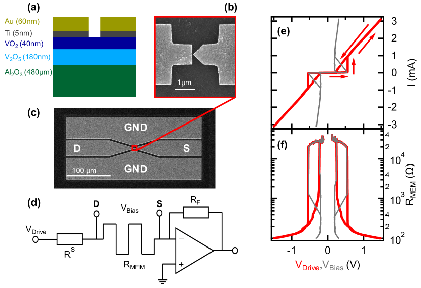
Device Structure and DC Characterization. The individual layer thicknesses of the sample are labeled in the schematic vertical cross-section in Fig. 1(a). The magnified top view of the planar device is exhibited in Fig. 1(b). The two, asymmetrically shaped Au electrodes were evaporated on the top of a VO2/V2O5 film, which was created by the thermal oxidation of a V layer evaporated on top of a sapphire substrate [10, 28]. The planar gap between the two electrodes was around 30 nm. The latter, together with the flat (triangular) shape of the source (drain) electrode, facilitate low-voltage resistive switching in a single, nanometer-scale volume of the underlying VO2 layer. Further details on sample fabrication and characterization are provided in the Methods and Experimental Section and in Ref. 10. Figure 1(c) shows the electrode layout of the devices. The source (S), drain (D) and the two ground (GND) electrodes made of 50 nm thick Au form a co-planar waveguide (CPW). The CPW ensures the suitable termination of the two-terminal Au/VO2/Au devices for the short-duration voltage pulses of the high-speed resistive switching experiments.
The DC characterization of the current-voltage [] traces were carried out in a setup consisting of a series resistor, the memristor device, a current amplifier and a data acquisition card which was also utilized as a programmable voltage source, as illustrated in Fig. 1(d) and explained in detail in the Methods and Experimental Section. In our nomenclature the voltage is applied on the device and the current limiting series resistor whereas the voltage drop on the memristor device only is denoted as . Positive voltage corresponds to higher potential on the drain electrode.
A representative, hysteretic trace exhibiting unipolar, volatile resistive switching is shown in Fig. 1(e) both as a function of (red) and (gray). The resistance, calculated as is plotted in Fig. 1(f). Resistive switching reproducibly occurs between typical high resistance states (HRS) of 30 k and tunable low resistance states (LRS) in the 102 – 103 regime at set (reset) voltages around 550 mV (250 mV). The actual value can be fine-tuned by the choice of and the power of the driving voltage signal. The reproducibility and endurance of the resistive switching cycles benefit from the well-defined, few 10 nm scale, presumably single-domain volume of the IMT [10].
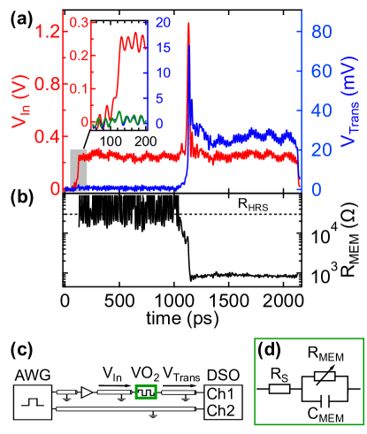
Picosecond Time-Scale Set Switching. The speed limit and energy consumption of resistive switching in VO2 memristors was investigated by the real-time monitoring of the devices’ resistive response to voltage pulses as short as 20 ps full width at half maximum (FWHM). Resistive switching taking place within 20 ps due to the injection of 1 – 5 fJ energy was demonstrated. The corresponding experimental setup is shown in Fig. 2(c) and described in the Methods and Experimental Section. The measurement technique and the data analysis followed the procedures explained in great detail in Ref. 29. In short, when the memristor device is exposed to fast voltage signals whose wavelength falls below the length of the utilized transmission lines, partial reflection and transmission of the incoming voltage signal occurs due to the impedance mismatch between the device impedance and the 50 wave impedance of the transmission lines. According to the solution of the telegraph equations applied to our experimental arrangement, the voltage drop on the sample equals to whereas the current equals to , where and are the amplitudes of the reflected and transmitted harmonic waves, respectively. The impedance of the memristor can be determined through the formula
| (1) |
where, in general, harmonic signals and a frequency dependent, complex-valued are assumed. When the memristor impedance is dominated by a frequency independent, real-valued resistive term, , Eq. 1 directly applies and is proportional to any time dependent signal. When a complex-valued, frequency dependent is concerned, the numerical deduction of the device impedance requires a model assumption on and a Fourier analysis based on Eq. 1.
A simplistic equivalent circuit accounting for the lead resistance and parasitic capacitance of the memristor is shown in Fig. 2(d). While the former contribution is usually negligible compared to the device resistance, and merely plays a role in the capacitive response time through the product, the frequency dependent capacitive impedance contribution arising from may have a profound impact on the real time response during the applied voltage pulses.
Figure 2(a) shows the measured response (blue, right axis) to a pulse sequence (red, left axis). The latter consists of a 1 ns long, low-amplitude read-out pulse, a 20 ps FWHM, 1.3 V amplitude set pulse and a second read-out pulse identical to the first one. The relative timing of and are compensated for the propagation time differences in the transmission lines according to the procedures outlined in Ref. 29. During the first read-out pulse the device resides in its HRS and stays low, consistently with Eq. 1 and 30 k. It is important to note the absence of a dominant capacitive peak in during the 20 ps rise time of the first read-out pulse, exhibited in the magnified view of the inset in Fig. 2(a). This observation evidences the negligible capacitive impedance of the device even in the HRS and indicates the purely resistive nature of the impedance switching. A quantitative analysis using LTspice shows a good agreement between the modeled (green) and measured (blue) signal in the voltage step region by assuming 2 fF. In contrast, a higher value would give rise to a dominant peak in response to the rising edge of , which is definitely not the case here.
Resistive switching due to the 20 ps FWHM set voltage pulse is demonstrated by the sharp increase of during the set pulse and the persistence of an increased transmission during the second, 1 ns long read-out period. In the absence of a prevailing capacitive contribution, e.g., during the constant voltage read-out periods, the device’s resistive impedance can be well approximated from the ratio based on Eq. 1, as shown in Fig. 2(b). Note, however, that the apparent rate of the such deduced resistance change within duration of the set pulse is instrumentally limited within the set pulse duration by the 60 GHz analog bandwidth of the detection setup. Additionally, within the duration of a short pulse the frequency dependent capacitive contribution to can no longer be neglected which further limits the validity of the quantitative analysis on in this time window [29].
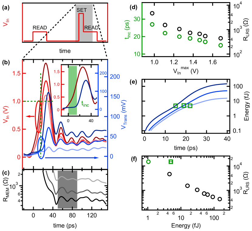
Next, we investigate the set switching dynamics in more detail by applying 20 ps FWHM set voltage pulses of different amplitudes and evaluating the resulting resistance change, switching times and switching energies. The applied pulse sequence is schematically illustrated in Fig. 3(a). In essence, a similar pattern is utilized as discussed in the demonstrator experiment shown in Fig. 2, only this time the first, 1 ns long and 0.25 V amplitude read-out pulse is shifted 100 ns away from the set pulse. As this time separation is much longer than the zero-bias relaxation time from the LRS to the HRS, a possible preconditioning of the set switching by the first read-out pulse can be unambiguously excluded.
Figure 3(b) exemplifies the response (blue colors, right axis) to 20 ps FWHM pulses (red colors, left axis) of three different amplitudes. The corresponding, time dependent resistance traces assessed from the ratio according to Eq. 1 are shown in Fig. 3(c). For further evaluation, the values are deduced by averaging over the gray shaded time window in Fig. 3(c). The fine analog tunability of the LRS is demonstrated in Fig. 3(d) where a 60% increase in results in the gradual, one order of magnitude decrease of in the 102 – 103 regime (black dots, right axis). This behavior is consistent with the set pulse energy dependent volume of the metal-insulator transition (MIT), as will be discussed later in the framework of our set switching model.
In addition to the decreasing tendency in , an apparent acceleration of the set transition is also observed at higher . We characterize the speed of the set process by the incubation time which is experimentally defined here as the time interval between the 10% onset of and reaching 15 k, as illustrated by the green shaded area in the inset of Fig. 3(b). The incubation time as a function of the applied setting is shown in Fig. 3(d) by the green dots (left axis). Although the Mott type IMT in VO2 is identified to have a dominant electronic origin and, thus, can be triggered even by femtosecond laser excitation [20], previous experiments utilizing voltage pulses have reported incubation times down to 100’s of picoseconds [19]. In contrast, we demonstrate incubation times down to 15 ps. Note, that the voltage pulse amplitude dependence does not show any saturation at this value, therefore values in the single digit picosecond regime are highly conceivable. However, the applied pulse amplitudes were restricted to 1.7 V in order to protect the devices from destruction.
The data presented in Fig. 3(b) also sheds light on the threshold switching nature of the set transition: the lower values deduced at higher settings correspond to the same actual 1 V voltage levels, as highlighted by the green dashed lines. The observed apparent dependence of in Fig. 3(d) is quantitatively accounted for by the instrumental aspects of our pulse firing setup, where the rise time of the voltage pulse is always 20 ps, independently of the pulse amplitude. Consequently, the same threshold voltage is established faster when a higher amplitude pulse is applied. Such a threshold switching behavior is in agreement with the models which attribute a purely electronic [4] or a mixed electronic and thermal origin [10] to the IMT in VO2. In contrast, ionic migration driven resistive switching compounds exhibit exponentially decreasing incubation times at linearly increasing voltage levels, known as the voltage-time dilemma [30, 31, 32]. Based on the above arguments, we argue that an independent control on and shall be possible in VO2 devices, as the former is merely governed by the rise time of the set pulse while the latter is determined by its amplitude and duration, i.e., the total set pulse energy, as demonstrated by the black circles in Fig. 3(d). Note, however, that 20 ps rise times at Volt-scale signal levels are facing the limitations of current state of the art electronics.
The set switching energies required to reach a specific were calculated by numerically integrating the product of the voltage drop on the sample and the current as a function of time, as shown by the solid lines in Fig. 3(e) for the three example time traces of Fig. 3(b). The corresponding incubation times are marked by the green squares. They highlight that the set transition is ignited after the injection of 5 fJ energy, independently of the specific shape of the set pulse, underpinning the role of local heating in the IMT. The Joule heating contribution is estimated to be 1 fJ, by taking the capacitive charging energy of 4 fJ into account, where 2 V and 2 fF.
The LRS resistance values deduced from the 40 ps long time interval directly following the falling edges of the different amplitude set pulses are plotted against the total energy deposited in the device by the black circles in Fig. 3(f). As a reference, the average and standard deviation of the total energies calculated at for the three example traces of Fig. 3(e) are also displayed in Fig. 3(f) by the green square and its error bar, respectively. According to our definition of , the corresponding resistance value is 15 k. Note, that the energy values of the black circles naturally exclude most of the capacitive charging energy, as they involve the time integral over the entire duration of the corresponding set pulses where the contributions of charging and discharging mostly cancel out. Therefore, these energy values can be directly attributed to the Joule heating contribution. The green circle extrapolates the tendency drawn by the black symbols to 15 k as an estimate of the set switching energy limitations for an ideally parasitic capacitance-free device design. In contrast, the energy value of the green square was determined at the onset of the set pulses, where the 4 fJ penalty of capacitive charging is not yet counteracted with the subsequent discharging. In comparison to the state of the art switching energies of 400 fJ in silicon CMOS neurons [33], 50 fJ in electrochemical metalization cells [34] and 100 fJ in valence change oxide memories [35, 36, 29] as well as in micrometer-scale VO2 samples [19], this evaluation demonstrates the merits of nanoscale VO2 devices in high-frequency electronics reaching single-digit femtojoule switching energies at k range LRSs. The latter regime quantitatively corresponds to the extreme energy efficiency of the human brain, where the energy cost of a neural spike is estimated to be 5 – 100 fJ [37, 13].
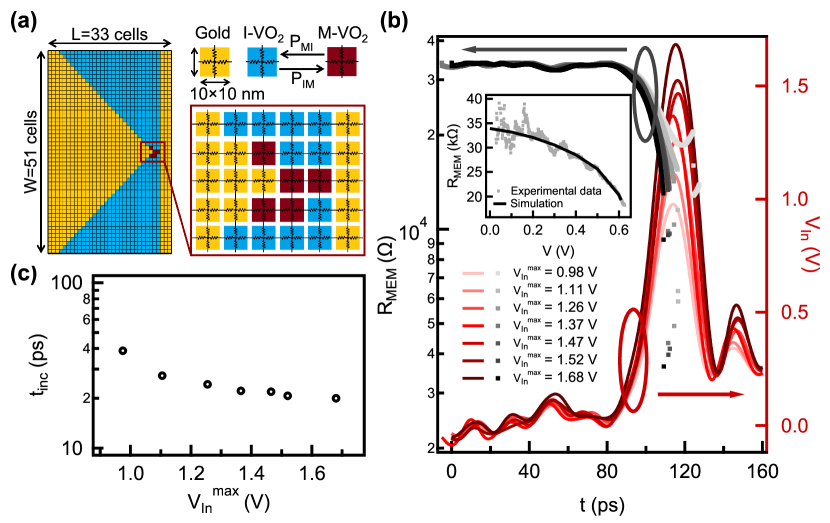
Modeling the Set Switching Dynamics. The plausibility of the set switching due to Volt-scale pulses of 20 ps FWHM within our thermally and electrically driven Mott transition picture [10] was confirmed by numerical simulations. The applied two-dimensional resistor network model [38, 39] takes into account the electrical and thermal conductivities of the VO2 layer confined by the Au electrodes. The active region is modeled as an array of 1010 nm2 cells arranged in a square lattice, as illustrated in Fig. 4(a). The state of each VO2 cell is either insulating (I-VO2, blue) or metallic (M-VO2, red) whereas the Au cells (yellow) are always in a low-resistance metallic state. The thickness of the cells is 40 nm according to the VO2 film thickness of our samples. Each cell consists of four identical resistors connecting to its nearest neighbors. All VO2 cells are initialized as I-VO2.
In our model, the phase transition of the VO2 cells is a thermally assisted process, where the and insulator-to-metal and metal-to-insulator transition probabilities depend exponentially on the temperature. The local temperature is determined from the heat equation accounting for Joule heating and heat conduction toward the neighboring cells and the substrate. Furthermore, a boundary thermal resistance was considered between the VO2 and Au cells. The resistance of an individual resistor in an I-VO2 cell depends on both the local temperature and the local electric field, whereas in the metallic state of VO2 a temperature and electric field independent resistance is assumed. The electrical and thermal material parameter values utilized by the resistor network simulation are adopted from our previous finite element simulations performed in COMSOL Multiphysics [10]. They were determined by fitting the experimental trace of the device by the simulation, as shown in the inset of Fig. 4(b). Further details on the numerical approach are provided in the Methods and Experimental Section as well as in Ref. 10.
In order to extract the incubations times according to the definition used throughout the evaluation of the measured set switching data, the experimentally realized set voltage pulses were applied to the resistor network, as shown by the red curves in Fig. 4(b). The model was solved by using ps long time steps. The gray curves in Fig. 4(b) show the time evolution of device resistance. The phase transition is hallmarked by the sudden drop of the resistance which occurs during the rise time of the set pulses, in agreement with the experiment. The simulated incubation times are exhibited in Fig. 4(c). In spite of the crude simplifications of the applied model, they fall into the ps regime, in good agreement with the experimentally observed values of 15 ps30 ps. The simulated incubation time also reveals a similar voltage dependence as its experimental counterpart, demonstrating the consistence of the measured, picosecond-scale incubation times with the electro-thermal picture of the Mott transition in VO2 nanodevices. These findings are also in agreement with the Spice simulation results of W. Yi et al. [13], where picosecond time-scale set transitions are predicted at femtojoule switching energies for active volumes comparable to our device design.
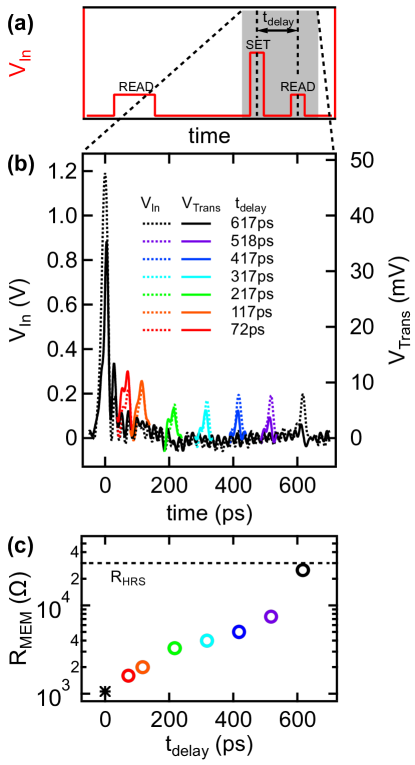
Sub-Nanosecond Reset Dynamics. Finally, we demonstrate that the HRS can be restored within 600 ps from the set voltage pulse. For this purpose, the pulsing scheme shown in Fig. 3(a) is modified by replacing the second, 1 ns long read-out pulse promptly following the set pulse by a 20 ps long, 0.2 V amplitude probe pulse. The latter is delayed by with respect to the set pulse, as illustrated in Fig. 5(a). The concept of the short probe pulse is introduced in order to minimize the impact of the readout pulse in maintaining the LRS. The initial 30 k state is confirmed by a 1 ns long, 0.25 V amplitude read-out pulse applied 100 ns before the set pulse. The 20 ps long, 1.2 V amplitude set pulse, displayed by the black dashed line at 0 ps in Fig. 5(b), switches the device into an 1 k state within the duration of the pulse, consistently with the data exhibited in Fig. 3. In the experiment shown in Fig. 5(b), identical set pulses and different times between 0 and 600 ps were utilized, as plotted by the colored (dashed lines) and (solid lines) traces. The actual device resistance is evaluated at each by fitting the response to the probe pulse according to Eq. 1 and the equivalent circuit shown in Fig. 2(d). This analysis reveals the decay of the LRS toward the HRS and evidences that the latter can be restored within 600 ps, as presented in Fig. 5(c).
Previous studies utilizing micron-scale VO2 devices concluded that the MIT is a predominantly thermal relaxation driven, slow process taking place at 10’s or even 100’s of nanoseconds [18], where the presence of long-lived metallic domains was also evidenced [19]. In contrast, our analysis unambiguously demonstrates that the relaxation to the HRS can take place at the sub-nanosecond time-scale in nanoscale VO2 cells, as shown in Fig. 5(c). This finding, together with the sub-100 ps IMT enables the orders of magnitude acceleration of VO2-based electronics, among them THz sensors [40] and oscillator circuits exploited for neuromorphic computing purposes [16].
Conclusion
In conclusion, we monitored the resistive switching dynamics in nanoscale volumes of VO2 thin films in real time at the picosecond time-scale, enabled by a special, low-capacitance electrode design. By utilizing current state of the art electronics, we demonstrated that 20 ps FWHM voltage pulses of 1.7 V amplitude trigger the insulator-metal transition with incubation times down to 15 ps, resulting in fine-tunable, analog LRS in the resistance range of 102 – 104 . These findings are supported by finite element simulations taking the combined electronic and thermal origin of the IMT into account. Our analysis of the energy consumption revealed that, depending on the targeted level, the set switching requires as little energy as 4 fJ. By applying a pump-probe pulsing scheme we demonstrated that the HRS can be restored within 600 ps. The above results represent orders of magnitude breakthroughs both in the operation frequency and energy efficiency, demonstrating the merits of nanoscale Mott devices in the electronic platforms of the Beyond-Moore Era.
Methods and Experimental Section
Device Fabrication. The VO2 layers were formed via the post-deposition heat treatment of an Al2O3/V vertical stack of 480 m Al2O3 and 100 nm V. During the heat treatment, the sample was exposed to 400 ∘C temperature and 0.1 mbar air pressure over 4.5 hours. As a result, a 40 nm thick VO2 film was created on top of a 180 nm thick V2O5 bottom layer, as confirmed by cross-sectional TEM and EELS analyses [10]. The metallic leads of 10 nm Ti and 50 nm Au were patterned by standard electron-beam lithography and deposited by electron-beam evaporation at 10-7 mbar base pressure at rates of 0.1 nm/s and 0.4 nm/s, respectively, followed by lift-off. After the completion of the CPW structure shown in Fig. 1(c), a selective etching step was carried out to remove the VO2 layer in the gap regions of the GND-S and GND-D electrodes of the CPW. During this step the sample was immersed to an acidic solution of H2O2:H3PO4:CH3COOH:HNO3 (2:16:1:1) at 50∘C for twice 5 seconds. This method yielded to 10 M parasitic resistances between the GND-S and GND-D electrodes of the CPW.
Direct Current (DC) Characterization. The schematic of the DC measurement is shown in Fig. 1(d). A slow, typically =1 Hz frequency, triangular voltage signal was applied to the device under test and the series resistor of = 0.3 – 1 k by an NI USB-6341 data acquisition unit (DAQ). The current was measured by a Femto DHPCA-100 current amplifier and recorded at the analog voltage input of the DAQ. The voltage acting on the device was determined as .
Fast Switching Setup. The schematics of the fast resistive switching setup is shown in Fig. 2(c). The device under test was contacted by two 67 GHz bandwidth Picoprobe triple probes in a vibration-damped probe station. A Micram DAC10004 100GSa/s DAC unit served as an arbitrary waveform generator (AWG) which provided voltage pulses down to 20 ps FWHM at 20 ps rise time. The output of the AWG was amplified by a Centellax UA0L65VM broadband amplifier module owing a 65 GHz analog bandwidth. The voltage pulses propagated in 0.30 m long, 70 GHz bandwidth, 50 terminated Totoku TCF280 coaxial cables. The transmitted voltage was recorded by a 50 terminated Keysight UXR1104A digital storage oscilloscope (DSO) at 256 GSa/s sampling rate and 113 GHz analog bandwidth. The input terminals of the DSO were protected by 60 GHz bandwidth RF attenuators. The signal was acquired separately by eliminating the memristor device and the probes from the circuit.
Two-Dimensional Resistor Network Simulations. The resistance of an individual resistor in the I-VO2 cell, indexed by (), depends on the local temperature and electric field and can be written as
| (2) |
where is a constant, is the band gap energy in the HRS state and is a characteristic electric field. In the LRS a temperature and electric field independent resistance value is assumed. By biasing the resistor network, the current starts to flow through the cells and the Joule heat dissipates on each resistor according . The corresponding temperature change depends on the Joule heating as well as on the heat conduction towards the nearest neighbor cells and the substrate according to
| (3) |
where is the thermal capacity of the cell, () is the thermal conductance toward the neighbor cells (substrate). The substrate is assumed to be at a base temperature. Furthermore, a boundary thermal resistance was considered between the VO2 and Au cells which determines the thermal conductance at their interface. At each time step of the simulation, the resistance of the resistor network is calculated and the electrical potential map of the resistor network is determined by a nodal analysis. Finally, is calculated via Eq. 3 and the state of each VO2 cell is updated.
The phase of a VO2 cell can change between metallic and insulating states, according to the transition probabilities given by and . These transitions are thermally activated with the transition rates of
| (4) | |||||
| (5) |
where the is an attempt rate set to unity. The potential barriers and separate the metal and insulator states. Both energy barriers have a linear temperature dependence, which vanishes at the phase transition temperature and , respectively, as
| (6) |
| (7) |
where and are constants. The electrical parameters and were deduced from the measured low-bias dependence. The thermal parameters , and were determined by fitting the high-bias trace in the insulating phase.
Author Contributions
T.N.T. and L.P. fabricated the devices. The VO2 layers were grown by G.M. M.C and Y.H. developed the fast resistive switching setup. S.W.S. and M.C. acquired and analyzed the resistive switching data. B.S. and Z.P. contributed to the lower frequency characterization of the samples. L.P. developed the two-dimensional resistor network model and performed the numerical simulations. A.H. and M.C. conceived the idea of fast resistive switching experiments and supervised the project. The manuscript was prepared by M.C., S.W.S, L.P. and A.H. All authors contributed to the discussion of the results.
Acknowledgements
This research was supported by the Ministry of Culture and Innovation and the National Research, Development and Innovation Office within the Quantum Information National Laboratory of Hungary (Grant No. 2022-2.1.1-NL-2022-00004), and the NKFI K143169 and K143282 grants. Project no. 963575 has been implemented with the support provided by the Ministry of Culture and Innovation of Hungary from the National Research, Development and Innovation Fund, financed under the KDP-2020 funding scheme. L.P. acknowledges the support of the UNKP-23-5-BME-422 new national excellence program of the Ministry for Innovation and Technology from the source of the National Research, Development and Innovation Fund and the János Bolyai Research Scholarship. J.L. and M.C. acknowledge the financial support of the Werner Siemens Stiftung.
References
- Kumar et al. [2022] S. Kumar, X. Wang, J. P. Strachan, Y. Yang, and W. D. Lu, Dynamical memristors for higher-complexity neuromorphic computing, Nature Reviews Materials 7, 575 (2022).
- Zidan et al. [2018] M. A. Zidan, J. P. Strachan, and W. D. Lu, The future of electronics based on memristive systems, Nature Electronics 1, 22 (2018).
- Li et al. [2022] Y. Li, W. Song, Z. Wang, H. Jiang, P. Yan, P. Lin, C. Li, M. Rao, M. Barnell, Q. Wu, S. Ganguli, A. K. Roy, Q. Xia, and J. J. Yang, Memristive field-programmable analog arrays for analog computing, Advanced Materials , 2206648 (2022).
- Kim et al. [2004] H.-T. Kim, B.-G. Chae, D.-H. Youn, S.-L. Maeng, G. Kim, K.-Y. Kang, and Y.-S. Lim, Mechanism and observation of mott transition in vo2-based two- and three-terminal devices, New Journal of Physics 6, 52 (2004).
- Liu et al. [2018] K. Liu, S. Lee, S. Yang, O. Delaire, and J. Wu, Recent progresses on physics and applications of vanadium dioxide, Materials Today 21, 875 (2018).
- Ko and Ramanathan [2008] C. Ko and S. Ramanathan, Observation of electric field-assisted phase transition in thin film vanadium oxide in a metal-oxide-semiconductor device geometry, Applied Physics Letters 93, 252101 (2008).
- Kim et al. [2010] J. Kim, C. Ko, A. Frenzel, S. Ramanathan, and J. E. Hoffman, Nanoscale imaging and control of resistance switching in vo2 at room temperature, Applied Physics Letters 96, 213106 (2010).
- Wu et al. [2011] B. Wu, A. Zimmers, H. Aubin, R. Ghosh, Y. Liu, and R. Lopez, Electric-field-driven phase transition in vanadium dioxide, Physical Review B 84, 241410 (2011).
- Tadjer et al. [2017] M. J. Tadjer, V. D. Wheeler, B. P. Downey, Z. R. Robinson, D. J. Meyer, C. R. Eddy, and F. J. Kub, Temperature and electric field induced metal-insulator transition in atomic layer deposited vo2 thin films, Solid-State Electronics 136, 30 (2017).
- Pósa et al. [2023] L. Pósa, P. Hornung, T. N. Török, S. W. Schmid, S. Arjmandabasi, G. Molnár, Z. Baji, G. Dražić, A. Halbritter, and J. Volk, Interplay of thermal and electronic effects in the mott transition of nanosized vo2 phase change memory devices, ACS Applied Nano Materials 6, 9137 (2023).
- Kumar et al. [2017a] S. Kumar, J. P. Strachan, and R. S. Williams, Chaotic dynamics in nanoscale nbo2 mott memristors for analogue computing, Nature 548, 318 (2017a).
- Kumar et al. [2017b] S. Kumar, Z. Wang, N. Davila, N. Kumari, K. J. Norris, X. Huang, J. P. Strachan, D. Vine, A. L. D. Kilcoyne, Y. Nishi, and R. S. Williams, Physical origins of current and temperature controlled negative differential resistances in nbo2, Nature Communications 8, 658 (2017b).
- Yi et al. [2018] W. Yi, K. K. Tsang, S. K. Lam, X. Bai, J. A. Crowell, and E. A. Flores, Biological plausibility and stochasticity in scalable vo2 active memristor neurons, Nature Communications 9, 4661 (2018).
- Corti et al. [2018] E. Corti, B. Gotsmann, K. Moselund, I. Stolichnov, A. Ionescu, and S. Karg, Resistive coupled vo2 oscillators for image recognition, in 2018 IEEE International Conference on Rebooting Computing (ICRC) (2018) pp. 1–7.
- Corti et al. [2019] E. Corti, B. Gotsmann, K. Moselund, I. Stolichnov, A. Ionescu, G. Zhong, J. Robertson, and S. Karg, Vo2 oscillators coupling for neuromorphic computation, in 2019 Joint International EUROSOI Workshop and International Conference on Ultimate Integration on Silicon (EUROSOI-ULIS) (2019) pp. 1–4.
- Corti et al. [2020] E. Corti, B. Gotsmann, K. Moselund, A. M. Ionescu, J. Robertson, and S. Karg, Scaled resistively-coupled vo2 oscillators for neuromorphic computing, Solid State Electronics 168, 107729 (2020).
- Corti et al. [2021] E. Corti, J. A. C. Jimenez, K. M. Niang, J. Robertson, K. E. Moselund, B. Gotsman, A. M. Ionescu, and S. Karg, Coupled vo2 oscillators circuit as analog first layer filter in convolutional neural networks, Frontiers in Neuroscience 15, 628254 (2021).
- del Valle et al. [2019] J. del Valle, P. Salev, F. Tesler, N. M. Vargas, Y. Kalcheim, P. Wang, J. Trastoy, M.-H. Lee, G. Kassabian, J. G. Ramírez, M. J. Rozenberg, and I. K. Schuller, Subthreshold firing in mott nanodevices, Nature 569, 388 (2019).
- Nikoo et al. [2022] M. S. Nikoo, R. Soleimanzadeh, A. Krammer, G. M. Marega, Y. Park, J. Son, A. Schueler, A. Kis, P. J. W. Moll, and E. Matioli, Electrical control of glass-like dynamics in vanadium dioxide for data storage and processing, Nature Electronics 5, 596 (2022).
- Becker et al. [1994] M. F. Becker, A. B. Buckman, R. M. Walser, T. Lépine, P. Georges, and A. Brun, Femtosecond laser excitation of the semiconductor‐metal phase transition in vo2, Applied Physics Letters 65, 1507 (1994).
- Cavalleri et al. [2001] A. Cavalleri, C. Tóth, C. W. Siders, J. A. Squier, F. Ráksi, P. Forget, and J. C. Kieffer, Femtosecond structural dynamics in vo2 during an ultrafast solid-solid phase transition, Physical Review Letters 87, 237401 (2001).
- Cavalleri et al. [2004] A. Cavalleri, T. Dekorsy, H. H. W. Chong, J. C. Kieffer, and R. W. Schoenlein, Evidence for a structurally-driven insulator-to-metal transition in vo2: A view from the ultrafast timescale, Physical Review B 70, 161102 (2004).
- Wegkamp et al. [2014] D. Wegkamp, M. Herzog, L. Xian, M. Gatti, P. Cudazzo, C. L. McGahan, R. E. Marvel, R. F. Haglund, A. Rubio, M. Wolf, and J. Stähler, Instantaneous band gap collapse in photoexcited monoclinic vo2 due to photocarrier doping, Physical Review Letters 113, 216401 (2014).
- Morrison et al. [2014] V. R. Morrison, R. P. Chatelain, K. L. Tiwari, A. Hendaoui, A. Bruhács, M. Chaker, and B. J. Siwick, A photoinduced metal-like phase of monoclinic vo2 revealed by ultrafast electron diffraction, Science 346, 445 (2014).
- Tao et al. [2014] Z. Tao, F. Zhou, T.-R. T. Han, D. Torres, T. Wang, N. Sepulveda, K. Chang, M. Young, R. R. Lunt, and C.-Y. Ruan, The nature of photoinduced phase transition and metastable states in vanadium dioxide, Scientific Reports 6, 38514 (2014).
- Liu et al. [2012] M. Liu, H. Y. Hwang, H. Tao, A. C. Strikwerda, K. Fan, G. R. Keiser, A. J. Sternbach, K. G. West, S. Kittiwatanakul, J. Lu, S. A. Wolf, F. G. Omenetto, X. Zhang, K. A. Nelson, and R. D. Averitt, Terahertz-field-induced insulator-to-metal transition in vanadium dioxide metamaterial, Nature 487, 345 (2012).
- del Valle et al. [2021] J. del Valle, N. M. Vargas, R. Rocco, P. Salev, Y. Kalcheim, P. N. Lapa, C. Adda, M.-H. Lee, P. Y. Wang, L. Fratino, M. J. Rozenberg, and I. K. Schuller, Spatiotemporal characterization of the field-induced insulator-to-metal transition, Science 373, 907 (2021).
- Pósa et al. [2021] L. Pósa, G. Molnár, B. Kalas, Z. Baji, Z. Czigány, P. Petrik, and J. Volk, A rational fabrication method for low switching-temperature vo2, Nanomaterials 11, 212 (2021).
- Csontos et al. [2023] M. Csontos, Y. Horst, N. J. Olalla, U. Koch, I. Shorubalko, A. Halbritter, and J. Leuthold, Picosecond time-scale resistive switching monitored in real-time, Advanced Electronic Materials 9, 2201104 (2023).
- Waser et al. [2009] R. Waser, R. Dittmann, G. Staikov, and K. Szot, Redox-based resistive switching memories - nanoionic mechanisms, prospects, and challenges, Advanced Materials 21, 2632 (2009).
- Gubicza et al. [2015] A. Gubicza, M. Csontos, A. Halbritter, and G. Mihály, Non-exponential resistive switching in ag2s memristors: a key to nanometer-scale non-volatile memory devices, Nanoscale 7, 4394 (2015).
- Sánta et al. [2020] B. Sánta, D. Molnár, P. Haiber, A. Gubicza, E. Szilágyi, Z. Zolnai, A. Halbritter, and M. Csontos, Nanosecond resistive switching in ag/agi/ptir nanojunctions, Beilstein Journal of Nanotechnology 11, 92 (2020).
- Cruz-Albrecht et al. [2012] J. M. Cruz-Albrecht, M. W. Yung, and N. Srinivasa, Energy-efficient neuron, synapse and stdp integrated circuits, IEEE Transactions on Biomedical Circuits and Systems 6, 246 (2012).
- Cheng et al. [2019] B. Cheng, A. Emboras, Y. Salamin, F. Ducry, P. Ma, Y. Fedoryshyn, S. Andermatt, M. Luisier, and J. Leuthold, Ultra compact electrochemical metallization cells offering reproducible atomic scale memristive switching, Communications Physics 2, 28 (2019).
- Strachan et al. [2011] J. P. Strachan, A. C. Torrezan, G. Medeiros-Ribeiro, and R. S. Williams, Measuring the switching dynamics and energy efficiency of tantalum oxide memristors, Nanotechnology 22, 505402 (2011).
- Torrezan et al. [2011] A. C. Torrezan, J. P. Strachan, G. Medeiros-Ribeiro, and R. S. Williams, Sub-nanosecond switching of a tantalum oxide memristor, Nanotechnology 22, 485203 (2011).
- Sengupta et al. [2013] B. Sengupta, A. A. Faisal, S. B. Laughlin, and J. E. Niven, The effect of cell size and channel density on neuronal information encoding and energy efficiency, Journal of Cerebral Blood Flow & Metabolism 33, 1465 (2013).
- Stoliar et al. [2013] P. Stoliar, L. Cario, E. Janod, B. Corraze, C. Guillot-Deudon, S. Salmon-Bourmand, V. Guiot, J. Tranchant, and M. Rozenberg, Universal electric-field-driven resistive transition in narrow-gap mott insulators, Advanced Materials 25, 3222 (2013).
- Rocco et al. [2022] R. Rocco, J. del Valle, H. Navarro, P. Salev, I. K. Schuller, and M. Rozenberg, Exponential escape rate of filamentary incubation in mott spiking neurons, Physical Review Applied 17, 024028 (2022).
- Qaderi et al. [2023] F. Qaderi, T. Rosca, M. Burla, J. Leuthold, D. Flandre, and A. M. Ionescu, Millimeter-wave to near-terahertz sensors based on reversible insulator-to-metal transition in vo2, Communications Materials 4, 34 (2023).