A Hybrid Delay Model for Interconnected Multi-Input Gates††thanks: This research was supported by the Austrian Science Fund (FWF) project DMAC (grant no. P32431) and the ANR DREAMY (ANR-21-CE48-0003).
Abstract
Dynamic digital timing analysis aims at substituting highly accurate but slow analog simulations of digital circuits with less accurate but fast digital approaches to facilitate tracing timing relations between individual transitions in a signal trace. This primarily requires gate delay models, where the input-to-output delay of a transition also depends on the signal history. We focus on a recently proposed hybrid delay model for CMOS multi-input gates, exemplified by a 2-input NOR gate, which is the only delay model known to us that faithfully captures both single-input switching (SIS) and multi-input switching (MIS) effects, also known as “Charlie effects”. Despite its simplicity as a first-order model, simulations have revealed that suitably parametrized versions of the model predict the actual delays of NOR gates accurately. However, the approach considers isolated gates without their interconnect.
In this work, we augment the existing model and its theoretical analysis by a first-order interconnect, and conduct a systematic evaluation of the resulting modeling accuracy: Using SPICE simulations, we study both SIS and MIS effects on the overall delay of NOR gates under variation of input driving strength, wire length, load capacitance and CMOS technology, and compare it to the predictions of appropriately parametrized versions of our model. Overall, our results reveal a surprisingly good accuracy of our fast delay model.
Index Terms:
Digital circuit, delay model, dynamic timing analysis, interconnectI Introduction
Digital timing analysis techniques are essential for modern circuit design, as they allow to validate large designs, unlike analog simulations, e.g., using SPICE. Thanks to the elaborate static timing analysis techniques available for digital timing analysis, which employ models like CCSM [1] and ECSM [2] that facilitate an accurate corner case analysis of the delays of the gates making up a digital circuit, worst-case critical path delays can be determined accurately and fast.
Still, corner-case delay estimates from static timing analysis have limitations: they consider signal transitions in isolation, in the sense that gate and interconnect delays do not take into account the history of previous transitions. By contrast, dynamic timing analysis may uncover a circuit’s behavior that becomes only visible when considering previous signal transitions when computing some transition’s delay. Two examples where this becomes central are:
-
1.
Asynchronous digital circuits. Consider the token-passing ring described and analyzed by Winstanley et al. in [3]. The circuit implements a ring oscillator made-up of stages consisting of a 2-input Muller C-gate, with its inputs connected to the previous resp. next stage. The circuit exhibits two modes of operation, namely, burst behavior versus evenly spaced output transitions, which can even switch unpredictably over time. The actual operation mode depends on the subtle interplay between two effects that determine the delay of a 2-input Muller C-gate: the drafting effect, a decrease of the delay happening when an output transition is close to the previous output transition, and the Charlie effect, (named after Charles Molnar, who identified its causes in the 70th of the last century, and nowadays known as a multiple input switching (MIS) effect [4]), an increase in the delay happening when the two inputs are switching (in the same direction) in close proximity. Consequently, to analyze the overall behavior of the ring, the timing relation of individual transitions need to be traced throughout the whole circuit.
-
2.
Spiking neural networks (SNNs). To verify the correct operation of a delay-encoded inter-neuron link design in a hardware-implemented SNN [5], the delay between successive transitions must be tracked when they travel over the link.
Analog simulations, e.g., using SPICE, are the golden standard for such dynamic timing analyses. Unfortunately, however, their simulation times are prohibitively excessive even for moderately large circuits, as the dimension of the system of differential equations that need to be solved numerically increases with the number of transistors. By constrast, digital dynamic timing analysis techniques rest on delay models that provide gate delay estimations on a per-transition basis. If explicit delay formulas are available, it allows fast correctness validation and accurate performance and power estimations [6] of a large circuit even at early stages of the development.
Delay models
The simplest non-trivial delay models that are suitable for dynamic timing analysis are single-history delay models, as defined in [7], where the input-to-output delay of a gate depends only on the previous-output-to-input delay . Particularly relevant in this context is the involution delay model (IDM) proposed in [8], which consists of zero-time gates that are interconnected by single-input single-output involution delay channels. Such channels are characterized by a delay function , which is a negative involution, in the sense that . The dependence on captures the drafting effect introduced in [3].
Unlike all other existing delay models known so far, the IDM faithfully models glitch propagation in the canonical short-pulse filtration problem [7]. Moreover, it has been shown in [9] that one can add “delay noise” to the deterministic delay function without sacrificing faithfulness. As demonstrated in some follow-up work [10], delay noise can even be used for incorporating substantial PVT variations and aging.
The IDM is also accompanied by a publicly available timing analysis framework (the Involution Tool [11]), which allows to compare the accuracy of different delay models in digital timing simulation. In particular, it allows to randomly generate input traces for a given circuit, and to evaluate the accuracy of IDM predictions compared to SPICE-generated transition times and to other digital delay models. An experimental evaluation of the modeling accuracy of the IDM in [12, 11], using both measurements and simulations, has revealed very good results for inverter chains and clock trees, albeit less so for circuits containing multi-input gates. In the case of the clock tree, a speedup of a factor of 250 has been obtained relative to SPICE in terms of simulation running times.
Models capable of capturing MIS effects have been addressed in the literature before, with approaches ranging from linear [13] fitting over higher-dimensional macromodels [14] to recent machine learning methods [15]. The resulting models are very complex, however, and definitely way beyond first-order, and thus unsuitable as a basis for fast dynamic digital timing analysis. One fairly old approach for digital dynamic timing simulation, which shares some similarities with the IDM and its multi-input gate extension [16], is IRSIM [17]. The models used there consider transistors as zero-time switches, describe the resulting system as an RC network, and discretize analog switching waveforms using a comparator. Rather than employing continuous mode switching like the IDM, however, it utilizes non-continuous mode switching. Consequently, albeit IRSIM simulation models have been reported to provide good accuracy overall, they cannot model MIS effects.
In [16], Ferdowsi et al. introduced a 4-state hybrid first-order delay model for CMOS circuits, which replaces transistors by time-varying resistors according to the Shichman-Hodges transistor model [18]. As exemplified by a CMOS 2-input NOR gate (and similar gates, including NAND and Muller C-gates), they show that the resulting model faithfully captures all MIS effects. The authors also provided an explicit procedure for model parametrization and simple analytic formulas for the delay predictions, which can be used efficiently in digital dynamic timing simulations: By means of an appropriately extended version of the Involution Tool, they also showed that appropriately parametrized versions of their model predict the actual delay of NOR gates implemented in different CMOS technologies accurately and fast.
One serious limitation of [16] is that the authors have only considered gates in isolation, i.e., without any interconnecting wires. However, wires can have a substantial effect on circuit delays in practice: they have non-negligible parasitic capacitances, resistances, and inductances, which are spatially distributed and hence change with the wire length. The first main purpose of this work is to explore the delay modeling accuracy that is achievable with an augmented version of the model of [16] that covers both the gate and the interconnect to the successor gate. Due to lack of space, we restrict our attention solely to NOR gates; since the modeling approach of [16] is applicable to other CMOS gates as well, in particular, NAND gates and Muller C-gates, however, adding an interconnect to those gates leads to similar results.
In addition, whereas it has been shown in [16] that their model considerably outperforms the IDM in terms of average modeling in the case of circuits that also contain multi-input gates, their experiments ignored the fact that combining single-history delays with MIS effects results in a delay function that depends on both and . In particular, in order to maximize the average modeling accuracy (after all, very small values of in a random trace occur rarely), their model parametrization procedure assumed . A natural question is how the prediction accuracy of a so-parametrized model behaves when both and are varied. The second main goal of the present paper is hence to conduct a refined experimental evaluation of the modeling accuracy, similar to [12], for our augmented version of the model of [16].
Detailed contributions:
-
(1)
We augment the model from [16] by an RC (L-type) interconnect and determine analytic expressions for the trajectories and the resulting delays. The choice for an L-type model as opposed to higher-order models is motivated by the goal of an analytically tractable and simple-to-compute first order model.
-
(2)
We extend the parametrization procedure from [16] to also determine the new interconnect-related model parameters. Analytic delay formulas again proved instrumental for developing a sound algorithm here.
-
(3)
We conduct a series of simulations to determine the accuracy of our augmented model for NOR gates interconnected by a wire. In our simulations, we consider two different CMOS technologies ( and ), and vary input driving strength, wire length, load capacitance, wire resistance, and wire capacitance. Using SPICE simulations, we determine for different values of and , and compare those to the predictions of an appropriately parametrized version of our generalized model (determined for ). Overall, our results reveal that the average accuracy of our model is surprisingly good (in the % range), and so is the worst-case accuracy, except for extremely small values of where is small anyway.
Paper organization: Section II provides a brief overview of the inner workings of the advanced hybrid delay model proposed in [16], and the main analytic results needed for developing the generalized model presented in Section III. In Section IV, we provide the results of the evaluation. We conclude in Section V and outline future research directions.
II Background
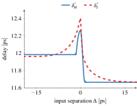
Since we generalize the first-order hybrid delay model for a CMOS NOR gate introduced in [16], we first provide an overview of its features. Consider the transistor implementation of a NOR gate in Fig. 1a. Let , , and denote the points in time when the analog trajectories of input signals , , and the output signal cross the discretization threshold voltage , respectively. Varying and allows to study the gate delay ( resp. , depending on the particular output state) over the relative input separation time .


| Mode | |||||
|---|---|---|---|---|---|
The advanced hybrid delay model proposed in [16] is a generalization of the simple model introduced in [19]. Informally speaking, it replaces the immediate switching-on of the resistance of the pMOS transistors (see Fig. 1a) by the time evolution function representing the Shichman-Hodges transistor model [18], which is given by
| (1) |
Herein, [] and on-resistance [] are constant slope parameters of the transistor ; represents the time when the respective transistor is switched on. Crucial in this model is that since the switching-on of the nMOS transistors is supposed to happen instantaneously, .
Applying Kirchhoff’s rules to Fig. 1b leads to which can be transformed into the non-homogeneous non-autonomous first-order ODE with non-constant coefficients
| (2) |
where and and using the notation , , , , and for the two nMOS transistors and . It is well-known that the general solution of (2) is
| (3) |
where denotes the initial condition and . As comprehensively described in [16], depending on each particular resistor’s mode in each input state transition, different expressions for and are obtained. Denoting , , and , Table I summarizes them.
In order to prove that the resulting hybrid model faithfully captures all MIS effects, the authors derived analytic expressions for the trajectories of for every mode switch , and then determined the MIS delays for arbitrary by the following procedure:
-
•
Compute , and use it as the initial value for obtaining ; the sought gate delay is the time until the latter crosses the threshold voltage .
-
•
Compute , and use it as the initial value for obtaining ; the sought gate delay is the time until the latter crosses the threshold voltage .
Due to some symmetry, it turned out to be sufficient to derive analytic expressions for the case only: the corresponding formulas for can be obtained from those by exchanging and as well as and , respectively.
Inverting the resulting trajectory formulas finally provided analytic formulas for the gate delay as functions of and the initial state, which are given in the following Theorem 1. In the proof of this theorem in [16], the range of had to be split into 4 cases; an additional free parameter (for some suitably chosen ) was required to smoothly paste the different ranges.
Theorem 1 ([16, Thm. 2]).
Let and be the given initial states of respectively and . Then, for any , the extended delay functions for falling and rising output transitions of our model are
where and Case w.r.t.
-
•
Case 1: ,
-
•
Case 2: ,
-
•
Case 3: ,
-
•
Case 4: .
Herein,
and
and can be easily obtained by our symmetry.
The delay formulas provided by Theorem 1 capture both multi input switching (MIS) and single input switching (SIS). For the SIS switching , for example, it suffices to replace the initial value in by the initial value , which gives the output voltage at the time the previous switch from to . For verifying the MIS effects, it even suffices to start with the initial values resp. in the case of falling resp. rising input transitions, which represent the situation where the NOR gate has been initialized to the state resp. long ago.
In [16], the authors showed how to parametrize their hybrid model for matching a given circuit, and demonstrated a very good modeling accuracy for both and CMOS technologies by comparing the delay predictions of the hybrid model with SPICE-generated actual circuit delays .
III Adding Interconnect Modeling
Since the model of [16] considers a single NOR gate in isolation, the question arises whether and how much the delay modeling accuracy suffers when considering gates and interconnecting together. Indeed, wires can have a substantial effect on circuit delays: Actual wires have parasitic capacitances, resistances, and inductances, which are spatially distributed and hence change with the wire length. State-of-the-art interconnect modeling usually breaks up wires into segments, each of which is characterized by some lumped model, typically of , T, and RC type [20].
Since our focus is on exploring the modeling accuracy achievable with first-order hybrid models, we restrict our attention to the lumped RC model, as shown in Fig. 2. Although this model is known to be less accurate than e.g. the model in static timing analysis, it is the only one that can be added to the gate model of [16] without turning it into a second-order model: Adding a T or model would add another state-holding stage (capacitor) and hence raise the dimension of the ODE systems to 2.

III-A The interconnect-augmented hybrid delay model
Applying Kirchhoff’s rules to the interconnect-augmented variable resistor model easily lead to the non-homogeneous ODE
which is just 2 with the additional factor in all terms except . Since this non-constant factor makes the already very challenging derivations leading to the analytic delay expressions given in Theorem 1 even worse, if at all tractable, we decided to take the “easy route” of approximating by a constant value: A constant value for enables us to efficiently solve the above ODE, by just replacing with in 2. In order to reduce the approximation error, however, we use different values of in different scenarios. Note that this “easy route” also works for augmenting delay models for other gates, including Muller C-gates.
Recall that in the original hybrid model, each mode switch enables some specific ODE system, the solution of which gives the respective trajectory. Fortunately, as can be observed in Table I, all transitions except and lead to a constant value for a priori. Consequently, for those six transitions, we can safely substitute by the appropriate constant value.
Unfortunately, this is not the case for the transitions and , though, so replacing by some constant value introduces some approximation error. Fortunately, the time span during which varies significantly is very small. Moreover, its variability is not very large either: In particular, as the switch-on of a transistor is fast, one may reasonably conjecture that replacing by should lead to a good approximation; and indeed, the results of our validation experiments in Section IV confirm this conjecture. One can infer from Table I that resp. leads to resp. , which both lead to . Putting everything together, Table II summarizes all exact and approximate values of and corresponding to each mode switch.
| MS | ||||
|---|---|---|---|---|
The results of the above discussion are summarized in the following 1, which gives the delay predictions of our generalized advanced model for the case . As in the case of Theorem 1, the analogous expressions for and can be obtained by exchanging and as well as and , respectively.
Corollary 1.
Let and be the given initial states of respectively and . Then, for any , the delay functions for falling and rising output transitions of our model are
where , , , and . Besides, , and for are as defined in Theorem 1.
A mandatory prerequisite for using our generalized model and, in particular, for conducting the validation experiments in Section IV, is a parametrization procedure that allows to determine suitable model parameters. It will be developed in Section III-B. Given the additional parameter (), the procedure is considerably more involved than the one used for the original model in [16].
III-B Parametrization procedure
Recall the model’s primary objective, which is capturing the MIS effects as well as possible. As in [16], our parametrization procedure aims at matching the characteristic Charlie delay values , , and the values , , and of a real circuit by the corresponding predicted delay values of our model given in 1 as closely as possible.
Whereas just applying the least square fitting approach advocated in [16] seemed appropriate at the first glance, it turned out that the additional term considerably changed the situation. To be more precise, assuming that the on-resistors of the two nMOS transistors and are roughly be the same, it turns out that . In the case of , which represents the original model, this translates to . In [16], this was ensured by choosing a suitable pure delay , also present in the original IDM, which defers the switching to the new state upon an input transition. This way, could be enforced.
In the case of , we have this resistor as another handle on matching a given ratio , besides . Any setting of these parameters that satisfies
| (4) |
is a feasible choice here.
Indeed, contrary to our initial conjecture that the additional term might make the parametrization of the generalized model more difficult than the parametrization of the original model, it turned out that the relation implied by 4 enabled us to completely decouple the parametrization process for the falling and rising output transition cases. We therefore arrived at the parametrization procedure shown in Algorithm 1, where the outer loop searches for the best value of within some a priori given range .
IV Evaluation of accuracy
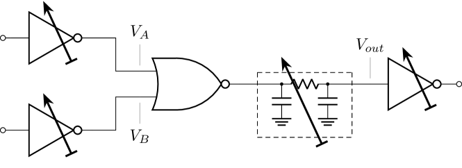
We conducted simulations to evaluate the prediction accuracy of our generalized model. As illustrated in Fig. 3, we instantiated a NOR gate connected to an inverter, acting as its load, via a controlled wire. The inputs of the NOR gate are driven by a chain of 4 inverters acting as signal shaping gates. The chain input is stimulated by a saturated ramp with a rise/fall time of 0.1 fs, which leads to “natural” signal waveforms at the chain output.
For every setting, the following steps were performed:
-
(1)
Based on a Verilog description of our CMOS NOR gate implementation, we used the Cadence tools Genus and Innovus (version 19.11) for placing and routing our design.
-
(2)
Using the extracted parasitic networks from the final layout, we performed SPICE simulations to determine for different values of and .
-
(3)
Using the measured delay values , , and as well as , , and obtained for and an estimate111Actually, the parametrization procedure can adapt to a large range of values for , by scaling the resistors , and appropriately. of the lumped load capacitance , we used Algorithm 1 for finding a suitable parametrization of our model.
-
(4)
Using the equations given in 1, we computed the predictions of the parametrized model for different values of and , and compared the outcome to the measured delays.
The different settings used in the evaluation range from different implementation technologies to varying driving strengths and load capacitances to different wire lengths, wire resistances, and wire capacitances. A representative sample of our results will be presented in the following subsections. Most of them have been obtained for a CMOS NOR gate from the Nangate Open Cell Library featuring FreePDK15 FinFET models [21] (). Qualitatively similar results have been obtained for the UMC technology with supply voltage.
Overall, the accuracy of our generalized model is good. This is in stark contrast to the original model [16], however, where it turned out that even the parametrization procedure in step (3) already failed in most scenarios. This confirms that adding is really instrumental for modeling interconnected gates.
IV-A MIS accuracy
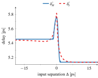
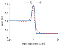
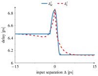
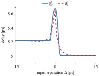
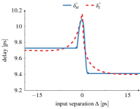
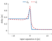
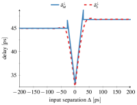
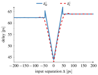
IV-A1 Wire length
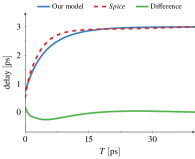
Using the 15 nm technology, we varied the length of the wire driven by the NOR gate between and (in micrometer222Note that is actually the parameter $LENGTH in the command relativePlace inv1 nor1 -relation R -xOffset $LENGTH -yOffset 0 and hence almost (i.e., besides vias) the length in m.), i.e., within a factor of 5. The dashed red curves in Fig. 4 show the resulting delays for and varying ; the case will be considered in Section IV-B. The blue curve in Fig. 4 depicts the delay predictions of the model parametrized according to Table III, which match the real delays well.
| Parameters for | ||||
| Parameters for | ||||
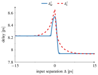
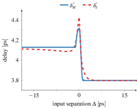
IV-A2 Wire resistance and capacitance
In order to verify the ability of our model to adapt to varying parasitic networks, we artificially changed the resistances and capacitances of the extracted network for wire length : In one setting, we halved all the resistor values, in another setting, we doubled the values of all capacitors. Fig. 5 shows both the real delays (dashed red curves) and the predictions of our model (blue curves) parametrized according to Table IV.
| Parameters for doubling the capacitances | ||||
| Parameters for half the resistor values | ||||
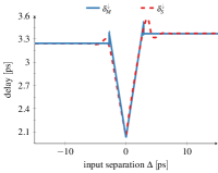
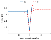
IV-A3 Input gate driving strength
In two other settings, we varied the driving strength of the two input inverters in Fig. 3 that drive and of the NOR gate driving a wire with length . More specifically, we used both a strong input inverter (with four parallel pMOS and nMOS transistors) and a weak input inverter, which was simulated by letting the input inverters drive three more NOR gates, which resulted in a fan-out of four. Fig. 6 shows the results for both cases, which have been obtained using the model parameters given in Table V.
| Parameters for weak input | ||||
| Parameters for strong input | ||||
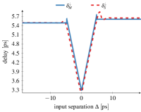
IV-A4 Load capacitance
We also varied the load capacitance of the NOR gate with wire lengths and , by increasing its fan-out: We replaced the single inverter used in the previous settings by inverters that consist of , and parallel pMOS and nMOS transistors. Fig. 7 shows the results, using the parametrization given in Table VI.
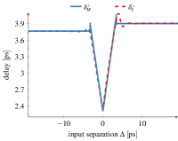
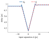
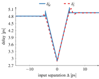
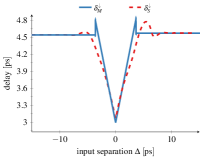
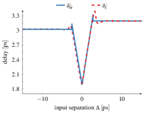
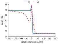
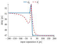
IV-B SIS accuracy
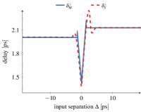
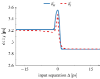
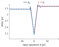
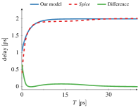
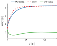
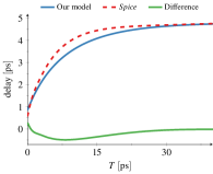
Up to now, we have exclusively focused on evaluating the modeling accuracy w.r.t. varying for the case . Since the model parametrization is exclusively based on this choice of delay values, it is essential to also also assess the accuracy of the resulting model’s predictions for the case of small previous-output-to-input delays . In this subsection, we will hence vary while choosing , which is equivalent to the SIS case.
Fig. 8a, Fig. 8b, Fig. 8c, and Fig. 8d compare the real gate delays (dashed red curve) and the delays predicted by our model (blue curve) as a function of , for different wire lengths, wire capacitances and input driving strengths. The green curve depicts the absolute prediction error.
Whereas the perfect matching between the real delays and the model prediction for is not surprising, given that the parametrization procedure relies on the delay values for , the reasonably small prediction error for small values of is remarkable. Significant errors occur only for extremely small values of , in particular, for short wires (), where the circuit delay is extremely small anyway.
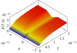
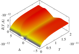
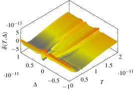
IV-C Delay accuracy in terms of both and
Whereas the cases resp. considered in the two previous subsections are arguably the most relevant ones for typical signal traces, it is also important to study the delay prediction accuracy for arbitrary values of and . To this end, Fig. 9 provides the appropriate 3D diagrams for the NOR with wire length : Fig. 9a shows the delay obtained by our model, Fig. 9b provides the results from SPICE simulations, and Fig. 9c shows the difference. It is apparent that the model’s inaccuracy increases substantially only (i) in the region where gets close to 0, for any value of , and (ii) in the two “dipped” regions in direction, for some value of close to 0. Indeed, (i) is confirmed by Fig. 8b, which reveals a notable relative error already for ps for . Similarly, Fig. 4c shows that the model predictions do not perfectly match the “oscillating” real delays in the range ps, for example. The worst-case absolute error in these regions is ps, which occurs for a very small value of where the real circuit delay is as low as ps. The overall root-mean-square absolute error is only ps.
Accordingly, the worst-case relative error is up to %, which is small given the small circuit delays in the region close to where such errors occur. Overall, the RMS relative error is %, which is primarily caused by the moderately large error throughout region (i). Outside of these regions (i) and (ii), however, the achieved accuracy is indeed surprisingly small for a first-order model like ours.
| Parameters for | ||||
| Parameters for | ||||
IV-D Other technologies
To validate that our model achieves comparable modeling accuracies also in different technologies, we re-run simulations also for a NOR gate in UMC technology with . Since the results are qualitatively similar, we will present only a small subset of those in this paper. Fig. 10 shows the results for two different wire lengths , using the parameters given in Table VII.
V Conclusions
We generalized a recently proposed hybrid delay model for a 2-input NOR gate to accurately predict both SIS and MIS delays in the presence of interconnecting wires. We demonstrated its surprising modeling accuracy by means of simulations performed in a wide range of different settings: varying wire lengths, resistances/capacitances, input driving strengths, output load capacitances, and two different CMOS technologies. Part of our current/future work is devoted to applying our modeling approach to larger circuits.
References
- [1] CCS Timing Library Characterization Guidelines, Synopsis Inc., October 2016, version 3.4.
- [2] Effective Current Source Model (ECSM) Timing and Power Specification, Cadence Design Systems, January 2015, version 2.1.2.
- [3] A. J. Winstanley, A. Garivier, and M. R. Greenstreet, “An Event Spacing Experiment,” in Proc. ASYNC, April 2002, pp. 47–56.
- [4] L.-C. Chen, S. K. Gupta, and M. A. Breuer, “A new gate delay model for simultaneous switching and its applications,” in Proc. of the 38th Design Automation Conference, 2001, pp. 289–294.
- [5] M. Bouvier, A. Valentian, T. Mesquida, F. Rummens, M. Reyboz, E. Vianello, and E. Beigne, “Spiking neural networks hardware implementations and challenges: A survey,” J. Emerg. Technol. Comput. Syst., vol. 15, no. 2, apr 2019.
- [6] F. N. Najm, “A survey of power estimation techniques in vlsi circuits,” IEEE Transactions on Very Large Scale Integration (VLSI) Systems, vol. 2, no. 4, pp. 446–455, 1994.
- [7] M. Függer, T. Nowak, and U. Schmid, “Unfaithful glitch propagation in existing binary circuit models,” IEEE Transactions on Computers, vol. 65, no. 3, pp. 964–978, March 2016.
- [8] M. Függer, R. Najvirt, T. Nowak, and U. Schmid, “A faithful binary circuit model,” IEEE Transactions on Computer-Aided Design of Integrated Circuits and Systems, vol. 39, no. 10, pp. 2784–2797, 2020.
- [9] M. Függer, J. Maier, R. Najvirt, T. Nowak, and U. Schmid, “A faithful binary circuit model with adversarial noise,” in Proc. DATE, March 2018, pp. 1327–1332.
- [10] D. Öhlinger and U. Schmid, “A digital delay model supporting large adversarial delay variations,” 2023, (to appear at DDECS’23).
- [11] D. Öhlinger, J. Maier, M. Függer, and U. Schmid, “The involution tool for accurate digital timing and power analysis,” Integration, vol. 76, pp. 87 – 98, 2021.
- [12] R. Najvirt, U. Schmid, M. Hofbauer, M. Függer, T. Nowak, and K. Schweiger, “Experimental validation of a faithful binary circuit model,” in Proc. GLSVLSI, 2015, pp. 355–360.
- [13] A. R. Subramaniam, J. Roveda, and Y. Cao, “A finite-point method for efficient gate characterization under multiple input switching,” ACM Trans. Des. Autom. Electron. Syst., vol. 21, no. 1, pp. 10:1–10:25, Dec. 2015. [Online]. Available: http://doi.acm.org/10.1145/2778970
- [14] V. Chandramouli and K. A. Sakallah, “Modeling the effects of temporal proximity of input transitions on gate propagation delay and transition time,” in Proc. DAC, 1996, p. 617–622.
- [15] O. V. S. Shashank Ram and S. Saurabh, “Modeling multiple-input switching in timing analysis using machine learning,” IEEE Transactions on Computer-Aided Design of Integrated Circuits and Systems, vol. 40, no. 4, pp. 723–734, 2021.
- [16] A. Ferdowsi, U. Schmid, and J. Salzmann, “An accurate hybrid delay model for multi-input gates,” arXiv preprint arXiv:2211.10628, 2022, (to appear in ICCAD’23).
- [17] A. Salz and M. Horowitz, “Irsim: An incremental mos switch-level simulator,” in Proc. DAC, 1989, pp. 173–178.
- [18] H. Shichman and D. A. Hodges, “Modeling and simulation of insulated-gate field-effect transistor switching circuits,” IEEE Journal of Solid-State Circuits, vol. 3, no. 3, pp. 285–289, Sep. 1968.
- [19] A. Ferdowsi, J. Maier, D. Öhlinger, and U. Schmid, “A simple hybrid model for accurate delay modeling of a multi-input gate,” in Proc. DATE, 2022, pp. 1461–1466.
- [20] M. R. Jan, C. Anantha, N. Borivoje et al., “Digital integrated circuits: a design perspective,” Pearson, 2003.
- [21] M. Martins, J. M. Matos, R. P. Ribas, A. Reis, G. Schlinker, L. Rech, and J. Michelsen, “Open cell library in 15nm freepdk technology,” in Proc. ISPD, 2015, pp. 171–178.