Effective medium theory for the electrical conductance of random resistor networks which mimic crack-template-based transparent conductive films
Abstract
We studied random resistor networks produced with regular structure and random distribution of edge conductances. These networks are intended to mimic crack-template-based transparent conductive films as well some random networks produced using nano-imprinting technology. Applying an effective medium theory, we found out that the electrical conductance of such networks is proportional to the square root of the number density of conductive edges. This dependence is in agreement with numerical calculations in Voronoi networks, although the effective conductances are larger.
Transparent conductive films (TCFs) also denoted as transparent conductive electrodes (TCEs) are widely used for creating displays and touch screens [1], transparent heaters [2, 3], solar cells [4, 5, 6, 7, 8], electromagnetic interference (EMI) shields [9, 10, 11], thermochromic devices [12], etc. Widespread devices based on oxides, e.g., zinc oxide (ZnO), indium tin oxide (ITO), etc., have a number of significant disadvantages [1]. For example, there are high material costs of ITO-based TCFs, indium deficiency, damage to organic substrates during sputtering, and fragility; an important disadvantage for their application in solar cells is the strong absorption of ITO in the UV and blue spectral ranges [13]; brittleness is a serious obstacle to the use of such transparent electrodes for flexible and stretchable electronics [14, 15, 16, 17, 18]. The listed disadvantages lead to the search for new approaches, for example, the development of printing technologies [19, 20, 21] and the creation of transparent electrodes based on templates, including natural templates and crack templates [22, 23, 24, 25].
Despite significant advances in the technology for the production of a variety of TCFs, there remain many technological and theoretical problems that are pending. In the case of TCFs based on carbon nanotubes (CNTs) and metallic nanowires (NWs), the concentration of conducting particles must be large enough to ensure the appearance of a conducting network connecting the opposite boundaries of the film, i.e., the system must be above the percolation threshold. At the same time, the concentration should be low enough to ensure high transparency of the film. These demands are conflicting.
In the case of nanowire-based TCFs [26], overheated areas (hot spots) may appear, which lead to degradation of the conductive films, which is a serious problem [27, 28, 29, 30, 31, 32]. Heat uniformity is a key requirement in the case of transparent heaters [33, 3]. Moreover, in the case of nanowire-based TCFs, there are dead ends of the nanowires which do not contribute to the electrical conductance, while decreases the transparency of TCFs [34]. The electrical resistance of junctions between nanowires contribute significantly to the resistance of the such TCFs [35, 36, 37]. To ensure high-quality contacts between nanowires and reduce the junction resistance, various processing methods are used (see, e.g, Ref. 38 with a review of technologies for welding silver nanowires). Using these technologies, depending on the initial resistance, the sheet resistance can be reduced by several orders of magnitude to tens of ohms. So-called seamless or junction-free networks are more or less free of above issues as hot spots, dead ends and junction resistance.
Uniform illumination is crucial for ensuring the imaging quality when TCFs are used for EMI shielding in the optical imaging domain. As compared to regular periodic networks (square, honeycomb), the stray light energy from high-order diffractions by the random network is significantly less [39, 40], which indicates the good optical performance of such random networks [41, 9, 42, 43, 44, 39]. Moreover, random metal networks produce neither moiré nor starburst patterns unlike networks with periodical structure [45, 46, 47].
Seamless random metallic networks produced using crack templates seem to be a very promising kind of TCFs since inhomogeneity, dead ends and hot spots are less likely, while technologies are well elaborated [48, 11]. To mimic crack templates, Voronoi tessellation (also known as Thiessen polygons) is used [49, 50, 51, 52, 53]. Moreover, Thiessen-polygon metal meshes can be directly fabricated through nano-imprinting technology [44].
Kumar and Kulkarni [34] proposed a formula describing the sheet resistance of random resistor network on main physical parameters, viz,
| (1) |
where is the resistivity of the material, and are the width and the thickness of the rectangular wire, respectively, and is the number of wire segments per unit area. Although the authors considered their method as purely geometrical, in fact, this is a kind of mean-field approach (MFA). In the case of random resistor networks, the MFA deals with only one conductor placed in the mean electric field that all other conductors produce, instead of considering of all the conductors in a system. The method is based on the fact that in a dense, homogeneous and isotropic two-dimensional RRN, the electric potential is expected to change linearly between two electrodes applied to opposite boundaries of such an RRN. Kumar and Kulkarni [34] supposed that when a potential difference is applied to the opposite border of a sample, the number of conductive wires intersecting an equipotential line is supposed to be per unit length. Recently, Tarasevich, Eserkepov, and Vodolazskaya [51] demonstrated that this assumption overestimates the intersection number by about 1.5 times. More exact formula based on a MFA
| (2) |
additionally includes the mean length of conductive wires, [51]. Although (2) agrees better with the results of direct calculations of electrical conductance than (1), both formulas overestimate the electrical conductivity.
However, the effective medium theory (EMT) [54] is often applied to predict physical properties, e.g., electrical conductance, of random systems including random resistor networks [55, 56, 57, 58]. The goal of the present work is an investigation of the electrical properties of artificial computer-generated networks that are intended to mimic the properties of real-world crack-template-based TCFs, viz, we intend to obtain a dependence of the electrical conductance of networks under consideration on main physical parameters.
Results of image processing of published photos of crack-template-based TCFs evidenced that, in crack patterns, the typical value of the node valence is 3 [51]. A small amount of nodes owning valence 1 corresponds to dead ends, their incident edges do not contribute to the electrical conductivity. Besides, boundaries of photos produce fictional nodes with valence 1, these fictional nodes correspond none real nodes. A small amount of nodes owning valence 2, in fact, correspond to bents on wires. A small amount of nodes owning valence greater than 3 should be treated as an artifact of image processing of photos with modest resolution, when two or more nodes are treated as only one node, since simplest mechanical arguments suggest that X-shaped cracks are highly unlikely. Thus, networks with valence 3 can be used to mimic crack-template-based TCFs.
A Voronoi tessellation is a partition of a space into regions close with respect to the Euclidean distance to each of a given set of objects (see, e.g., [59]). In our study, we deal with random plane Voronoi diagrams. In this particular case, points (seeds) are randomly distributed within a bounded domain on a plane. In a random plane Voronoi diagram, the degree of each vertex is 3, while the average number of vertices in a cell is 6 [60]. Thus, from the point of view of the graph theory, a random plane Voronoi tessellation generates a 3-regular planar graph. Since crack patterns demonstrate the similar property, random plane Voronoi diagram seems to be a reasonable and useful mathematical model of crack patterns [49, 50, 51, 52, 53]. However, even simpler 3-regular network seems to be appropriate for a preliminarily evaluation of the electrical conductivity of crack-template-based TCFs, i.e., a hexagonal network in which each edge posses a random electrical resistance drawn from an appropriate distribution. Since the electrical resistance of a wire is proportional to its length, the ‘appropriate distribution’ in this context means ‘the edge length distribution of random plane Voronoi diagram’.
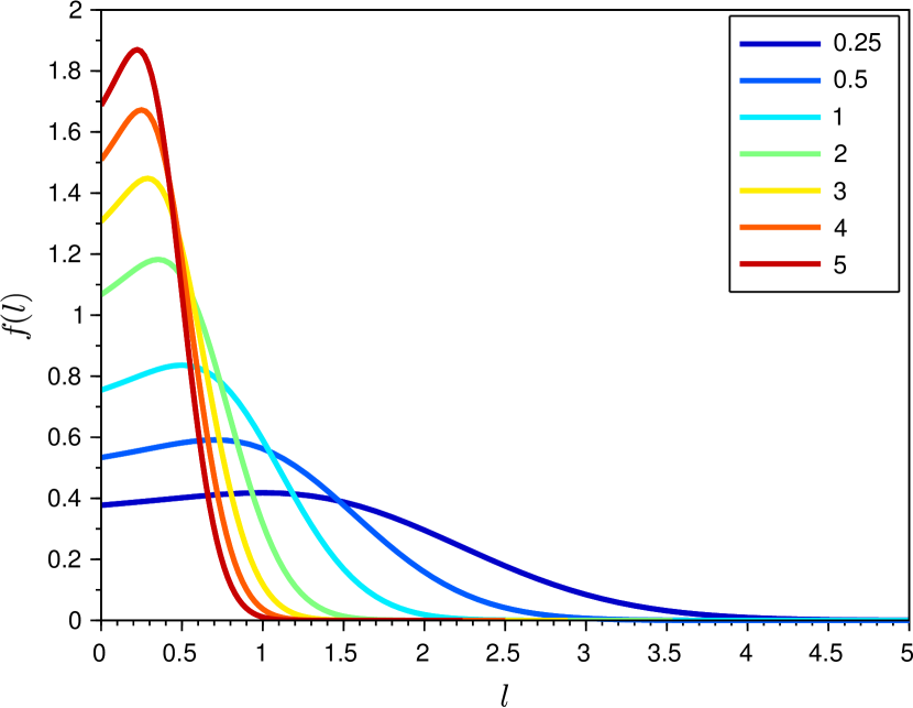
Thus, in our study, we use a hexagonal network, the edges of which have random electrical resistances. The probability density function (PDF) of these random resistances corresponds to the PDF of edge lengths in a random plane Voronoi network. We used a rectangular domain , where , while . When the side of the regular hexagon is , the number density of hexagons, i.e., the seed concentration is . For a random plane Voronoi tessellation, the PDF of the edge lengths is known in quadratures [61, 62], the PDF for the unit seed density was calculated [62]. For an arbitrary seed density, the PDF can be rescaled as follows. Let the seed density be equal to , then the new PDF can be obtained from the initial one by replacing and (Fig. 1).
When the edge length has a PDF , the PDF of the electrical conductance can be found, taking into account that the electrical conductance depends on the length of the conductor , i.e., , namely, the electrical conductance is inversely proportional to the length of the conductor (edge)
| (3) |
Then (see, e.g., [63]), Here, is the inverse function of : .
| (4) |
| (5) |
| (6) |
To calculate the electrical conductance, we attached a pair of superconducting buses to the two opposite boundaries of the domain in such a way that the potential difference was applied either along axis or along axis . Applying Ohm’s law to each resistor (hexagon edge) and Kirchhoff’s point rule to each junction (vertex of the honeycomb lattice), a system of linear equations was obtained. Such an This system was solved numerically. Since , the resistances along and axes are different. The effective conductivity, , can be calculated as follows.
| (7) |
For each value of the seed concentration, the effective conductivity was averaged over 100 independent runs and both directions. The the standard deviations of the mean are of the order of the marker size.
The main ideas of applying the EMT to networks with a regular structure and various conductances of edges are presented in the works [64, 55, 65, 66, 56]. Alternatively, a more formal and general consideration based on Foster’s theorem [67] is possible [68]. Kirkpatrick [64, 55] considered a random electrical network constructed from a hypercubic lattice in any dimension (square for , cubic for , etc.). Lattice edges were treated as circuit elements with (possibly complex) independent random conductances drawn from a general probability distribution. The EMT offers a way to replace a random network with a uniform one, where all edges have the same conductance [55]. When a voltage is applied along one axis of a random resistor network, the distribution of potentials in this network may be regarded as a superposition of an homogeneous ‘external field’ and a fluctuating ‘local field’, whose average value over any sufficiently large region has to be zero. When the values of the edge conductances are drawn from the probability distribution (which can be either continuous or discrete), the requirement that the mean value of the ‘local field’ be equal to zero gives the condition that determines the effective conductance
| (8) |
where is the valence of nodes in the lattice ( for , for , etc.)
Following [66], we start with an infinite hexagonal network (honeycomb), in which conductance of each edge is . The conductance between the two nearest nodes and of this network (Fig. 2a) can be found as follows. Let current be injected into node . Due to the symmetry of the system, the current in each of the three edges incident on node will be equal to (Fig. 2b). Let current be removed from node . Due to the symmetry of the system, the current in each of the three edges incident on node will be equal to (Fig. 2c). Then, by virtue of the superposition principle, the total current in the edge is equal to .
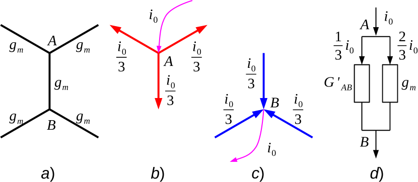
The conductance of the network between nodes and is equal to the sum of the conductance of edge () and the conductance of the entire network when edge is removed () (Fig. 2d)
| (9) |
Since the current through conductance is twice as large as the current through conductance , then . This value is consistent with the general formula for random regular networks [68]. Hence,
| (10) |
In the case of a uniform network, for any node the following equality holds:
| (11) |
Here, the summation is carried out over the nodes adjacent to node . Although the derivation of the two-point resistance was based on the homogeneity of the system, any continuous deformation of the system under consideration cannot affect the electrical conductivity, i.e., the result has to be valid for any system which topologically equivalent to the honeycomb network, in other words, for any planar 3-regular graph (network). This statement is consistent with the results by Marchant [68].
Now we replace one of the conductances with the conductance (Fig. 3a).
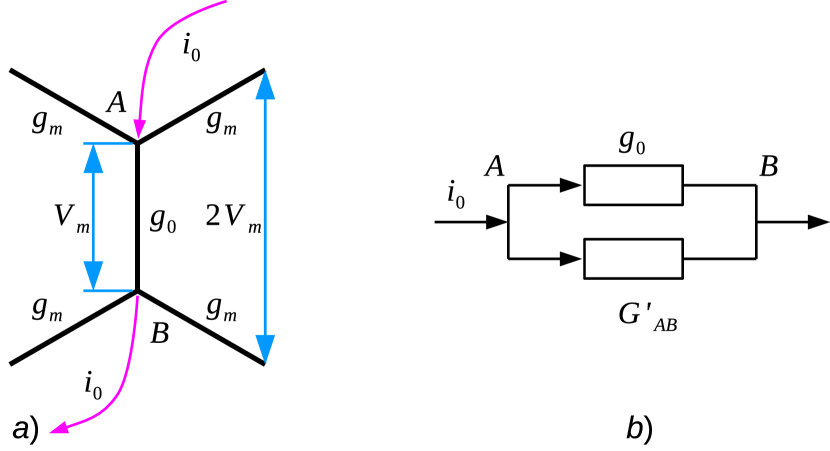
When one conductance is replaced, the solution can be constructed according to the principle of superposition, that is, to the solution for a uniform field in which the voltages increase by a constant value in each line, we have to add the influence of a fictitious current flowing into node and flowing out from node ,
| (12) |
The first term of (12) corresponds to the two currents flowing through two conductances into node , while the second one corresponds to the current flowing out of this node via conductance . Then,
| (13) |
This current creates an additional voltage between nodes and , which can be found using Fig. 3b.
| (14) |
Taking into account the previously found value for
| (15) |
Accounting for (13), we have
| (16) |
Let the conductance values of the edges in a random network obey to the PDF , then the conductance of the effective uniform network can be found from the requirement that the mean value of has to be equal to zero
| (17) |
Equation (17) can be solved numerically. For this purpose it can be rewritten in a form convenient for iterations (see Appendix A)
| (18) |
Numerical solution of (18) leads to the values of the effective electrical conductance presented in Table 1. To check the accuracy, the average value of potential fluctuation, , is presented. is the cell edge length of a regular hexagonal network with cell density ; is the conductivity per unit length, is the electrical conductance of a honeycomb network with edge conductance .
| 0.01 | 0.173 | 0.176 | 1.85 | 6.204 | 0.0283 | 0.1014 |
| 0.25 | 0.866 | 0.878 | 1.86 | 1.241 | 0.7075 | 0.5068 |
| 0.64 | 1.386 | 1.405 | 1.85 | 0.776 | 1.8111 | 0.8109 |
| 1.0 | 1.732 | 1.756 | 1.85 | 0.620 | 2.8298 | 1.0136 |
| 2.0 | 2.449 | 2.483 | 1.85 | 0.439 | 5.6596 | 1.4335 |
| 3.0 | 3.000 | 3.041 | 1.85 | 0.358 | 8.4894 | 1.7556 |
| 4.0 | 3.464 | 3.511 | 1.85 | 0.310 | 11.319 | 2.0272 |
| 5.00 | 3.873 | 3.926 | 1.85 | 0.277 | 14.149 | 2.2665 |
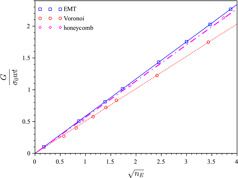
Figure 4 shows a comparison of the results of direct computations of the electrical conductance of the random Voronoi network with the predictions of the EMT. The EMT predicts a linear dependence of the electrical conductance on the square root of the edge concentration (solid line in Fig. 4), but slightly overestimates the electrical conductance as compared to direct calculations, which give a slope of [53] (dotted line), i.e., the EMT predicts the value of slope about 15% larger as compared to direct computations. The EMT is slightly worse as compared to the mean field method (slope ) [53].
It should be kept in mind that the Voronoi diagram is not a perfect hexagonal network, viz, its cells have 6 nodes only in average. To estimate the effect of network imperfection, we computed the electrical conductances of hexagonal networks in which the resistivities of edges correspond to the PDF of edge length in random Voronoi diagrams [62]. In this case the slope is 0.5686 (dash-dot line). This small deviation of the EMT prediction and the direct computation is not surprising, since Marchant [68] have explained the nature of the error inherent in the application of EMT to regular networks. Namely, replacement of the distribution of edge conductivities by a unique value found in the ‘effective network’ introduces an error that grows with the broadening of the real distribution of conductivities; i.e., the broader the PDF the larger the error.
Following [49, 50, 51, 52, 53], we mimic crack-template-based transparent conductive films, using the random resistor networks. In our study, this random resistor network corresponded to a hexagonal network with random conductivities of edges. To estimate the dependence of the electrical conductance of such transparent conductive films on main physical parameters, we utilised the effective medium theory in the same manner as [64, 55, 65, 66]. For random hexagonal networks, the effective medium theory provides a nice approximation of the dependency of the electrical conductivity on the number density of edges. We found that the electrical conductance is proportional to . Comparison of the effective medium theory predictions with direct computations of the dependency of the electrical conductance on the number density of edges in the random plane Voronoi tessellation, suggests that not only valence of vertices preordains the main behavior of the network conductance. However, even an advanced consideration [68] based on Foster’s theorem [67] can hardly improve the prediction significantly.
*
Appendix A Transformation of the equation for the electrical conductance of the effective medium to a form suitable for iteration
Consider (17). Since can be presented as , then
| (19) |
Hence, (17) can be rewritten as follows
| (20) |
According to definition of a PDF, hence,
| (21) |
Equation
| (22) |
is suitable to find iteratively
| (23) |
Then, the formula to calculate the effective conductance can be rewritten using as follows
| (24) |
hence,
| (25) |
Assuming , we have
| (26) |
Accordingly, the average fluctuation of the potential can be rewritten as follows
| (27) |
Since , then
| (28) |
The data that support the findings of this study are available from the corresponding author upon reasonable request.
Acknowledgements.
We acknowledge funding from the FAPERJ, Grants No. E-26/202.666/2023 and No. E-26/210.303/2023 (Y.Y.T. and F.D.A.A.R) and from the Russian Science Foundation, Grant No. 23-21-00074 (I.V.V. and A.V.E.). Y.Y.T. thanks Prof. Ken Brakke for explanation of some points in [62].References
- Gao et al. [2016] J. Gao, K. Kempa, M. Giersig, E. Akinoglu, B. Han, and R. Li, “Physics of transparent conductors,” Adv. Phys. 65, 553–617 (2016).
- Gupta et al. [2016] R. Gupta, K. D. M. Rao, S. Kiruthika, and G. U. Kulkarni, “Visibly transparent heaters,” ACS Appl. Mater. Interfaces 8, 12559–12575 (2016).
- Papanastasiou et al. [2020] D. T. Papanastasiou, A. Schultheiss, D. Muñoz‐Rojas, C. Celle, A. Carella, J. Simonato, and D. Bellet, “Transparent heaters: A review,” Adv. Funct. Mater 30, 1910225 (2020).
- Rao et al. [2014] K. D. M. Rao, C. Hunger, R. Gupta, G. U. Kulkarni, and M. Thelakkat, “A cracked polymer templated metal network as a transparent conducting electrode for ito-free organic solar cells,” Phys. Chem. Chem. Phys. 16, 15107–15110 (2014).
- Muzzillo [2017] C. P. Muzzillo, “Metal nano-grids for transparent conduction in solar cells,” Sol. Energ. Mat. Sol. C. 169, 68–77 (2017).
- Haverkort, Garnett, and Bakkers [2018] J. E. M. Haverkort, E. C. Garnett, and E. P. A. M. Bakkers, “Fundamentals of the nanowire solar cell: Optimization of the open circuit voltage,” Appl. Phys. Rev. 5, 31106 (2018).
- Zhang et al. [2020] Y. Zhang, S.-W. Ng, X. Lu, and Z. Zheng, “Solution-processed transparent electrodes for emerging thin-film solar cells,” Chem. Rev. 120, 2049–2122 (2020).
- Muzzillo, Reese, and Mansfield [2020] C. P. Muzzillo, M. O. Reese, and L. M. Mansfield, “Fundamentals of using cracked film lithography to pattern transparent conductive metal grids for photovoltaics,” Langmuir 36, 4630–4636 (2020).
- Han et al. [2016] Y. Han, J. Lin, Y. Liu, H. Fu, Y. Ma, P. Jin, and J. Tan, “Crackle template based metallic mesh with highly homogeneous light transmission for high-performance transparent EMI shielding,” Sci. Rep. 6, 25601 (2016).
- Walia et al. [2020] S. Walia, A. K. Singh, V. S. G. Rao, S. Bose, and G. U. Kulkarni, “Metal mesh-based transparent electrodes as high-performance EMI shields,” B. Mater. Sci. 43, 187 (2020).
- Voronin et al. [2023] A. S. Voronin, Y. V. Fadeev, F. S. Ivanchenko, S. S. Dobrosmyslov, M. O. Makeev, P. A. Mikhalev, A. S. Osipkov, I. A. Damaratsky, D. S. Ryzhenko, G. Y. Yurkov, M. M. Simunin, M. N. Volochaev, I. A. Tambasov, S. V. Nedelin, N. A. Zolotovsky, D. D. Bainov, and S. V. Khartov, “Original concept of cracked template with controlled peeling of the cells perimeter for high performance transparent EMI shielding films,” Surf. Interfaces 38, 102793 (2023).
- Cui et al. [2020] M. Cui, X. Zhang, Q. Rong, L. Nian, L. Shui, G. Zhou, and N. Li, “High conductivity and transparency metal network fabricated by acrylic colloidal self-cracking template for flexible thermochromic device,” Org. Electron. 83, 105763 (2020).
- van de Groep, Spinelli, and Polman [2012] J. van de Groep, P. Spinelli, and A. Polman, “Transparent conducting silver nanowire networks,” Nano Lett. 12, 3138–3144 (2012).
- Langley et al. [2013] D. Langley, G. Giusti, C. Mayousse, C. Celle, D. Bellet, and J.-P. Simonato, “Flexible transparent conductive materials based on silver nanowire networks: a review,” Nanotechnology 24, 452001 (2013).
- Ko and Lin [2013] W.-Y. Ko and K.-J. Lin, “Highly conductive, transparent flexible films based on metal nanoparticle-carbon nanotube composites,” J. Nanomater. 2013, 1–16 (2013).
- Sannicolo et al. [2016] T. Sannicolo, M. Lagrange, A. Cabos, C. Celle, J. Simonato, and D. Bellet, “Metallic nanowire-based transparent electrodes for next generation flexible devices: a review,” Small 12, 6052–6075 (2016).
- Guo and Ren [2015] C. F. Guo and Z. Ren, “Flexible transparent conductors based on metal nanowire networks,” Mater. Today 18, 143–154 (2015).
- Wei [2019] W. Wei, “Stretchable electronics: functional materials, fabrication strategies and applications,” Sci. Technol. Adv. Mater 20, 187–224 (2019).
- Li et al. [2018] D. Li, W. Lai, Y. Zhang, and W. Huang, “Printable transparent conductive films for flexible electronics,” Adv. Mater. 30, 1704738 (2018).
- Mou et al. [2018] Y. Mou, Y. Zhang, H. Cheng, Y. Peng, and M. Chen, “Fabrication of highly conductive and flexible printed electronics by low temperature sintering reactive silver ink,” Appl. Surf. Sci. 459, 249–256 (2018).
- Khinda et al. [2019] G. S. Khinda, M. Strohmayer, D. L. Weerawarne, J. P. Lombardi, N. Tokranova, J. Castracane, C. A. Ventrice, M. D. Poliks, and I. A. Levitsky, “Transparent conductive printable meshes based on percolation patterns,” ACS Appl. Electron. Mater 1, 1290–1294 (2019).
- Han et al. [2014a] B. Han, K. Pei, Y. Huang, X. Zhang, Q. Rong, Q. Lin, Y. Guo, T. Sun, C. Guo, D. Carnahan, M. Giersig, Y. Wang, J. Gao, Z. Ren, and K. Kempa, “Transparent conductive electrodes: Uniform self-forming metallic network as a high-performance transparent conductive electrode,” Adv. Mater. 26, 980–980 (2014a).
- Han et al. [2014b] B. Han, Y. Huang, R. Li, Q. Peng, J. Luo, K. Pei, A. Herczynski, K. Kempa, Z. Ren, and J. Gao, “Bio-inspired networks for optoelectronic applications,” Nat. Commun. 5, 5674 (2014b).
- Gao et al. [2017] J. Gao, Z. Xian, G. Zhou, J. Liu, and K. Kempa, “Nature-inspired metallic networks for transparent electrodes,” Adv. Funct. Mater. 28, 1705023 (2017).
- Cheuk, Pei, and Chan [2016] K. W. Cheuk, K. Pei, and P. K. L. Chan, “Degradation mechanism of a junction-free transparent silver network electrode,” RSC Adv. 6, 73769–73775 (2016).
- Khanarian et al. [2013] G. Khanarian, J. Joo, X.-Q. Liu, P. Eastman, D. Werner, K. O’Connell, and P. Trefonas, “The optical and electrical properties of silver nanowire mesh films,” J. Appl. Phys. 114, 24302 (2013).
- Khaligh and Goldthorpe [2013] H. H. Khaligh and I. A. Goldthorpe, “Failure of silver nanowire transparent electrodes under current flow,” Nanoscale Res. Lett. 8, 235 (2013).
- Khaligh et al. [2017] H. H. Khaligh, L. Xu, A. Khosropour, A. Madeira, M. Romano, C. Pradére, M. Tréguer-Delapierre, L. Servant, M. A. Pope, and I. A. Goldthorpe, “The Joule heating problem in silver nanowire transparent electrodes,” Nanotechnology 28, 425703 (2017).
- Sannicolo et al. [2018] T. Sannicolo, N. Charvin, L. Flandin, S. Kraus, D. T. Papanastasiou, C. Celle, J.-P. Simonato, D. Muñoz-Rojas, C. Jiménez, and D. Bellet, “Electrical mapping of silver nanowire networks: A versatile tool for imaging network homogeneity and degradation dynamics during failure,” ACS Nano 12, 4648–4659 (2018).
- Fantanas et al. [2018] D. Fantanas, A. Brunton, S. J. Henley, and R. A. Dorey, “Investigation of the mechanism for current induced network failure for spray deposited silver nanowires,” Nanotechnology 29, 465705 (2018).
- Patil et al. [2020] J. J. Patil, W. H. Chae, A. Trebach, K. Carter, E. Lee, T. Sannicolo, and J. C. Grossman, “Failing forward: Stability of transparent electrodes based on metal nanowire networks,” Adv. Mater 33, 2004356 (2020).
- Charvin et al. [2021] N. Charvin, J. Resende, D. T. Papanastasiou, D. Muñoz-Rojas, C. Jiménez, A. Nourdine, D. Bellet, and L. Flandin, “Dynamic degradation of metallic nanowire networks under electrical stress: a comparison between experiments and simulations,” Nanoscale Adv. 3, 675–681 (2021).
- Gupta et al. [2017] R. Gupta, A. Kumar, S. Sadasivam, S. Walia, G. U. Kulkarni, T. S. Fisher, and A. Marconnet, “Microscopic evaluation of electrical and thermal conduction in random metal wire networks,” ACS Appl. Mater. Interfaces 9, 13703–13712 (2017).
- Kumar and Kulkarni [2016] A. Kumar and G. U. Kulkarni, “Evaluating conducting network based transparent electrodes from geometrical considerations,” J. Appl. Phys. 119, 015102 (2016).
- Bellew et al. [2015] A. T. Bellew, H. G. Manning, C. Gomes da Rocha, M. S. Ferreira, and J. J. Boland, “Resistance of single Ag nanowire junctions and their role in the conductivity of nanowire networks,” ACS Nano 9, 11422–11429 (2015).
- Kim and Nam [2019] D. Kim and J. Nam, “Electrical conductivity analysis for networks of conducting rods using a block matrix approach: A case study under junction resistance dominant assumption,” J. Phys. Chem. C 124, 986–996 (2019).
- Benda, Cancès, and Lebental [2019] R. Benda, E. Cancès, and B. Lebental, “Effective resistance of random percolating networks of stick nanowires: Functional dependence on elementary physical parameters,” J. Appl. Phys. 126, 044306 (2019).
- Ding et al. [2020] Y. Ding, Y. Cui, X. Liu, G. Liu, and F. Shan, “Welded silver nanowire networks as high-performance transparent conductive electrodes: Welding techniques and device applications,” Appl. Mater. Today 20, 100634 (2020).
- Li et al. [2023a] H. Li, D. Zi, X. Zhu, H. Zhang, Y. Tai, R. Wang, L. Sun, Y. Zhang, W. Ge, Y. Huang, G. Liu, W. Yang, J. Yang, and H. Lan, “Electric field driven printing of repeatable random metal meshes for flexible transparent electrodes,” Opt. Laser Technol. 157, 108730 (2023a).
- Li et al. [2023b] M. Li, M. Zarei, K. Mohammadi, S. B. Walker, M. LeMieux, and P. W. Leu, “Silver meshes for record-performance transparent electromagnetic interference shielding,” ACS Appl. Mater. Interfaces 15, 30591–30599 (2023b).
- Liu et al. [2016] Y. Liu, S. Shen, J. Hu, and L. Chen, “Embedded Ag mesh electrodes for polymer dispersed liquid crystal devices on flexible substrate,” Opt. Express 24, 25774 (2016).
- Shen et al. [2018] S. Shen, S.-Y. Chen, D.-Y. Zhang, and Y.-H. Liu, “High-performance composite Ag–Ni mesh based flexible transparent conductive film as multifunctional devices,” Opt. Express 26, 27545 (2018).
- Jiang et al. [2019] Z.-Y. Jiang, W. Huang, L.-S. Chen, and Y.-H. Liu, “Ultrathin, lightweight, and freestanding metallic mesh for transparent electromagnetic interference shielding,” Opt. Express 27, 24194 (2019).
- Song et al. [2023] N. Song, Q. Sun, S. Xu, D. Shan, Y. Tang, X. Tian, N. Xu, and J. Gao, “Ultrawide-band optically transparent antidiffraction metamaterial absorber with a Thiessen-polygon metal-mesh shielding layer,” Photonics Res. 11, 1354 (2023).
- Shin and Park [2016] D.-K. Shin and J. Park, “Suppression of moiré phenomenon induced by metal grids for touch screen panels,” J. Disp. Technol. 12, 632–638 (2016).
- Li et al. [2017] Z. Li, Z. Huang, Q. Yang, M. Su, X. Zhou, H. Li, L. Li, F. Li, and Y. Song, “Bioinspired anti-moiré random grids via patterning foams,” Adv. Opt. Mater. 5, 1700751 (2017).
- Jung et al. [2019] J. Jung, H. Cho, S. H. Choi, D. Kim, J. Kwon, J. Shin, S. Hong, H. Kim, Y. Yoon, J. Lee, D. Lee, Y. D. Suh, and S. H. Ko, “Moiré-free imperceptible and flexible random metal grid electrodes with large figure-of-merit by photonic sintering control of copper nanoparticles,” ACS Appl. Mater. Interfaces 11, 15773–15780 (2019).
- Chen et al. [2024] Z. Chen, S. Yang, J. Huang, Y. Gu, W. Huang, S. Liu, Z. Lin, Z. Zeng, Y. Hu, Z. Chen, B. Yang, and X. Gui, “Flexible, transparent and conductive metal mesh films with ultra-high FoM for stretchable heating and electromagnetic interference shielding,” Nano-Micro Lett. 16, 92 (2024).
- Zeng, Wang, and Gao [2020] Z. Zeng, C. Wang, and J. Gao, “Numerical simulation and optimization of metallic network for highly efficient transparent conductive films,” J. Appl. Phys. 127, 065104 (2020).
- Kim and Truskett [2022] J. Kim and T. M. Truskett, “Geometric model of crack-templated networks for transparent conductive films,” Appl. Phys. Lett. 120, 211108 (2022).
- Tarasevich, Eserkepov, and Vodolazskaya [2023] Y. Y. Tarasevich, A. V. Eserkepov, and I. V. Vodolazskaya, “Electrical conductivity of crack-template-based transparent conductive films: A computational point of view,” Phys. Rev. E 108, 044143 (2023).
- Esteki et al. [2023] K. Esteki, D. Curic, H. G. Manning, E. Sheerin, M. S. Ferreira, J. J. Boland, and C. G. Rocha, “Thermo-electro-optical properties of seamless metallic nanowire networks for transparent conductor applications,” Nanoscale 15, 10394–10411 (2023).
- Tarasevich, Vodolazskaya, and Eserkepov [2023] Y. Y. Tarasevich, I. V. Vodolazskaya, and A. V. Eserkepov, “Effective electrical conductivity of random resistor networks generated using a Poisson–Voronoi tessellation,” Appl. Phys. Lett. 123, 263501 (2023).
- Bruggeman [1935] D. A. G. Bruggeman, “Berechnung verschiedener physikalischer Konstanten von heterogenen Substanzen. I. Dielektrizitätskonstanten und Leitfähigkeiten der Mischkörper aus isotropen Substanzen,” Annalen der Physik 416, 636–664 (1935).
- Kirkpatrick [1973] S. Kirkpatrick, “Percolation and conduction,” Rev. Mod. Phys. 45, 574–588 (1973).
- Clerc et al. [1990] J. P. Clerc, G. Giraud, J. M. Laugier, and J. M. Luck, “The electrical conductivity of binary disordered systems, percolation clusters, fractals and related models,” Adv. Phys. 39, 191–309 (1990).
- Luck [1991] J. M. Luck, “Conductivity of random resistor networks: An investigation of the accuracy of the effective-medium approximation,” Phys. Rev. B 43, 3933–3944 (1991).
- O’Callaghan et al. [2016] C. O’Callaghan, C. Gomes da Rocha, H. G. Manning, J. J. Boland, and M. S. Ferreira, “Effective medium theory for the conductivity of disordered metallic nanowire networks,” Phys. Chem. Chem. Phys. 18, 27564–27571 (2016).
- Okabe et al. [2000] A. Okabe, B. Boots, K. Sugihara, and S. N. Chiu, Spatial tessellations, 2nd ed., Wiley series in probability and statistics (Wiley, Chichester;, 2000).
- Meijering [1953] J. L. Meijering, “Interface area, edge length, and number of vertices in crystal aggregates with random nucleation,” Philips Res. Rep. 8, 270–290 (1953).
- Muche [1996] L. Muche, “The Poisson Voronoi tessellation II. Edge length distribution functions,” Math. Nachr. 178, 271–283 (1996).
- Brakke [2005] K. A. Brakke, “Statistics of random plane Voronoi tessellations,” https://www.kenbrakke.com/ (2005).
- Wentzel and Ovcharov [1987] E. Wentzel and L. Ovcharov, Applied Problems in Probability Theory (Mir Publisher, Moscow, 1987).
- Kirkpatrick [1971] S. Kirkpatrick, “Classical transport in disordered media: Scaling and effective-medium theories,” Phys. Rev. Lett. 27, 1722–1725 (1971).
- Joy and Strieder [1978] T. Joy and W. Strieder, “Effective medium theory of site percolation in a random simple triangular conductance network,” J. Phys. C: Solid State Phys. 11, L867–L870 (1978).
- Joy and Strieder [1979] T. Joy and W. Strieder, “Effective-medium theory of the conductivity for a random-site honeycomb lattice,” J. Phys. C: Solid State Phys. 12, L279–L281 (1979).
- Foster [1961] R. M. Foster, “An extension of a network theorem,” IRE Trans. Circuit Theory 8, 75–76 (1961).
- Marchant [1979] J. Marchant, “Effective-medium theory applied to resistor networks: an electrical network theory interpretation,” J. Phys. C: Solid State Phys. 12, L517–L520 (1979).