Magnetotransport properties in van-der-Waals RTe3 (R = La, Ce, Tb)
Abstract
Rare-earth tritellurides are van-der-Waals antiferromagnets which have been attracting attention as materials not only with high mobility, but also with various states such as superconductivity under high pressure, incommensurate charge-density-wave (CDW) phase, and multiple antiferromagnetic phases. In this work, we performed longitudinal resistivity and Hall resistivity measurements simultaneously in exfoliated Te3 (La, Ce, Tb) thin film devices, in order to investigate the influence of magnetic ordering on transport properties in van-der-Waals magnetic materials. We have obtained carrier mobility and concentration using a two-band model, and have observed an increase in carrier mobility in the antiferromagnets CeTe3 and TbTe3 due to the magnetic transition. Especially in CeTe3, the carrier concentration has changed drastically below the magnetic transition temperature, suggesting the interaction between the CDW and antiferromagnetic phases. In addition, the analysis of the Shubnikov-de Haas oscillations in CeTe3 supports the possibility of Fermi surface modulation by magnetic ordering. This research will pave the way not only for spintronic devices that take advantage of high mobility, but also for the study of the correlation between CDW and magnetism states in low-dimensional materials.
I Introduction
In recent years, magnetic van-der-Waals (vdW) materials have been attracting much attention due to motivation towards next-generation spintronic and twistronic devices. The ease of thin-film fabrication down to a single atomic layer, along with the large degree of freedom in fabrication of high quality heterostructures via the dry transfer techniques, has lead to fruitful reports of unique transport phenomena [1, 3, 2, 4, 5, 6, 7].
Among these magnetic vdW materials, rare-earth tritellurides Te3 (Y, La-Tm) have high electronic mobilities [8]. Te3 has an orthorhombic crystal structure described by the space group as shown in Fig. 1(a). It consists of -Te slabs which are responsible for its magnetic properties, sandwiched between two Te square-net sheets which are responsible for the highly two-dimensional electric transport [9, 10]. The Te sheets are parallel to the - plane, and the out-of-plane direction of Te3 is the axis [9, 11]. The adjacent Te layers are coupled by weak vdW forces, which allows fabrication of thin films by mechanical exfoliation. The nesting of the Fermi surfaces (FS) produced by the and orbitals of Te atoms and the 3D folding of Te sheet stacking lead to the formation of one ( Gd, Sm, and lighter) or two ( Tm, Er, Ho, Dy, Tb) charge density wave (CDW) states [12, 13, 14, 15], which have been extensively studied in recent years. However, there are still only a few reports that systematically study the effect of the magnetism order on transport properties. Recent observations of quantum oscillations in several Te3 systems have revealed that Te3 has small FS pockets, originating from the partially opened CDW gap, and exhibits highest mobility carriers among vdW magnetic materials [8, 16, 17].
Another interesting property of Te3 is the interaction between the CDW state and an antiferromagnetic (AFM) state that appears at a sufficiently lower temperature than the Peierls transition [18, 19, 20]. Although the CDW order often competes with magnetic order [21], recent discoveries of CDW-AFM coexistence [22, 23] have led to an observation of unique transport phenomena such as the topological Hall effect [24].
In this work, we have systematically evaluated the effect of magnetic ordering on transport properties of Te3 through magnetoresistance (MR) and Hall measurements for three materials , , and . We have derived carrier mobility and concentration using a two-band model. The evaluated carrier mobilities are comparable to some of the previous studies [8, 17, 25]. In particular, by comparing the carrier mobilities and concentrations of AFM CeTe3 and TbTe3 with those of non-magnetic LaTe3, we have obtained indications of CDW and AFM ordering interactions via coupling of conduction electrons and magnetic moments, particularly larger in CeTe3. This result is consistent with a previous report that discussed the - hybridization energy due to the CDW distortion of CeTe3 and TbTe3 [26]. Furthermore, in the present experiment, we observed Shubnikov-de Haas (SdH) oscillations as already reported in our previous study [16, 27]. Together with the Hall measurement results, we show the possibility of FS modulation caused by the magnetic transition.
II Experimental details
Single crystals of Te3 were grown by a self-flux method [9, 28, 29]. The mixture of and Te elements in a molar ratio of 1:30 was placed in an evacuated quartz tube. The ampule was heated to approximately 900 ∘C and cooled to 500 ∘C at a speed of 2 ∘C per hour in a furnace. The Te3 single crystals and Te flux were separated by a centrifuge immediately after removing the ampule from the furnace. The X-ray diffraction confirms Te3 crystalline phases. Depending on the ionic radius of , the -axis lattice constant is systematically changed: LaTe3 (26.22 Å), CeTe3 (26.02 Å), and TbTe3 (25.64 Å).
To fabricate the device, Au/Ti (40nm/5nm) electrode patterns were first deposited on a thermally oxidized silicon substrate. It should be noted that all the following fabrication processes were carried out inside a glovebox with an Ar purity of 99.9999% since Te3 is extremely sensitive to ambient air [30]. To fabricate thin film devices from the bulk Te3, we used the mechanical exfoliation technique using scotch tapes. The exfoliated flakes were transferred from scotch tapes to transparent polydimethylsiloxane (PDMS) polymers, and the Te3 flakes were released onto the pre-patterned electrodes aligned under an optical microscope. In addition, flakes were capped with high quality hexagonal Boron Nitride (hBN) to prevent oxidation during taking devices from the glovebox and setting them to the measurement system. To check the reproducibility, we fabricated at least two different devices for each Te3. The main results (obtained with #1) are shown in the main text, while the additional results (obtained with #2) are displayed in Supplemental Materials. For simplicity, we omit the device number in the main text.

Figure 1(b) shows a typical device structure taken by an optical microscope. The purple flake in the center is a 25 thick LaTe3 film, while the blue area is the hBN film cap. Electrical transport measurements were performed by the conventional four-probe method with a constant alternating current of 10 or 30 for all devices using a lock-in amplifier. The device was cooled with a variable temperature insert using liquid 4He down to 1.7 K. The external magnetic field was applied using a superconducting magnet up to 8 perpendicular to the - plane. The thicknesses of all measured thin films were confirmed by using an atomic force microscope, which were 25 nm, 24 nm and 47 nm for LaTe3, CeTe3, and TbTe3 devices, respectively. It should be noted that this device fabrication method cannot rule out the possibility of a finite strain due to deformation induced in the thin-film devices. As detailed in the following section, however, the effect of such a strain would be negligibly small on transport properties because we did not observe a significant change in the magnetic transition temperature and the temperature dependence of the resistivity, compared to those measured with bulk samples [9, 11, 25, 31].
III Results and Discussions
III.1 Longitudinal and Hall resistivities
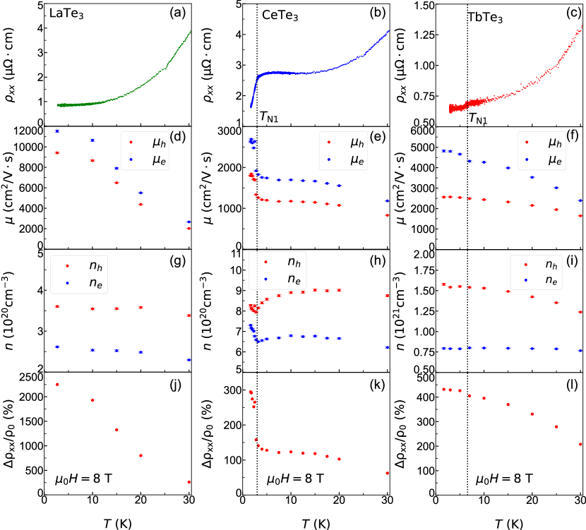
The temperature dependence of the longitudinal resistivity for LaTe3, CeTe3, and TbTe3 devices are shown in Fig. 1(c). All these show metallic temperature dependencies even below the CDW transition. This is due to the partial gap opening, caused by the imperfect nesting of the FS [13]. The residual resistivity ratios (RRRs) (), which are indicators of the purity of the devices, were 98 for LaTe3, 17 for CeTe3, and 45 for TbTe3. These values are larger than previous studies for TbTe3 films [32] and comparable to our previous study for CeTe3 [16]. Although no previous studies have been reported for LaTe3 thin films, the RRR values are comparable to the bulk counterpart [25].
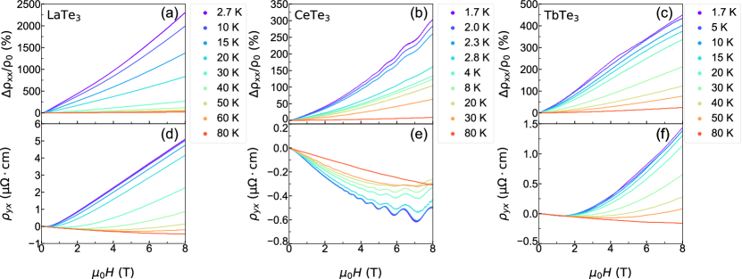
We next performed longitudinal MR and Hall resistance measurements at various temperatures from around 100 K down to 1.7 K. The longitudinal and Hall resistances are symmetrized and antisymmetrized with respect to the magnetic field to extract only their respective components. In Figs. 2(a)-2(c), we show the magnetic field dependence of MR ratio defined as for (a) LaTe3, (b) CeTe3, and (c) TbTe3 devices. For all the devices, a non-saturating and large positive MR were observed. These are characteristics of materials with high carrier mobilities ( is larger than cmVs). Especially for LaTe3, the MR ratio reached up to 2250% at 2.7 K, which is larger than its bulk counterpart by a rough factor of 3 [25]. This is likely due to the increase in the crystallinity of the thin film device, compared to the bulk counterpart, by exfoliation and selection of clean flakes. In contrast to the parabolic field dependence of MR due to the usual Lorentz force contribution in CeTe3, linear MRs were observed for both LaTe3 and TbTe3 at low enough temperatures. These linear MR were also observed in previous studies of bulk LaTe3 and thin-film TbTe3 devices [25, 33, 32, 34]. Furthermore, in the AFM phase of TbTe3 below the Néel temperature ( K), the slope of MR is changed at T [see K in Fig. 2(c)]. This magnetic field of the change of the MR slope is close to the phase transition magnetic field reported in the previous study [31]. It seems that the AFM structure has a notable effect on the electrical transport properties.
The Hall resistance, which was taken simultaneously with the MR, is shown as the Hall resistivity in Figs. 2(d)-2(f) for (d) LaTe3, (e) CeTe3, and (f) TbTe3 devices. All the curves show nonlinear external field dependencies. This behavior was reproducible for all of , , and devices, suggesting that these materials possess multiple carriers. From the Hall curves, we derived the carrier mobilities and concentrations, which will be detailed in the next subsection. It should be noted that quantum oscillations were observed in the case of CeTe3 both in the longitudinal and Hall resistivities. The observation of quantum oscillation in the longitudinal MR is consistent with our previous studies [16, 27], while the emergence of the quantum oscillation in the Hall effect can be attributed to the multi-carrier effect [35]. The analysis of this SdH signal will be discussed in Sec. III C.
III.2 Effect of magnetic order on the electrical transport
In order to investigate the effect of magnetic order on the electrical transport, we have analyzed the temperature dependence of the zero field longitudinal resistivity, carrier mobility, carrier concentration, and MR ratio for each material as shown in Fig. 3. First, we discuss the temperature dependence of the longitudinal resistivity in the low temperature region. In and which are known to have a multi-AFM phase, reductions in the zero field resistivity were observed below the first magnetic transition temperature K and K, respectively [11, 31]. Enlarged views of the low-temperature region of the electrical resistivities of CeTe3 and TbTe3 with magnetic transition points are shown in Figs. 3(b) and 3(c), respectively. The electrical resistivity of nonmagnetic LaTe3 is shown in Fig. 3(a) for comparison, where no characteristic reduction was observed. These reductions in for CeTe3 and TbTe3 can be attributed to the suppression of magnetic scattering by magnetic ordering. It is clear that this effect is especially pronounced in CeTe3 compared to TbTe3. This result indicates that the Ruderman–Kittel–Kasuya–Yosida (RKKY) interaction plays an important role in the magnetism and transport properties in CeTe3. In fact, the electrical resistivity of CeTe3 also has a small bump at around 5 K as shown in Fig. 3(b) [16]. This is likely due to a weak Kondo effect [9], which is further supportive evidence of the AFM coupling in the conduction electron of CeTe3.
Next we discuss the temperature dependence of the carrier mobility and concentration calculated from the MR and the Hall resistivity. Assuming the presence of independent electron and hole carriers, we have considered the conventional two-band model for analysis and used the following equations,
| (1) | ||||
| (2) |
where and are the longitudinal and Hall conductivities, respectively, is the elementary charge, is the applied magnetic field, and are the carrier concentrations of hole and electron, and and are the carrier mobilities of hole and electron, respectively. Here we have assumed and used the Onsager’s reciprocal relation to derive the electrical conductivity from the electrical resistivity. Carrier mobilities and concentrations have been determined by fitting the measured data by the two-band model in Eqs. (1) and (2) simultaneously.
Although the equations have been well-fitted in most temperatures, some discrepancy from the data have been observed at the lower temperatures, as shown in Fig. S1 (in Supplemental Materials). This could be due to the following three main reasons. The first reason is the linear MR; while the linear MR was clearly observed, the MR described by the usual two-band model is parabolic on magnetic field, leading to a difference in fitting. The second possibility would be anisotropy in the electrical resistivity; the assumption was used in the conversion from electrical resistivity to conductivity, but it is known that the Te3 system exhibits significant anisotropy of electrical resistivity with respect to the crystal axis below the CDW transition temperature. In fact, enhancement of the anisotropy at lower temperatures has been reported in some Te3 materials, [36, 31], which could be the cause of errors in the fitting. The third possibility would be multi-carriers; although two-band carriers are considered here for simplicity, it is likely that more types of carriers contribute to transport in reality, and the equation for the two-band model may not reflect the actual situation. In fact, in the Te3 system, the existence of more than two carriers has been suggested from measurements of SdH quantum oscillations [8, 17]. In addition, it is possible that the transport properties unique to the magnetic structure, such as the anomalous Hall effect, may also contribute to the discrepancy.
The results of carrier mobilities and concentrations for electron and hole obtained by the two-band model are shown in Figs. 3(d)-3(f), and Figs. 3(g)-3(i) for LaTe3, CeTe3, and TbTe3 devices, respectively. The electron mobility of is cm2/Vs at 2.7 K, which is notably high, and the order of magnitude is comparable to that of GdTe3 [8], NdTe3 [17] and bulk LaTe3 [25], which were reported as high mobility Te3 systems. The high mobility common to the Te3 system originates from the small pocket created by the reconstruction of the FS due to the CDW ordering [37]. In terms of the effect of the magnetic ordering, enhancements of carrier mobilities below are observed for AFM TbTe3 and CeTe3. As for CeTe3, the carrier mobilities reach up to a total enhancement of 44%. The only other Te3 material reported to have such a large mobility enhancement below its magnetic transition temperature is [17]. Similar to the temperature dependence of longitudinal resistivity, the origin of this behavior would be the enhancement of electron relaxation time due to the suppression of magnetic scattering by magnetic ordering.
The effect of magnetic ordering is also observed in the temperature dependence of the MR ratio. In Figs. 3(j)-3(l), we have plotted the temperature dependence of the MR ratio at 8 T for (j) LaTe3, (k) CeTe3, and (l) TbTe3 devices. While a gradual increase in the MR ratio with decreasing temperature is observed for the nonmagnetic LaTe3, discontinuous enhancements of the MR ratio below the first magnetic transition temperature are observed for CeTe3 and TbTe3. In particular, a sharp increase of 111% is observed for CeTe3 below . These enhancements of the MR ratio can be explained by the increase in the carrier mobility below . On the other hand, we did not observe any negative MR which is often observed in typical magnetic materials. This is likely attributed to the fact that the positive MR effect caused by high carrier mobility overwhelms the negative MR component.
Let us mention the change in the temperature dependence of carrier concentration below and above observed for CeTe3, as shown in Fig. 3 (h). Although the transport phenomena discussed in this section can be attributed to the scattering by the fluctuating magnetic moments, the change in and cannot be explained by the same mechanism. Usually, magnetic transition is not accompanied by a drastic change in its carrier concentration. Rather, we believe that modulation of the CDW, which is closely related to the band structure of the material, could be the direct cause of the carrier concentration temperature dependence. Given that this behavior occurs at , the data implies that there is some coupling of the CDW and magnetic order. As far as we know, neutron diffraction experiments have been conducted for TbTe3 [18, 19], where in addition to the commensurate AFM and CDW orders, new magnetic peaks were observed whose propagation vector equals the sum of the AFM and CDW propagation vectors, revealing a coupling between the orders. Although there is no evidence for CeTe3, the magnetic ordering in CeTe3 may modulate the CDW state, resulting in a change of the temperature dependence in and . It is also interesting to note that this effect is pronounced in CeTe3, indicating that the RKKY interaction, which is more significant in CeTe3, is a possible origin of the coupling between the CDW and the magnetic order.
III.3 Shubnikov-de Haas oscillations
SdH oscillations have been reported in several Te3 materials [8, 17, 38, 39], where the structure of the FS plays an important role [13, 37]. In this subsection, we discuss the effect of magnetic order on the SdH oscillations. As mentioned in Sec. III A., in CeTe3, SdH oscillations were observed in the MR, i.e., [see Fig. 2(b)]. In addition, quantum oscillations with the same period as the SdH oscillations were also observed in the Hall resistivity component, i.e., [see Fig. 2(e)]. In general, SdH oscillations are discussed for . It is known that the SdH oscillations are also reflected in for multi-carrier materials [35]. The amplitude of the oscillations in becomes larger than that in . Thus, we have used the oscillatory component of for the following analysis of the quantum oscillations, but as shown in Fig. S3 (in Supplemental Materials), we have obtained the essentially same result in .
In general, the SdH oscillation is described by the following Lifshitz-Kosevich (L-K) formula with as the oscillating component of resistance, given as
| (3) |
where is the Dingle temperature which corresponds to the blurring of the Landau level, and is the frequency of the SdH oscillation. is the Berry phase and is the phase shift that takes zero in 2D and in 3D systems. is defined by , where is the Boltzmann constant, is the reduced Planck constant, and is the effective cyclotron mass.
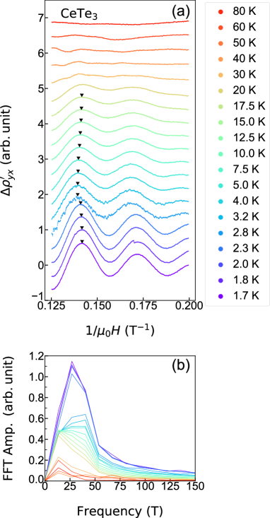
First, we analyze the SdH frequency in order to determine the FS structure responsible for the oscillation, using the equation where is the extremal surface area of the FS pocket. For the analysis, the background resistivity was first subtracted from the Hall resistivity in the magnetic field range from 5 T to 8 T and the the oscillatory component was obtained as shown in Fig. 4(a). We then performed the fast Fourier transformation (FFT) to extract the oscillation frequency. A single oscillation frequency of T was observed as shown in Fig. 4(b), which is consistent with our previous study [16]. Given that the 3D unit cell of Te3 is equal to the unit cell of a single Te square-net rotated by 45 degrees and multiplied by 2 [40], the size of the Brillouin zone of CeTe3 can be calculated as , where Å, Å [41]. Therefore, we determine that the measured SdH oscillation originates from a FS pocket equivalent to 0.30% of the entire Brillouin zone, which is likely the small FS pocket frequently labeled as the pocket in Te3. This pocket arises due to the reconstruction of the FS under the CDW ordering, and was also observed in other Te3 (0.28% for LaTe3 [39], 0.27% for GdTe3 [8], 0.2% for NdTe3 [17], and 0.160.1% for NdTe3 measured by angle-resolved photoemission spectroscopy (ARPES) [37]).
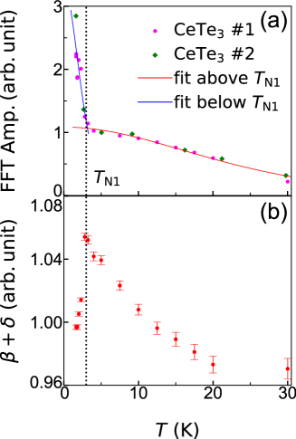
Next, we discuss the temperature dependence of the SdH oscillation amplitude, from which the conduction electron effective mass and mobility can be evaluated. The SdH oscillation amplitude has a characteristic temperature dependence that is proportional to , where is the mean value of the analyzed magnetic field range. By fitting the FFT amplitude with the above function as shown in Fig. 5(a), the effective mass can be obtained. We note that data from multiple samples are plotted in Fig. 5(a), which are normalized by the FFT amplitude at 5 K. The results are listed in Table 1. Above , the effective mass is 0.042, which is comparable to our previous work [16]. A large deviation from the L-K formula has been observed below . Thus, we performed separate fits for the effective mass above and below , resulting in a large enhancement of effective mass (0.37) below . The quantum life time and the carrier mobility can also be evaluated as listed in Table 1. We have observed an enhancement in all , and below . It is important to note that these enhancements provide further supportive evidence of our discussion based on the MR and Hall resistivity in Sec. III B. The enhancement of below is most likely attributed to some modulation of the band structure near the FS from the magnetic order, which is consistent with our analysis of the temperature dependence of the carrier concentrations. The enhancement of carrier mobility is also consistent with the temperature dependence of longitudinal and Hall resistivities. It should originate from the increase in relaxation time of the carriers as the fluctuations of magnetic moments are suppressed below .
Finally, we point out the term in Eq. (3). As mentioned, the and terms correspond to the Berry curvature and the dimension of the FS pocket, respectively. The temperature dependence of is shown in Fig. 5(b), where a peak structure is observed at . This phase shift can also be seen in the shift of the position of the oscillation peaks shown in Fig. 4(a). Although further study is required to elucidate the origin of this behavior, it is another supportive data which indicates the modulation of the band structure near the FS around , since this quantity should be sensitive to the FS topology.
| region | ||||
|---|---|---|---|---|
| PM (10 K) | 0.042 | 48.3 | 1056 | |
| AFM (1.7 K) | 0.37 | 2.53 | 2266 |
IV Conclusion
In this work, we have focused on Te3, a van-der-Waals material with high mobility. We performed systematic longitudinal resistivity and Hall resistivity measurements on single-crystal thin films of nonmagnetic LaTe3 and antiferromagnetic CeTe3 and TbTe3. We have observed a peculiar linear magnetoresistance in LaTe3 and TbTe3, the magnetic field dependence of nonlinear Hall resistance in all samples, and a SdH oscillation in CeTe3. Carrier concentration and mobility are derived using a two band model. Both CeTe3 and TbTe3 show decreases in longitudinal resistivity and increases in carrier mobility below . Combined with the quantum mobility obtained from the SdH oscillation in CeTe3, we conclude that the behavior is caused by the suppression of magnetic scattering due to the magnetic ordering. Furthermore, a change in the temperature dependence of the carrier concentration is also observed in CeTe3 below and above its magnetic transition temperature. Combined with the results of L-K formula fitting, we have found that the band structure near the FS may be modulated by the magnetic ordering. This indicates that the magnetic ordering and CDW ordering are coupled via the RKKY interaction. It is expected that further ARPES experiments before and after the magnetic transition will be performed to search for interesting properties in the system where CDW and magnetic order are strongly coupled. Our results demonstrates not only possibilities of two-dimensional devices with high mobility and magnetic order, but also a test-bed towards the understanding of new phenomena due to the coexistence of magnetic order and CDW order in low-dimensional materials.
V Data Availability
The data that support the findings of this study are available from the corresponding author upon reasonable request.
VI Acknowledgements
We thank S. Nakaharai for his technical supports and fruitful discussions. This work was supported by JSPS KAKENHI (Grant Nos. JP20H02557, JP21J20477, JP22H04481, JP23H00257, and JP23K13062) and JST FOREST (Grant No. JPMJFR2134).
References
- [1] J. F. Sierra, J. Fabian, R. K. Kawakami, S. Roche, and S. O. Valenzuela, Nat. Nanotechnol. 16, 856-868 (2021).
- [2] C. Tan, J. Lee, S. Jung, T. Park, S. Albarakati, J. Partridge, M. R. Field, D. G. McCulloch, L. Wang, and C. Lee, Nat Commun 9, 1554 (2018).
- [3] W. Xing, L. Qiu, X. Wang, Y. Yao, Y. Ma, R. Cai, S. Jia, X. C. Xie, and W. Han, Phys. Rev. X 9, 011026 (2019).
- [4] D. R. Klein, D. MacNeill, J. L. Lado, D. Soriano, E. Navarro-Moratalla, K. Watanabe, T. Taniguchi, S. Manni, P. Canfield, J. Fernández-Rossier, P. Jarillo-Herrero, Science 360, 1218-1222 (2018).
- [5] S. Jiang, J. Shan, and K. F. Mak, Nature Mater 17, 406-410 (2018).
- [6] Z. Wang, T. Zhang, M. Ding, B. Dong, Y. Li, M. Chen, X. Li, J. Huang, H. Wang, X. Zhao, Y. Li, D. Li, C. Jia, L. Sun, H. Guo, Y. Ye, D. Sun, Y. Chen, T. Yang, J. Zhang, S. Ono, Z. Han, and Z. Zhang, Nature Nanotech 13, 554-559 (2018).
- [7] X. Cui, G. Lee, Y. D. Kim, G. Arefe, P. Y. Huang, C. Lee, D. A. Chenet, X. Zhang, L. Wang, F. Ye, F. Pizzocchero, B. S. Jessen, K. Watanabe, T. Taniguchi, D. A. Muller, T. Low, P. Kim, and J. Hone, Nature Nanotech 10, 534-540 (2015).
- [8] S. Lei, J. Lin, Y. Jia, M. Gray, A. Topp, G. Farahi, S. Klemenz, T. Gao, F. Rodolakis, J. L. McChesney, C. R. Ast, A.Yazdani, K. S. Burch, S. Wu, N. Phuan Ong, and L. M. Schoop, Sci. Adv. 6, eaay6407 (2020).
- [9] N. Ru and I. R. Fisher, Phys. Rev. B 73, 033101 (2006).
- [10] E. DiMasi, B. Foran, M. C. Aronson, and S. Lee, Chem. Mater. 6, 1867 (1994).
- [11] Y. Iyeiri, T. Okumura, C. Michioka, and K. Suzuki, Phys. Rev. B 67, 144417 (2003).
- [12] E. DiMasi, M. C. Aronson, J. F. Mansfield, B. Foran, and S. Lee, Phys. Rev. B 52, 14516 (1995).
- [13] V. Brouet, W. L. Yang, X. J. Zhou, Z. Hussain, R. G. Moore, R. He, D. H. Lu, Z. X. Shen, J. Laverock, S. B. Dugdale, N. Ru, and I. R. Fisher, Phys. Rev. B 77, 235104 (2008).
- [14] J. Laverock, S. B. Dugdale, Zs. Major, M. A. Alam, N. Ru, I. R. Fisher, G. Santi, and E. Bruno, Phys. Rev. B 71, 085114 (2005).
- [15] N. Ru, C. L. Condron, G. Y. Margulis, K. Y. Shin, J. Laverock, S. B. Dugdale, M. F. Toney, and I. R. Fisher, Phys. Rev. B 77, 035114 (2008).
- [16] M. Watanabe, R. Nakamura, S. Lee, T. Asano, T. Ibe, M. Tokuda, H. Taniguchi, D. Ueta, Y. Okada, K. Kobayashi, and Y. Niimi, AIP Advances 11, 015005 (2021).
- [17] K. J. Dalgaard, S. Lei, S. Wiedmann, M. Bremholm, and L. M. Schoop, Phys. Rev. B 102, 245109 (2020).
- [18] F. Pfuner, S. N. Gvasaliya, O. Zaharko, L. Keller, J. Mesot, V. Pomjakushin, J-H. Chu, I. R. Fisher, and L. Degiorgi, J. Phys.: Condens. Matter 24, 036001 (2012).
- [19] S. Chillal, E. Schierle, E. Weschke, F. Yokaichiya, J.-U. Hoffmann, O. S. Volkova, A. N. Vasiliev, A. A. Sinchenko, P. Lejay, A. Hadj-Azzem, P. Monceau, and B. Lake, Phys. Rev. B 102, 241110(R) (2020).
- [20] A. Raghavan, M. Romanelli, J. May-Mann, A. Aishwarya, L. Aggarwal, A. G. Singh, M. D. Bachmann, L. M. Schoop, E. Fradkin, I. R. Fisher, and V. Madhavan, arXiv:2308.15691 (2023).
- [21] N. Yamamoto, R. Kondo, H. Maeda, and Y. Nogami, J. Phys. Soc. Jpn. 82, 123701 (2013).
- [22] F. Galli, S. Ramakrishnan, T. Taniguchi, G. J. Nieuwenhuys, J. A. Mydosh, S. Geupel, J. Lüdecke, and S. van Smaalen, Phys. Rev. Lett. 85, 158 (2000).
- [23] X. Teng, L. Chen, F. Ye, E. Rosenberg, Z. Liu, J. Yin, Y. Jiang, J. S. Oh, M. Z. Hasan, K. J. Neubauer, B. Gao, Y. Xie, M. Hashimoto, D. Lu, C. Jozwiak, A. Bostwick, E. Rotenberg, R. J. Birgeneau, J. Chu, M. Yi, and P. Dai, Nature 609, 490-495 (2022).
- [24] T. Shang, Y. Xu, D. J. Gawryluk, J. Z. Ma, T. Shiroka, M. Shi, and E. Pomjakushina, Phys. Rev. B 103, L020405 (2021).
- [25] A. Pariari, S. Koley, S. Roy, R. Singha, M. S. Laad, A. Taraphder, and P. Mandal, Phys. Rev. B 104, 155147 (2021).
- [26] W. S. Lee, A. P. Sorini, M. Yi, Y. D. Chuang, B. Moritz, W. L. Yang, J.-H. Chu, H. H. Kuo, A. G. Cruz Gonzalez, I. R. Fisher, Z. Hussain, T. P. Devereaux, and Z. X. Shen, Phys. Rev. B 85, 155142 (2012).
- [27] M. Watanabe, S. Lee, T. Asano, T. Ibe, M. Tokuda, H. Taniguchi, D. Ueta, Y. Okada, K. Kobayashi, and Y. Niimi, Appl. Phys. Lett. 117, 072403 (2020).
- [28] R. Okuma, D. Ueta, S. Kuniyoshi, Y. Fujisawa, B. Smith, C. H. Hsu, Y. Inagaki, W. Si, T. Kawae, H. Lin, F. C. Chuang, T. Masuda, R. Kobayashi, and Y. Okada, Sci Rep 10, 15311 (2020).
- [29] D. Ueta, R. Kobayashi, H. Sawada, Y. Iwata, S. Yano, S. Kuniyoshi, Y. Fujisawa, T. Masuda, Y. Okada, and S. Itoh, J. Phys. Soc. Jpn. 91, 094706 (2022).
- [30] J. Kopaczek, K. Yumigeta, A. Ibrahim, M. Y. Sayyad, S. Sinha, R. Sailus, P. Hays, S. Tohid Rajaei Moosavy, S. Susarla, C. Ataca, R. Kudrawiec, and S. Tongay, Adv. Electron.Mater. 9, 2201129 (2023).
- [31] O. S. Volkova, A. Hadj-Azzem, G. Remenyi, J. Emilio Lorenzo, P. Monceau, A. A. Sinchenko, and A. N. Vasiliev, Materials 15(24), 8772 (2022).
- [32] Y. Xing, Y. Li, Z. Yang, Z. Wang, P. Yang, J. Ge, Y. Liu, Y. Liu, T. Luo, Y. Tang, and J. Wang, J. Appl. Phys. 128, 073901 (2020).
- [33] A. A. Sinchenko, P. D. Grigoriev, P. Lejay, and P. Monceau, Phys. Rev. B 96, 245129 (2017).
- [34] A. V. Frolov, A. P. Orlov , P. D. Grigoriev, V. N. Zverev, A. A. Sinchenko, and P. Monceau, Jetp Lett. 107, 488-492 (2018).
- [35] N. Kikugawa, A. W. Rost, C. W. Hicks, A. J. Schofield, and A. P. Mackenzie, J. Phys. Soc. Jpn. 79, 024704 (2010).
- [36] A. A. Sinchenko, P. D. Grigoriev, P. Lejay, and P. Monceau, Phys. Rev. Lett. 112, 036601 (2014).
- [37] A. Chikina, H. Lund, M. Bianchi, D. Curcio, K. J. Dalgaard, M. Bremholm, S. Lei, R. Singha, L. M. Schoop, and P. Hofmann, Phys. Rev. B 107, L161103 (2023).
- [38] P. Walmsley, S. Aeschlimann, J. A. W. Straquadine, P. Giraldo-Gallo, S. C. Riggs, M. K. Chan, R. D. McDonald, and I. R. Fisher, Phys. Rev. B 102, 045150 (2020).
- [39] N. Ru, R. A. Borzi, A. Rost, A. P. Mackenzie, J. Laverock, S. B. Dugdale, and I. R. Fisher, Phys. Rev. B 78, 045123 (2008).
- [40] V. Brouet, W. L. Yang, X. J. Zhou, Z. Hussain, N. Ru, K. Y. Shin, I. R. Fisher, and Z. X. Shen, Phys. Rev. Lett. 93, 126405 (2004).
- [41] T. T. Han, Z. Tao, S. D. Mahanti, K. Chang, C. Ruan, C. D. Malliakas, and M. G. Kanatzidis, Phys. Rev. B 86, 075145 (2012).