Impacts of Point Defects on Shallow Doping in Cubic Boron Arsenide: A First Principles Study
Abstract
Cubic boron arsenide (BAs) stands out as a promising material for advanced electronics, thanks to its exceptional thermal conductivity and ambipolar mobility. However, effective control of p- and n-type doping in BAs poses a significant challenge, mostly as a result of the influence of defects. In the present study, we employed density functional theory to explore the impacts of the common point defects and impurity on p-type doping Be and Si, and n-type doping Si and Se. We find that the most favorable points defects formed by C, O, and Si are C, OO, Si, CSi, and OSi, which have formation energies of less than eV. For p-type doping, C, O, and Si impurities do not harm the shallow state of Be doping, while only O impurity detrimentally affects Si doping. However for n-type dopings, C, O, and Si impurities are all harmful. Interestingly, the antisite defect pair AsB benefits both p- and n-type doping. The doping limitation analysis presented in this study can potentially pave the way for strategic development in the area of BAs-based electronics.
Over the last decade, cubic boron arsenide (BAs) has attracted an extremely high level of research interest, due to its exceptional thermal conductivity and ambipolar mobility. The thermal conductivity of BAs (i.e., 1300 W/mK at room temperature, which is only surpassed by diamond for bulk materials) was first predicted via theory [1, 2, 3], then validated by experiments [4, 5, 6]. The simultaneously high room-temperature electron and hole mobilities were also predicted by theory [7] and later confirmed through recent experiments [8, 9]. Beyond its remarkable transport properties, BAs is applicable to existing III–V semiconductor technology [10], and has an electronic structure similar to that of Si, but with a wider band gap [11]. These attributes position BAs as a promising material for advanced electronics and efficient heat management.
One critical need in high-performance electronic applications relates to the development of methodologies to control p- and n-type doping, in order to generate the desired ionizable delocalized (shallow) impurity states [12]. To accomplish this, the behaviors of defects such as intrinsic defects and impurities must be comprehensively understood. Despite the successful synthesis of millimeter-sized BAs crystals, achieved via the chemical vapor transport method [13, 14, 15, 16], a substantial variance is still observed in the measured thermal properties of BAs [5, 17, 18, 19]. Coupled with the observation of p-type semiconducting behavior [15, 19, 20], these results indicate the presence of intrinsic defects and impurities in BAs samples. While extensive research [21, 22, 23, 24, 8, 25] has been performed on the thermal conductivity reduction caused by intrinsic defects and impurities, comparably less emphasis has been placed on comprehending how intrinsic defects and impurities affect electronic properties. Notably, first principles calculations [21, 26, 27] were utilized to explore the formation of intrinsic defects, identifying the antisite pair AsB as being the most prevalent intrinsic defect type. However, the antisite pair AsB is usually neutral and thus cannot explain the observed p-type semiconducting behavior. Theoretical studies attribute the p-type semiconducting behavior of BAs to impurities, such as Si, C, and H [26, 27], whereas recent experiments have validated the presence of Si, C, O, H, Te, and I impurities in BAs [24].
Furthermore, the first principles calculations identified specific dopants (e.g., Be and Si for p-type, and Si and Se for n-type) characterized as shallow dopants [26, 27]. A high p-dopability of BAs is also reported [27, 28]. However, the behaviors of shallow dopants can be influenced by point defects, as the aforementioned impurities can solely induce p-type behavior. Notably, how various point defects influence the behaviors of shallow dopants have never comprehensively been investigated. Thus, for the present work, we conduct a detailed thermodynamic analysis demonstrating the interaction between point defects and shallow dopants utilizing density functional theory (DFT).
In the present work, the DFT calculations were carried out using the projector augmented-wave method [29, 30], as implemented in the Vienna ab initio Simulation Package code [31, 32]. The employed exchange correlation functional was the generalized gradient approximation (GGA) as formulated by Perdew, Burke, and Ernzerhof functional revised for solids (PBEsol) [33]. Notably, previous DFT calculations [26, 27] utilized the Heyd-Scuseria-Ernzerhof (HSE) functional[34], which, as compared to the PBE functional, can more accurately predict the band gap but has a considerably higher computational cost, limiting its use in exploring different configurations involving both dopants and point defects. In Sec. II of the Supplemental Materials (SM) [35], we compute the formation energy of p- and n-type dopants using PBEsol, and comparable results were obtained between PBEsol and HSE results from Ref. [26, 27]. We therefore use PBEsol throughout this work. For all calculations, spin polarization, a plane-wave cutoff energy of 700 eV, and an energy convergence criterion of eV were applied. For the defect calculations, a supercell of the conventional cubic cell (216 atoms) and a -centered k-point mesh were employed, as used by previous study [12]. The total charge of the defected systems was kept neutral. The relaxed lattice parameter of the conventional cubic cell of BAs was 4.778 Å.
The key properties computed are the formation energies and the isosurfaces of charge density. The formation energy values quantified the ease of defect formation, while the isosurfaces of charge density were employed to visualize the spatial localization of impurity states. The formation energy of a given defect (or dopant) is calculated as:
| (1) |
where is the total energy of the pristine system, is the total energy of the defected system, is the change in the number of atoms of species due to defect (positive if atoms are added, negative if atoms are removed), is the energy per atom in the elemental phase, and is the chemical potential of species . The elemental phases of species B, As, C, O, Si, Be, and Se were considered using -B, -As, graphene, oxygen gas, Si in the diamond structure, Be in the hexagonal close-packed structure, and -Se, respectively. For all species , . Furthermore, for all impurity atoms and dopants, was approximated as zero. The values of and depend on the growth condition involved: in the As-rich condition, ; otherwise, in the B-rich condition. Additionally, and are restricted by the equilibrium condition , where is the formation enthalpy of BAs. Throughout this work, we use the As-rich condition, following Ref. [21]. Nevertheless, the PBEsol-predicted value of is merely eV, meaning that the differences in (or ) between As- and B-rich conditions only total eV, which is trivial. Assuming a defect is already present in the system, the formation energy of a dopant can be determined using the formula , where is the formation energy when both the dopant and the defect coexist (see Sec. I of SM [35] for more details). Comparing against affords insight into whether the defect is advantageous for the formation of the dopant . The isosurfaces of charge density were visualized using the VESTA package [36]. Additionally, X was used to represent a substitutional X atom in the Y site.
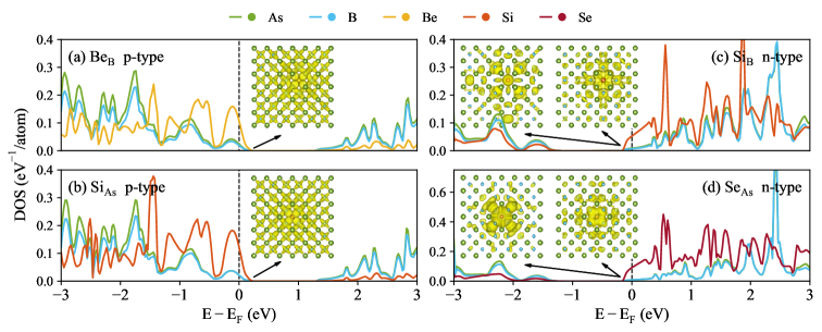
Here we begin by identifying the dopants. HSE calculations [26, 27] suggest p-type dopants Be and Si and n-type dopants Se and Si are shallow dopants with low formation energy. Using PBEsol (see Sec. II of SM [35] for more details), our results also confirm that the formation energies of Be ( eV), Si ( eV), Si ( eV), and Se ( eV) are the lowest among the computed dopants. Note that for p-type doping (Be and Si), the formation energy is substantially lower than that for n-type doping (Se and Si), thus supporting the notion that p-type doping occurs more readily in BAs than n-type [26, 27]. In addition, the electronic density of states (DOS) and isosurface of charge density were computed for Be, Si, Si, and Se (see Fig. 1). For Be and Si, while the Fermi level slightly shifts into the valence bands, there are three-fold degenerated bands at VBM, and their isosurfaces of charge density exhibit strong spatially delocalized natures, directly revealing Be and Si to be shallow acceptor impurities. For Se and Si, slightly shifts into the conduction bands. Two bands with moderate delocalization are observed: one with its bottom at CBM (inset figures on the left) and the other with its bottom within 0.1 eV of CBM (inset figures on the right), showing that both Se and Si are shallow donor impurities. Therefore, Be, Si, Si, and Se were selected for further investigation regarding the influence of point defects, in terms of four different cases: p- and n-type dopants on both B and As sites.
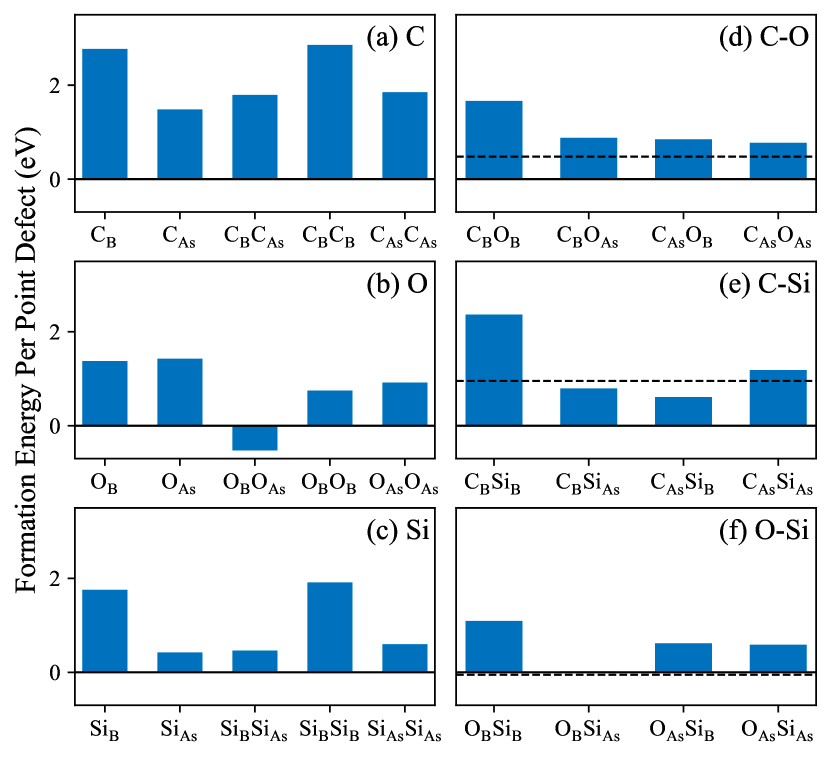
Given the multitude of configurations involving different species and atom sites for point defects, it is imperative to select the most representative ones. First, we considered C, O, and Si as the impurity elements, due to their high concentration as substitutional impurities, as reported in Ref. [24]. Secondly, we restricted our consideration to single point defects and point defect pairs in the first nearest neighbor. For each situation, only the point defect with the lowest formation energy was investigated further. Fig. 2 presents the calculation results. Panels (a), (b), and (c) reflect situations in which individual C, O, and Si impurities existed, respectively, whereas panels (d), (e), and (f) reflect situations in which combinations of C and O, C and Si, and O and Si impurities coexisted, respectively. Please note that, for a direct comparison, the y-axis value is the formation energy per point defect, meaning that the formation energy of defect pairs is divided by two. From Fig. 2(a)–(c), C, OO, and Si are the most favorable point defects when C, O, and Si are the only impurity elements, respectively. In Fig. 2(d), rather than forming defect pairs, C and O impurities are more likely to form isolated C and OO (indicated by the dashed line). In contrast, C and Si atoms are more likely to form CSi, as opposed to isolated C and Si (indicated by the dashed line). When O and Si coexist, the formation energy per point defect of OSi is eV, and the mean formation energy per point defect of OO and Si is eV (see Fig. 2(f)). Given the small difference (0.14 eV) between these two values, we exceptionally count in OSi into further investigation. To summarize, we selected C, OO, Si, CSi, and OSi as representative point defects of impurity.
![[Uncaptioned image]](/html/2403.09013/assets/x4.png)
![[Uncaptioned image]](/html/2403.09013/assets/x5.png)
![[Uncaptioned image]](/html/2403.09013/assets/x6.png)
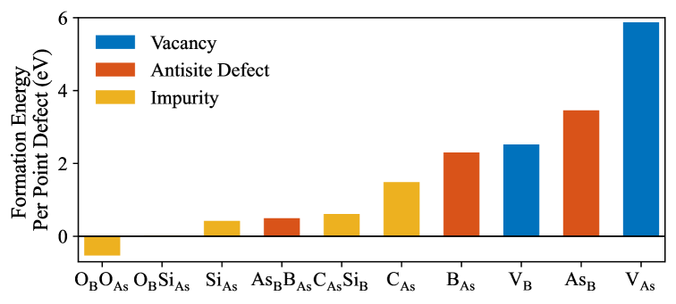
We also examine the intrinsic point defects, including antisite single defects As and B, antisite defect pair AsB, and single vacancies V and V. The formation energy per point defect for each of these intrinsic defects is plotted alongside the selected point defects of impurities, moving from the smallest formation energy (left) to the largest (right) (see Fig. 3). Certainly, only the antisite defect pair AsB has a formation energy comparable to that of the selected point defects of impurity. Thus, we will discuss a total of six types of point defects, including the aforementioned five selected types of impurities plus AsB, where the formation energies per point defect are all less than eV.
Finally, we discuss the impact of these common point defects (AsB, C, OO, Si, C, Si, and OSi) on both the formation energy and the electronic characteristics of shallow dopants Be, Si, Si, and Se. Please note that, with respect to Si being regarded as a p-type dopant, Si itself is no longer categorized as a point defect of impurity, while CSi and OSi continue to be considered as impurities due to the presence of C and O. In Sec. IV of SM [35], we consider additional point defects As, B, and N, despite their potential lack of favorability within the BAs system. When different point defects are present, the dopants may occupy various atom sites. For each combination of point defect and dopant, all possible dopant sites within 6Å of the point defects are computed. Sec. III of SM tabulates the detailed calculation results [35]. Here we only focus on the configuration with the lowest total energy and, consequently, the lowest formation energy.
We start with examining the electronic characteristics via the depiction of DOS and isosurfaces of charge density of Be doping (see Fig. 4(a)). As mentioned above, Be and Si feature three-fold degenerated bands at VBM, and the presence of point defects may break the symmetry of the degenerated bands. In this case, only the highest band at VBM is shown as inset figures in Fig. 4(a) and (b), while all bands within 0.1 eV of VBM are provided in enlarged figures in Sec. V of SM [35]. Interestingly, the p-type shallow state of Be is maintained in the presence of all six point defects. is still positioned slightly below VBM, and the bands near VBM continue to exhibit spatial delocalization. This result is understandable for the charge-neutral defects AsB and CSi, as well as for the acceptor-like defects C and Si, though the acceptor-like defects slightly shift the deeper into the valence band. Surprisingly, for the donor-like defects OO and OSi, a delocalized defect state emerges at the top of VBM, while a localized defect state is formed at the bottom of CBM (for OO) or within the band gap (for OSi). Despite the narrowed band gaps, the p-type shallow state of Be is still maintained for both donor-like defects. For the other p-type dopant Si, the results are similar to those for Be; namely, AsB, C, CSi, and OSi all sustain the shallow state (see Fig. 4(b)). The only difference is that OO now forms a localized trapping state in the middle of the band gap, where is positioned.
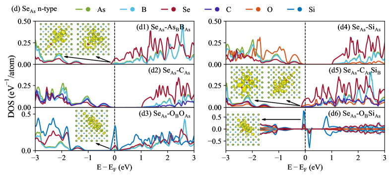
Nevertheless, in the case of n-type dopants Si and Se, the examined point defects exert a more significant influence, owing to the acceptor-like nature of C and Si impurities—for which the is no longer in the conduction bands—thereby destroying the n-type nature (see Fig. 4(c) and (d))). Here, both OO and OSi form localized trapping states within the band gap where is located. As a result, the defects that preserve the n-type shallow state are the charge-neutral defects AsB and CSi, where is marginally above CBM, and one of the bands near CBM exhibits weak spatial delocalization while the other becomes predominantly localized.
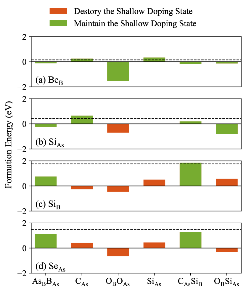
Furthermore, we provide a synopsis regarding the formation energy of dopants in the presence of point defects. The bars in Fig 5 illustrate , the formation energy of the dopants in the presence of each point defect . The dashed black lines denote , the formation energy of the dopants without point defects. Green signifies that the delocalized doping state of the original type is preserved, whereas red indicates otherwise, either because the doping type is changed or the bands near are localized trapping states. This color is defined by the results given in Fig. 4. Three distinct scenarios are covered: (1) a bar above the dashed line implies that the defect does not couple with the dopant, thus merely impacting the doping; (2) a red bar below the dashed line signifies that a coupled complex of the defect and dopant will likely form, potentially compromising the originally targeted doping state; (3) a green bar below the dashed line indicates that the coupled complex will likely form and preserve the shallow doping state. Only the last case is beneficial to the doping efficiency. Following these three scenarios, the O impurity proves detrimental for three types of dopants except Be, as evidenced by the results of OO. This necessitates restriction of O’s concentration. Regarding C and Si, for p-type dopings Be and Si, concerns over C and Si impurities are alleviated; otherwise, for n-type dopings Si and Se, careful removal of C and Si impurities is imperative, which again emphasizes the lower n-type dopability in BAs. Most interestingly, the most favorable intrinsic defect, antisite defect pair AsB, proves beneficial for all four types of dopants. Similar results can be confirmed for the other charge-neutral defect, CSi, which also proves beneficial for three types of dopants except Si.
In conclusion, we have computed the formation energies and electronic characteristics of selected dopants, point defects, and coupled complexes between dopants and point defects in BAs from first principles. The shallow doping states of p-type dopants Be and Si, and n-type dopants Si and Se, were directly confirmed by the delocalized charge density isosurface near . The favorable single point defects and point defect pairs for C, O, and Si impurities were identified (C, OO, Si, CSi, and OSi), all with formation energies of less than eV. As for couplings between the selected dopants and defects, this study also identified the most favorable configurations. In terms of the influence of impurities on doping, the O impurity is detrimental to both p- and n-type doping (except Be), and C and Si impurities are detrimental to only n-type doping. Consequently, n-type doping is challenging, as it has a higher formation energy and requires the removal of C, Si, and O impurities. Interestingly, the most favorable intrinsic defect, antisite defect pair AsB, positively impacts both the p- and n-type doping. These insights into the interactions between dopants and defects could potentially help expedite the advancement of advanced electronics based on BAs.
This work is supported through the INL Laboratory Directed Research and Development (LDRD) Program under DOE Idaho Operations Office Contract DE-AC07-05ID14517, LDRD Project ID 23A1070-064FP. This research made use of Idaho National Laboratory’s High Performance Computing systems located at the Collaborative Computing Center and supported by the Office of Nuclear Energy of the U.S. Department of Energy and the Nuclear Science User Facilities under Contract No. DE-AC07-05ID14517.
References
- Broido et al. [2013] D. A. Broido, L. Lindsay, and T. L. Reinecke, Physical Review B 88, 214303 (2013).
- Lindsay et al. [2013] L. Lindsay, D. A. Broido, and T. L. Reinecke, Physical Review Letters 111, 025901 (2013).
- Feng et al. [2017] T. Feng, L. Lindsay, and X. Ruan, Physical Review B 96, 161201 (2017).
- Kang et al. [2018] J. S. Kang, M. Li, H. Wu, H. Nguyen, and Y. Hu, Science 361, 575 (2018).
- Tian et al. [2018a] F. Tian, B. Song, X. Chen, N. K. Ravichandran, Y. Lv, K. Chen, S. Sullivan, J. Kim, Y. Zhou, T.-H. Liu, M. Goni, Z. Ding, J. Sun, G. A. G. Udalamatta Gamage, H. Sun, H. Ziyaee, S. Huyan, L. Deng, J. Zhou, A. J. Schmidt, S. Chen, C.-W. Chu, P. Y. Huang, D. Broido, L. Shi, G. Chen, and Z. Ren, Science 361, 582 (2018a).
- Li et al. [2018] S. Li, Q. Zheng, Y. Lv, X. Liu, X. Wang, P. Y. Huang, D. G. Cahill, and B. Lv, Science 361, 579 (2018).
- Liu et al. [2018] T.-H. Liu, B. Song, L. Meroueh, Z. Ding, Q. Song, J. Zhou, M. Li, and G. Chen, Physical Review B 98, 081203 (2018).
- Shin et al. [2022] J. Shin, G. A. Gamage, Z. Ding, K. Chen, F. Tian, X. Qian, J. Zhou, H. Lee, J. Zhou, L. Shi, T. Nguyen, F. Han, M. Li, D. Broido, A. Schmidt, Z. Ren, and G. Chen, Science 377, 437 (2022).
- Yue et al. [2022] S. Yue, F. Tian, X. Sui, M. Mohebinia, X. Wu, T. Tong, Z. Wang, B. Wu, Q. Zhang, Z. Ren, J. Bao, and X. Liu, Science 377, 433 (2022).
- Hart and Zunger [2000] G. L. W. Hart and A. Zunger, Physical Review B 62, 13522 (2000).
- Wentzcovitch and Cohen [1986] R. M. Wentzcovitch and M. L. Cohen, Journal of Physics C: Solid State Physics 19, 6791 (1986).
- Joshi et al. [2022] T. Joshi, P. Kumar, B. Poudyal, S. P. Russell, P. Manchanda, and P. Dev, Physical Review B 105, 054101 (2022).
- Xing et al. [2018a] J. Xing, E. R. Glaser, B. Song, J. C. Culbertson, J. A. Freitas, Jr., R. A. Duncan, K. A. Nelson, G. Chen, and N. Ni, Applied Physics Letters 112, 241903 (2018a).
- Tian et al. [2018b] F. Tian, B. Song, B. Lv, J. Sun, S. Huyan, Q. Wu, J. Mao, Y. Ni, Z. Ding, S. Huberman, T.-H. Liu, G. Chen, S. Chen, C.-W. Chu, and Z. Ren, Applied Physics Letters 112, 031903 (2018b).
- Gamage et al. [2019a] G. A. Gamage, H. Sun, H. Ziyaee, F. Tian, and Z. Ren, Applied Physics Letters 115, 092103 (2019a).
- Gamage et al. [2019b] G. A. Gamage, K. Chen, G. Chen, F. Tian, and Z. Ren, Materials Today Physics 11, 100160 (2019b).
- Lv et al. [2015] B. Lv, Y. Lan, X. Wang, Q. Zhang, Y. Hu, A. J. Jacobson, D. Broido, G. Chen, Z. Ren, and C.-W. Chu, Applied Physics Letters 106, 074105 (2015).
- Kim et al. [2016] J. Kim, D. A. Evans, D. P. Sellan, O. M. Williams, E. Ou, A. H. Cowley, and L. Shi, Applied Physics Letters 108, 201905 (2016).
- Xing et al. [2018b] J. Xing, X. Chen, Y. Zhou, James. C. Culbertson, J. A. Freitas, Jr., E. R. Glaser, J. Zhou, L. Shi, and N. Ni, Applied Physics Letters 112, 261901 (2018b).
- Chu and Hyslop [2003] T. L. Chu and A. E. Hyslop, Journal of Applied Physics 43, 276 (2003).
- Zheng et al. [2018] Q. Zheng, C. A. Polanco, M.-H. Du, L. R. Lindsay, M. Chi, J. Yan, and B. C. Sales, Physical Review Letters 121, 105901 (2018).
- Protik et al. [2016] N. H. Protik, J. Carrete, N. A. Katcho, N. Mingo, and D. Broido, Physical Review B 94, 045207 (2016).
- Fava et al. [2021] M. Fava, N. H. Protik, C. Li, N. K. Ravichandran, J. Carrete, A. van Roekeghem, G. K. H. Madsen, N. Mingo, and D. Broido, npj Computational Materials 7, 1 (2021).
- Chen et al. [2021] X. Chen, C. Li, Y. Xu, A. Dolocan, G. Seward, A. Van Roekeghem, F. Tian, J. Xing, S. Guo, N. Ni, Z. Ren, J. Zhou, N. Mingo, D. Broido, and L. Shi, Chemistry of Materials 33, 6974 (2021).
- Tang et al. [2023] J. Tang, G. Li, Q. Wang, J. Zheng, L. Cheng, and R. Guo, Physical Review Materials 7, 044601 (2023).
- Chae et al. [2018] S. Chae, K. Mengle, J. T. Heron, and E. Kioupakis, Applied Physics Letters 113, 212101 (2018).
- Lyons et al. [2018] J. L. Lyons, J. B. Varley, E. R. Glaser, J. A. Freitas, Jr., J. C. Culbertson, F. Tian, G. A. Gamage, H. Sun, H. Ziyaee, and Z. Ren, Applied Physics Letters 113, 251902 (2018).
- Bushick et al. [2019] K. Bushick, K. Mengle, N. Sanders, and E. Kioupakis, Applied Physics Letters 114, 022101 (2019).
- Blöchl [1994] P. E. Blöchl, Physical Review B 50, 17953 (1994).
- Kresse and Joubert [1999] G. Kresse and D. Joubert, Physical Review B 59, 1758 (1999).
- Kresse and Hafner [1993] G. Kresse and J. Hafner, Physical Review B 47, 558 (1993).
- Kresse and Furthmüller [1996] G. Kresse and J. Furthmüller, Physical Review B 54, 11169 (1996).
- Perdew et al. [2008] J. P. Perdew, A. Ruzsinszky, G. I. Csonka, O. A. Vydrov, G. E. Scuseria, L. A. Constantin, X. Zhou, and K. Burke, Physical Review Letters 100, 136406 (2008).
- Heyd et al. [2003] J. Heyd, G. E. Scuseria, and M. Ernzerhof, The Journal of Chemical Physics 118, 8207 (2003).
- [35] See Supplemental Materials at [link] for information about formation energy of charged intrinsic defects in cubic BAs, BP, and BN, formation energy of charged dopants in BAs, calculated configurations of coupled dopants and point defects, calculated DOS and formation energy for extra defects besides the ones presented in the main text, and enlarged figures of isosurfaces of charge density. See also Refs. [37, 38].
- Momma and Izumi [2011] K. Momma and F. Izumi, Journal of Applied Crystallography 44, 1272 (2011).
- Freysoldt et al. [2009] C. Freysoldt, J. Neugebauer, and C. G. Van de Walle, Physical Review Letters 102, 016402 (2009).
- Buckeridge and Scanlon [2019] J. Buckeridge and D. O. Scanlon, Physical Review Materials 3, 051601 (2019).