Performance Analysis of Matrix Multiplication for Deep Learning on the Edge
Abstract
The devices designed for the Internet-of-Things encompass a large variety of distinct processor architectures, forming a highly heterogeneous zoo. In order to tackle this, we employ a simulator to estimate the performance of the matrix-matrix multiplication (gemm) kernel on processors designed to operate at the edge. Our simulator adheres to the modern implementations of gemm, advocated by GotoBLAS2, BLIS, OpenBLAS, etc., to carefully account for the amount of data transfers across the memory hierarchy of different algorithmic variants of the kernel. A small collection of experiments provide the necessary data to calibrate the simulator and deliver highly accurate estimations of the execution time for a given processor architecture.
Keywords:
Performance analysis matrix multiplication high performance IoT processors.1 Introduction
Deep learning (DL) technologies are currently being deployed at the edge in order to improve safety and privacy, reduce the latency for the end-user, and/or decrease energy consumption [4, 7, 12]. The IoT (Internet-of-Things) appliances operating in this scenario comprise a myriad of different processor designs, facing limited computational and memory capacities as well as strict restrictions in power supply and, sometimes, time-to-response. As a consequence, the software running on these devices has to be carefully optimized.
The general matrix-matrix multiplication (gemm) is a key kernel for the realization of the convolutional deep neural networks (DNNs) employed in signal processing and computer vision, as well as for the transformers applied to natural language processing tasks [10]. However, developing an efficient realization of gemm is a time-consuming chore, aggravated by the heterogeneity of IoT architecture designs, which requires a good expertise on high performance computing and computer architecture.
In this paper we contribute toward dealing with the development of optimized realizations of gemm for IoT processors leveraging a performance simulator to experiment with different algorithmic alternatives for this kernel, prior to actually implementing and testing them. Our simulator, built upon the GotoBLAS2 ideas [2] and the BLIS framework [11, 5], mimics the algorithm behavior in order to capture the data transfers across the memory hierarchy, and requires only a few experimental data which can be collected via simple calibration experiments. The result delivers highly accurate estimations of the execution time on an GAP8 parallel-ultra-low power processor (PULP).
2 Blocked Algorithms for GEMM
2.1 The baseline algorithm for GEMM
Consider the gemm , where the dimensions of the matrix operands , and are , and , respectively. Many current high performance realizations of this kernel, in open-source as well as commercial linear algebra libraries, adhere to the GotoBLAS ideas [2] to implement it as a collection of five nested loops around a micro-kernel that performs a tiny gemm. In rough detail, the instances of gemm in these libraries apply tiling (blocking) to the matrix operands so that 1) a block of is packed into a buffer that is intended to reside in the L3 cache memory; 2) an block of is packed into a buffer for the L2 cache memory; and 3) a specific block of , say , is expected to reside in the L1 cache memory during the execution of the micro-kernel. Furthermore, 4) the micro-kernel performs all the arithmetic, retrieving the data of from the L2 cache, from the L1 cache, and directly from memory; see Figure 1. These techniques are adopted, for example, in BLIS [11], OpenBLAS [6], AMD BLIS and, presumably, Intel MKL, among others.
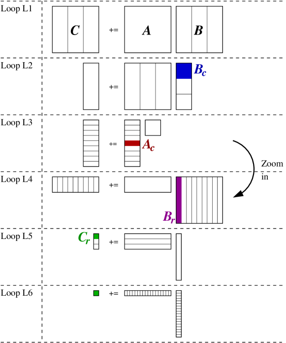 |
               L1 | for ( jc=0; jc<n; jc+=nc )
               L2 |  for ( pc=0; pc<k; pc+=kc ) {
                  |    Bc := B(pc:pc+kc-1,jc:jc+nc-1);   (Mem->L3)
               L3 |    for ( ic=0; ic<m; ic+=mc ) {
                  |      Ac := A(ic:ic+mc-1,pc:pc+kc-1); (Mem->L2)
               L4 |      for ( jr=0; jr<nc; jr+=nr )
               L5 |        for ( ir=0; ir<mc; ir+=mr )
                  |          // Micro-kernel
               L6 |          for ( pr=0; pr<kc; pr++ )
                  |            Cc(ir:ir+mr-1,jr:jr+nr-1) (Mem->Reg)
                  |              +=  Ac(ir:ir+mr-1,pr)   (L2->Reg)
                  |              *   Bc(pr,jr:jrnr-1);   (L1->Reg)
                  |  } }
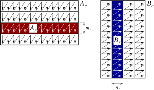 |
The baseline algorithm for gemm presented in this section, hereafter referred to as B3A2C0,111The notation introduced in [9] refers to the baseline algorithm as B3A2C0, where each letter denotes one of the matrix operands, and the subsequent number indicates the cache level where that operand resides (with 0 referring to the processor registers). The same matrix operand resides in both the L1 and L3 caches. features a micro-kernel that comprises a sixth loop, and is usually encoded directly in assembly (or in C with vector intrinsics). At each iteration, this loop updates an micro-tile of , say , by performing an outer product involving (part of) one row of and one column of , as illustrated by loop L6 in Figure 1. The cost of loading/storing can be expected to be amortized over the iterations of this loop, as in practice. Furthermore, a specialized packing of and ensures that their entries are retrieved with unit stride from the micro-kernel; see Figure 2.
2.2 A family of algorithms for GEMM
A different re-ordering of the gemm loops, combined with an appropriate selection of the loop strides, result in other variants for gemm, which favor that the matrix blocks of reside in specific levels of the memory hierarchy, from the main memory to the cache(s) and processor registers. This was analyzed in [9, 3], and more recently, in the context of DL inference, in [1].
Figure 3 shows the algorithms for two of these variants: C3B2A0 and B3C2A0. In the former case, 1) an block of is packed into a buffer for the L3 cache memory; 2) a block of is packed into a buffer for the L2 cache memory; and 3) an block of , say , is intended to reside in the L1 cache memory. In the B3C2A0 case, the roles of and are swapped. Furthermore, 4) in both variants the micro-kernel operates with a micro-tile of , streamed directly from the memory to the registers, performing a small, matrix-vector product per iteration of Loop L6 ( iterations), each involving a single column of and (part of) ; see Figure 3. In addition, in order to ensure accessing the entries of and with unit stride from the micro-kernel, both and are stored following the same pattern shown for in Figure 2, with also re-organized in micro-panels of rows but in micro-panels of rows.
            L1 | for ( jc=0; jc<n; jc+=nc )
            L2 |  for ( ic=0; ic<m; ic+=mc ) {
               |    Cc = C(ic:ic+mc-1,jc:jc+nc-1);         (Mem->L3)
            L3 |    for ( pc=0; pc<k; pc+=kc ) {
               |      Bc := B(pc:pc+kc-1,jc:jc+nc-1);      (Mem->L2)
            L4 |      for ( ir=0; ir<mc; ir+=mr )
            L5 |        for ( pr=0; pr<kc; pr+=kr )
            L6 |          for ( jr=0; jr<nc; jr++ )
               |            Cc(ir:ir+mr-1,jr)              (L1->Reg)
               |              += Ac(ir:ir+mr-1,pc:pc+kr-1) (Mem->Reg)
               |              *  Bc(pc:pc+kr-1,jr);        (L2->Reg)
               |    }
               |    C(ic:ic+mc-1,jc:jc+nc-1) = Cc;         (L3->Mem)
               |  }
               ------------------------------------------------------------
            L1 | for ( jc=0; jc<n; jc+=nc )
            L2 |   for ( pc=0; pc<k; pc+=kc ) {
               |     Bc := B(pc:pc+kc-1,jc:jc+nc-1);        (Mem->L3)
            L3 |     for ( ic=0; ic<m; ic+=mc ) {
               |       Cc := C(ic:ic+mc-1,jc:jc+nc-1);      (Mem->L2)
            L4 |       for ( pr=0; pr<kc; pr+=kr )
            L5 |         for ( ir=0; ir<mc; ir+=mr )
            L6 |           for ( jr=0; jr<nc; jr++ )
               |             Cc(ir:ir+mr-1,jr)              (L2->Reg)
               |               += Ac(ir:ir+mr-1,pc:pc+kr-1) (Mem->Reg)
               |               *  Bc(pc:pc+kr-1,jr);        (L1->Reg)
               |       C(ic:ic+mc-1,jc:jc+nc-1) := Cc;      (L2->Mem)
               | } }
To close this section, we note that swapping the roles of and in the three previous algorithms, yields three alternative variants: A3B2C0, C3A2B0, A3C2B0 [1]. However, given the symmetric role of the input operands of gemm (), these other variants present no significant differences from the point of view of the performance model proposed in this work and, therefore, we do not consider in the following.
3 A Performance Simulator for GEMM Algorithms
3.1 IoT architecture model
We make the following considerations with respect to the target IoT processor:
-
•
The processor is equipped with a single core, with a SIMD (single instruction multiple data) arithmetic units capable of working with 32 vector registers of width 32 bits (4 INT8 numbers).
-
•
The memory comprises four levels, from fastest/smallest to slowest/largest referred to as R (for processor registers), L1, L2, and M (for main memory).
-
•
There is a strict control of the data transfers between memory levels. The L1 and L2 levels can thus be viewed as “scratchpad” memories instead of conventional caches.
-
•
The capacity of each memory level will be denoted as , with denoting the corresponding level.
-
•
The transfer rates between two levels will be referred to as , with the subindices specifying the origin/destination memory levels.
From the point of view of the algorithms, for simplicity we assume that computation is not overlapped with data transfers involving the scratchpad memories.
3.2 Validation
| Transfer | Mbytes/s | B3A2C0 | C3B2A0 | B3C2A0 | |
|---|---|---|---|---|---|
| Packing | 1.62E00 | to | to | to | |
| Packing | 5.30E01 | to | to | to | |
| Unpacking | 6.54E01 | – | – | to | |
| Copy | 8.81E00 | to | to | to | |
| Stream from | 4.87E01 | to reg. | to reg. | to reg. | |
| micro- | 1.78E+02 | to reg. | to reg. | to reg. | |
| kernel | 7.18E+00 | to reg. | to reg. | to reg. |
Hardware platform. For the validation of our performance simulator, in this work we target the GAP8 PULP, from GreenWaves Technologies. This system comprises 1) a fabric controller (FC) core for control, communications, and security functions; 2) a cluster of 8 cores designed for the execution of parallel algorithms; and 3) a specialized accelerator (HWCE). All these components share the same 512-KB L2 memory area (MA). Furthermore, the FC has a 16-KB L1 MA while the cluster cores and HWCE share a 64-KB multi-banked TCDM L1 (data/instruction) MA. Several DMA (direct memory access) units allow fast transfers between MAs. The banks of the shared L1 MA can be accessed from the cluster cores in a single cycle. In comparison, accessing data in external MAs (referred to as L3 memory,) incurs a very high cost and, therefore, should be avoided whenever possible. The GAP8 relies on DMA units to transfer data to/from peripherals and in between the internal L1 and L2 MAs, which can be viewed as “scratchpads”. The DMA unit is used to transfer data to/from peripherals, including the L3 memory.
Following our assumptions on the IoT processor, we only target the FC core, and associated MAs, for the validation and experimentation in the remainder of the paper. Repeating the analysis for the GAP8 cluster, using a multi-threaded version of gemm, is left as part of future work.
Calibration. We conducted a series of experiments to estimate the data transfer rates between the MAs in the GAP8 FC, with the results offered in Table 1. The first block-row there comprises the packing/unpacking operations associated with blocking (tiling) and are performed by the three outermost loops of the algorithms. They all involve the L3 MA (M in the model), and the results were obtained using DMA programmed transfers of elements “at a time”. This type of calibration is required because packing/unpacking the matrix operands into their corresponding buffers, requires a reorganization that copies the data in “chunks” of consecutive elements in memory; see Figure 2. We could also verify that, when multiplying by a factor , the transfer rate also increased in the same proportion. For example, for algorithm B3A2C0, is packed into the buffer taking into account the dimension of the micro-kernel, and proceeds at a rate of MBytes/s. If the micro-kernel for this algorithm is modified to use , we experimentally observed that the rate was doubled, to MBytes/s. Our simulator takes this consideration into account.
The second block-row in the table (consisting of a single row) corresponds to the copy between the L3 and L1 MAs. This copy is implicit in the case of the conventional gemm algorithms, which assume a cache system (and therefore, they do not appear reflected in the formulation of the algorithms), but they need to be explicitly programmed in the case of scratchpads.
The third block-row of results are for the data streaming performed from inside the micro-kernel.
A separate experiment with a micro-kernel designed for the GAP8 FC, with resident in the processor registers and the two other operands placed in the proper MAs, showed an arithmetic performance of 5.64 billions of INT8 arithmetic operations per second (INT8 GOPS).
Validation. We next leveraged our implementation of the C3B2A0 algorithm for the GAP8 FC described in [8] in order to assess the accuracy of our simulator. For this purpose, we selected a gemm of moderate dimensions: . (These particular dimensions were chosen because they arise when applying the lowering approach [10] to transform the convolution operator in layer #10 of MobileNetV1 DNN into a gemm.) Once we fixed the micro-kernel dimension (, for this particular variant), we then set the scratchpad configuration parameters () so that respectively maximize the occupancy of the L1, L2 MAs of the GAP8 FC.
Figure 4 shows that the simulator, tuned with the calibrated transfer and arithmetic rates, estimates the execution time of the actual implementation remarkably well. Overall, the relative errors of the simulator in all these tests remained below 2%.
4 Performance Analysis
As argued in the introduction of this paper, the ultimate goal of our performance simulator for gemm is to experiment with different algorithmic alternatives for the kernel, prior to going through the effort of implementing and testing any of them on a specific IoT processor.
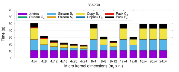
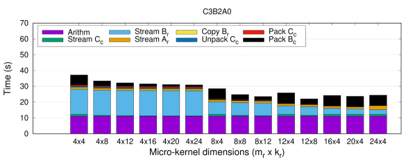
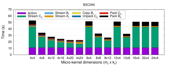
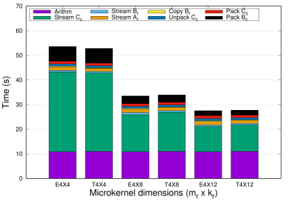
In this section we evaluate the three algorithmic variants for gemm discussed earlier: B3A2C0, C3B2A0 and B3C2A0, comparing their estimated performance as a function of the dimension of the internal micro-kernel ( for the first variant; and for last two), and initially leveraging the same problem case from the previous section: . The size of the selected micro-kernels was determined following the assumptions on the width of the SIMD arithmetic unit (32 bits) and number of vector registers (32) made in Section 3.
Figure 5 shows the distribution of the arithmetic and data/transfer costs, for the three variants, using the performance simulator calibrated for the GAP8 platform. An assumption of our basic simulator is that the arithmetic rate is independent of the micro-kernel dimension and this results in all cases reporting the same cost due to arithmetic. (This assumption may be reasonable for very simple IoT processor designs, but we will discuss this aspect further at the end of this section.) In contrast, for this particular gemm shape, the distribution of costs and the global execution time is highly dependent on the algorithmic variant and micro-kernel dimensions. Thus, for this particular layer of MobileNetV1, both B3A2C0 and B3C2A0 tend to favor “low-and-fat” micro-kernels, such as , while C3B2A0 yields better performance for “squarish” ones: and .
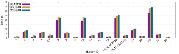
Finally, Figure 6 compares the estimated execution time for the gemm resulting from the application of lowering to all the convolution layers of MobileNetV1. The particular dimensions of these layers are specified in Table 2, together with the optimal micro-kernel dimension for each algorithmic variant and layer dimensions. (Layer #28 is skipped because it does not correspond to a convolution operator.)
The results in this final experiment show that a high variability of the execution time, in accordance with the heterogeneity of the gemm shapes for the distinct layers, but also a general advantage of the B3A2C0 variant. This was not totally unexpected as B3A2C0 mimics the baseline algorithm in BLAS instances such as those in GotoBLAS2, OpenBLAS and BLIS, and presents the advantage of reducing the number of stores in memory during the update of the result . However, we note that this variant depends on the underlying architecture offering an efficient SIMD support for the outer product, which may not be the case for all Iot processors. For example, the GAP8 architecture is especially designed to deliver high performance for the scalar (or dot) product, which favors the gemm variants with resident in the processor registers (C3B2A0 and B3C2A0). This would be reflected in a different (INT8) GOPS rates in our simulator, depending on the type of micro-kernel and architecture design. This architecture-specific adaptation of the simulator to the arithmetic units in the target processor is left as part of future work.
| #Layer ID | B3A2C0 | C3B2A0 | B3C2A0 | |||
|---|---|---|---|---|---|---|
| 1 | 32 | 12544 | 27 | 424 | 244 | 812 |
| 2 | 32 | 12544 | 288 | 424 | 812 | 424 |
| 3 | 64 | 12544 | 32 | 424 | 244 | 128 |
| 4 | 64 | 3136 | 576 | 424 | 128 | 424 |
| 5,7 | 128 | 3136 | 128 | 424 | 244 | 424 |
| 6 | 128 | 3136 | 1152 | 424 | 128 | 424 |
| 8 | 128 | 784 | 1152 | 424 | 128 | 424 |
| 9 | 256 | 784 | 128 | 424 | 244 | 812 |
| 10 | 256 | 784 | 2304 | 424 | 128 | 424 |
| 11 | 256 | 784 | 256 | 424 | 128 | 420 |
| 12 | 256 | 196 | 2304 | 424 | 128 | 424 |
| 13 | 512 | 196 | 256 | 424 | 244 | 424 |
| 14,16,18,20,22 | 512 | 196 | 4608 | 424 | 128 | 424 |
| 15,17,19,21,23 | 512 | 196 | 512 | 424 | 128 | 424 |
| 24 | 512 | 49 | 4608 | 812 | 128 | 424 |
| 25 | 1024 | 49 | 512 | 812 | 128 | 424 |
| 26 | 1024 | 49 | 9216 | 812 | 128 | 424 |
| 27 | 1024 | 49 | 1024 | 812 | 128 | 424 |
| 29 | 1024 | 1000 | 1 | 424 | 244 | 244 |
5 Discussion and Future Work
In order to address the heterogeneous zoo of IoT processor designs for edge computing, we have leveraged a performance simulator for estimating the execution costs of gemm that offers very useful information about which algorithmic variant can better fit a particular architecture.
At the same time, we recognize this work needs to be extended and improved along several paths. As part of future work, we plan to explore several avenues:
-
•
Micro-kernels with or resident in registers are usually cast in terms of distinct assembly SIMD (single instruction, multiple data) instructions. This needs to be taken into account in the calibration experiments.
-
•
Also, most current processors architectures are equipped with DMA controllers. This complicates programming in order to orchestrate asynchronous transfers with computation, and requires double buffering thus reducing the amount of memory for the buffers in the intermediate memory levels.
-
•
Finally, we plan to modify the memory model to take into account actual cache memories instead of scratchpads. This introduces challenges associated with modeling the effects of cache associativity, cache eviction, and replacement policies.
Acknowledgments
This work was supported by the research project PID2020-113656RB-C22 of MCIN/AEI/10.13039/501100011033. C. Ramírez is a “Santiago Grisolía” fellow supported by Generalitat Valenciana. Adrián Castelló is a FJC2019-039222-I fellow supported by MCIN/AEI/10.13039/501100011033. H. Martínez is a “Ayuda Postdoctoral” fellow supported by Consejería de Transformación Económica, Industria, Conocimiento y Universidades de la Junta de Andalucía.
This project has received funding from the European High-Performance Computing Joint Undertaking (JU) under grant agreement No 955558. The JU receives support from the European Union’s Horizon 2020 research and innovation programme, and Spain, Germany, France, Italy, Poland, Switzerland, Norway.
References
- [1] Castelló, A., Igual, F.D., Quintana-Ortí, E.S.: Anatomy of the BLIS family of algorithms for matrix multiplication. In: 30th Euromicro Int. Conf. PDP (2022), to appear
- [2] Goto, K., van de Geijn, R.A.: Anatomy of a high-performance matrix multiplication. ACM Trans. Math. Softw. 34(3), 12:1–12:25 (2008)
- [3] Gunnels, J.A., Gustavson, F.G., Henry, G.M., van de Geijn, R.A.: A family of high-performance matrix multiplication algorithms. In: Proc. 7th Int. Conf. on Applied Parallel Computing. p. 256–265 (2004)
- [4] Hazelwood, K., Bird, S., Brooks, D., Chintala, S., Diril, U., Dzhulgakov, D., Fawzy, M., Jia, B., Jia, Y., Kalro, A., Law, J., Lee, K., Lu, J., Noordhuis, P., Smelyanskiy, M., Xiong, L., Wang, X.: Applied machine learning at Facebook: A datacenter infrastructure perspective. In: IEEE Int. Symp. HPC Architecture. pp. 620–629 (2018)
- [5] Low, T.M., Igual, F.D., Smith, T.M., Quintana-Ortí, E.S.: Analytical modeling is enough for high-performance BLIS. ACM Trans. Math. Softw. 43(2) (2016)
- [6] OpenBLAS. http://xianyi.github.com/OpenBLAS/ (2012)
- [7] Park, J., Naumov, M., Basu, P., Deng, S., Kalaiah, A., Khudia, D., Law, J., Malani, P., Malevich, A., Nadathur, S., Pino, J., Schatz, M., Sidorov, A., Sivakumar, V., Tulloch, A., Wang, X., Wu, Y., Yuen, H., Diril, U., Dzhulgakov, D., Hazelwood, K., Jia, B., Jia, Y., Qiao, L., Rao, V., Rotem, N., Yoo, S., Smelyanskiy, M.: Deep learning inference in Facebook data centers: Characterization, performance optimizations and hardware implications (2018), arXiv 1811.09886
- [8] Ramírez, C., Castelló, A., Quintana-Ortí, E.S.: A BLIS-like matrix multiplication for machine learning in the RISC-V ISA-based GAP8 processor. The Journal of Supercomputing (2022), in review
- [9] Smith, T.M., van de Geijn, R.A.: The MOMMS family of matrix multiplication algorithms. CoRR abs/1904.05717 (2019)
- [10] Sze, V., Chen, Y.H., Yang, T.J., Emer, J.S.: Efficient processing of deep neural networks: A tutorial and survey. Proc. of the IEEE 105(12), 2295–2329 (2017). https://doi.org/10.1109/JPROC.2017.2761740
- [11] Van Zee, F.G., van de Geijn, R.A.: BLIS: A framework for rapidly instantiating BLAS functionality. ACM Trans. Math. Softw. 41(3), 14:1–14:33 (2015)
- [12] Wu, C., Brooks, D., Chen, K., Chen, D., Choudhury, S., Dukhan, M., Hazelwood, K., Isaac, E., Jia, Y., Jia, B., Leyvand, T., Lu, H., Lu, Y., Qiao, L., Reagen, B., Spisak, J., Sun, F., Tulloch, A., Vajda, P., Wang, X., Wang, Y., Wasti, B., Wu, Y., Xian, R., Yoo, S., Zhang, P.: Machine learning at Facebook: Understanding inference at the edge. In: IEEE Int. Symp. HPC Architecture. pp. 331–344 (2019)