Formation of artificial Fermi surfaces with a triangular superlattice on a conventional two dimensional electron gas
Abstract
In nearly free electron theory the imposition of a periodic electrostatic potential on free electrons creates the bandstructure of a material, determined by the crystal lattice spacing and geometry. Imposing an artificially designed potential to the electrons confined in a GaAs quantum well makes it possible to engineer synthetic two-dimensional band structures, with electronic properties different from those in the host semiconductor. Here we report the fabrication and study of a tuneable triangular artificial lattice on a GaAs/AlGaAs heterostructure where it is possible to transform from the original GaAs bandstructure and Fermi surface to a new bandstructure with multiple artificial Fermi surfaces simply by altering a gate bias. For weak electrostatic potential modulation magnetotransport measurements reveal quantum oscillations from the GaAs two-dimensional Fermi surface, and classical oscillations due to these electrons scattering from the artificial lattice. Increasing the strength of the modulation reveals new quantum oscillations due to the formation of multiple artificial Fermi surfaces, and ultimately to new classical oscillations of the electrons from the artificial Fermi surface scattering from the superlattice modulation. These results show that low disorder gate-tuneable lateral superlattices can be used to form artificial two dimensional crystals with designer electronic properties.
Australian Research Council Centre of Excellence in Future Low-Energy Electronics Technologies, University of New South Wales, Sydney 2052, Australia \alsoaffiliationAustralian Research Council Centre of Excellence in Future Low-Energy Electronics Technologies, University of New South Wales, Sydney 2052, Australia \alsoaffiliationAustralian Research Council Centre of Excellence in Future Low-Energy Electronics Technologies, University of New South Wales, Sydney 2052, Australia \altaffiliationPresent Address: Department of Electronic and Electrical Engineering, The University of Sheffield, Mappin Street, Sheffield, S1 3JD, United Kingdom \alsoaffiliationAustralian Research Council Centre of Excellence in Future Low-Energy Electronics Technologies, University of New South Wales, Sydney 2052, Australia \alsoaffiliationAustralian Research Council Centre of Excellence in Future Low-Energy Electronics Technologies, University of New South Wales, Sydney 2052, Australia
The field of 2D materials has received a significant boost with the advent of Moiré superlattices 1. Stacking two atomically thin materials on top of each other with a twist angle between them creates an additional long range potential modulation – the Moiré superlattice. The twist angle between the 2D layers defines the period of the Moiré superlattice, modifying the energy bands and hence the optoelectronic properties. A spectacular example is the case of two single layer graphene sheets stacked on top of each other with a twist angle of 1.08 degrees 2, called magic angle twisted bilayer graphene. The electronic properties of this system can be tuned from a correlated insulator into a superconductor just by changing a gate voltage 3. The origin of this extraordinary behaviour is strong electron-electron interactions due to a flat band formed in the energy spectrum induced by the Moiré superlattice at this very specific twist angle 4. Since the original discovery, other “twisted” 2D material systems have been shown to form flat bands with a variety of correlated phases, making twisted 2D systems the ideal playground to study these exotic electronic phases 5, 6. However, Moiré superlattices have some limitations: 1) the symmetry of the Moiré superlattice is set by the constituent 2D materials; 2) the strength of the periodic superlattice potential is fixed by the interaction between the two 2D layers and cannot be varied; 3) the Moire superlattice requires accurate control of the twist angle between the two layers 2, 3, 7, but very often the fabrication process results in a spatially varying twist angle and thus a spatially non-uniform superlattice 8.
One approach to overcome the limitations of twisted Moiré systems is to use nanolithographically patterned lateral superlattices 9, 10, 11. This technique allows complete control over the lattice symmetry, lattice constant, and strength of the 2D periodic lattice potential. It can also be easily integrated into conventional semiconductor heterostructures, which have the advantage of well-established fabrication technology and superb device quality. Early studies of one-dimensional lateral superlattices in semiconductor heterostructures resulted in the observation of commensurability oscillations in the longitudinal resistance, when the cyclotron orbit of electrons matches the lattice spacing of the artificial 1D lattice 12, 13, and culminated with signatures of Hofstadter physics in the longitudinal and Hall resistances of 2D lateral superlattices 14, 15, 16. However, limitations of materials and fabrication technologies, such as disorder in the patterned superlattice and the weak strength of the lateral superlattice potential, prevented the study of bandstructures in 2D artifical crystals.
The difficulty of creating artificial bandstructures in such a system lies in fabricating an extremely uniform and small-period superlattice while maintaining low disorder(high electron mobility). Both disorder in the patterned superlattice and in the heterostructure can impede the observation of artificial bands. Besides nanofabrication requirements for superlattice patterning (the superlattice period should be or less), modulation-doped heterostructures should also be avoided to suppress long-range charge disorder due to the existence of randomly positioned ionised dopants 17. Furthermore, the energy gap created by a periodic modulation potential is directly related to the strength of the potential, which decays exponentially as a function of the distance between the superlattice and the 2D electron system 18. Therefore, extremely shallow heterostuctures () are essential to achieve a strong enough modulation potential to experimentally observe artificial bandstructure.
Here we overcome these challenges by combining a recently developed ultra-shallow high-mobility 2D electron gas in undoped GaAs/AlGaAs heterostructures with high resolution electron beam lithography, to create an artificial two-dimensional crystal with a gate-tunable 2D lateral superlattice.
A typical device structure in our study is shown in Figure 1(a). The shallow GaAs/AlGaAs accumulation-mode heterostructure is completely undoped and consists of a GaAs buffer, of AlGaAs and a GaAs cap. The 2DEG has a mobility of and a mean free path of at a density of . A thin layer of Ti is deposited on top of the heterostructure and patterned with a triangular array of holes with a lattice constant of and a hole diameter of . This perforated gate is used to induce carriers at the hetero-interface and tune the carrier concentration. A dielectric is then grown on the Ti gate, followed by an overall Ti/Au top gate. The top gate is used to vary the strength of the modulation potential since it is fully screened by the perforated Ti gate except where the holes are. This double-layer design allows both the carrier density and the modulation strength to be varied separately 19.
When a periodic modulation potential is applied to the 2DEG, the parabolic energy bands of free electrons are shifted by a multiple of the reciprocal lattice vector , where is the lattice constant of the periodic modulation. Therefore, the Fermi surface reconstructs into a set of intersecting rings of radius , plotted in blue in Figure 1(b) for a one-dimensional lattice. When the strength of the potential modulation is increased, energy gaps open where these rings intersect, and the topology of the Fermi surface changes into a closed elliptical Fermi surface and open Fermi surface as shown in Figure 1(c). The restructured Fermi surface for a two dimensional triangular lattice is shown in Figure 1(d). Here, the circular shape of the original Fermi surface is evident, but the actual Fermi surface is made up of non-circular closed orbits (black lines in Figure 1(d)), which are separated by energy gaps. In the presence of a weak magnetic field, more complicated trajectories can form when electrons undergo quantum tunnelling from one orbit to another (Figure 1(d)), a process know as magnetic breakdown 20. Any closed trajectories obtained from sections of the original circular Fermi surface linked by quantum tunnelling become a new reconstructed Fermi surface which can quantise and form discrete energy levels. These levels cause quantum (Shubnikov-de Haas) oscillations of the magnetoresistance in an unpatterned 2DEG with a frequency proportional to the area of the orbit and are commonly used to measure the area of the circular Fermi surface. Therefore, the existence of reconstructed Fermi surfaces can also be detected via quantum oscillations of different frequencies.
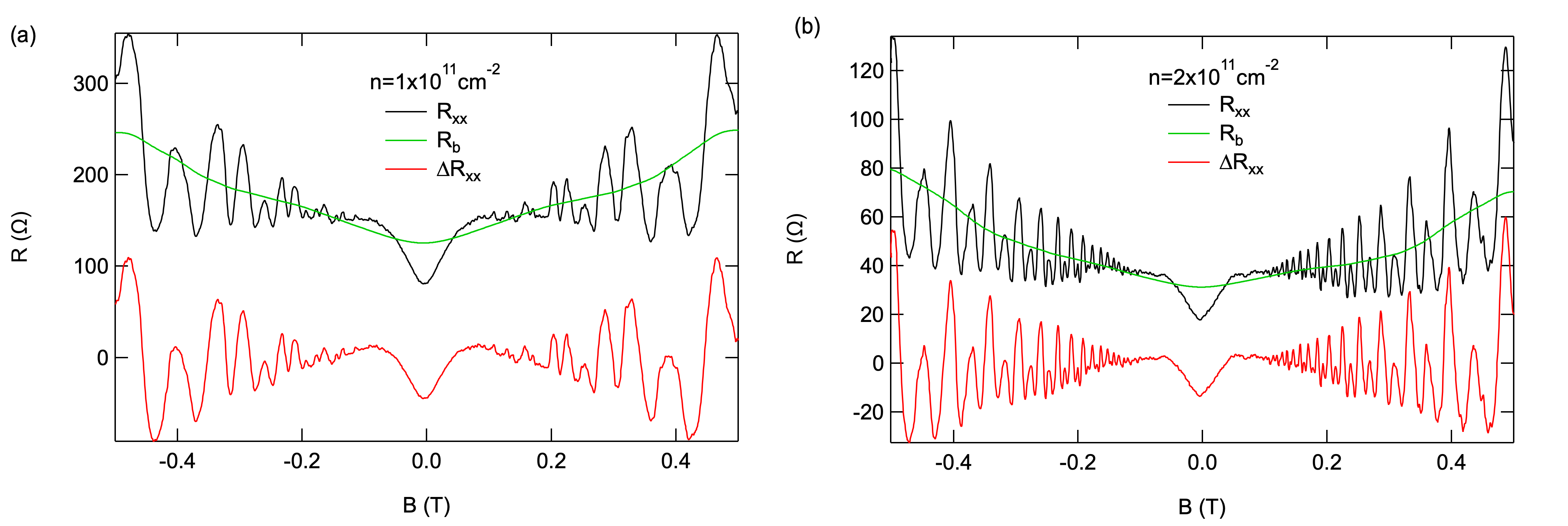
Figure 2(a) shows the experimentally measured magnetoresistance of the device, as a function of the carrier density, , and the perpendicular magnetic field, , at . A smoothed background is removed from to make the magnetoresistance oscillations in more visible (See supplementary S1 for details). In Figure 2, is set to which corresponds to a weak modulation potential. At this modulation strength, shows a complicated braiding pattern signalling the existence of oscillations at different frequencies. To extract the individual frequency components the Fourier transform of is computed. The amplitude of the frequency components is plotted in logarithmic colour scale in Figure 2(b), where large amplitude appears as dark blue. As shown in Figure 2(b), multiple frequency components can be clearly identified over a wide density range.
To understand the origin of these different frequency components, the same measurement is repeated at a higher temperature of . At , all low-field quantum oscillations are suppressed due to thermal excitation, leaving only classical oscillations. Figures 2(c) and (d) plot and the Fourier transform of at respectively. The two frequency components in Figure 2(d) which also exist at are highlighted by the grey dashed lines in Figure 2(b). These two frequency components are caused by classical commensurability oscillations. In a semi-classical picture, the drift velocity perpendicular to the lattice plane vanishes when the cyclotron orbit is commensurate with the distance between lattice planes (Figure 3(a)), resulting in resistance minima 21. This commensurability occurs when the cyclotron radius is related to the spacing between lattice planes by
| (1) |
where is an integer. Substituting , it can be easily shown that commensurability oscillations are periodic in with a periodicity of
| (2) |
which are the grey dashed lines plotted in Figure 2(b).
For a 2D triangular superlattice with lattice constant , the spacing between the fundamental set of lattice planes is (Figure 3(a)). The frequency calculated from Eq.(2), CO1, is plotted as the red dashed line in Figure 2(d) and is in excellent agreement with the experiment with no fitting parameters. The locations of resistance minima are also very well predicted by Eq. (1), shown as the red dashed lines in Figure 2(c). The other frequency component highlighted by the orange dashed line in Figure 2(d), CO2, corresponds to a new commensurate condition that is unique to the 2D triangular superlattice. Due to the symmetry of the triangular lattice, consecutive lattice planes are not equivalent. From one plane to the next there is a horizontal shift of the lattice sites by . This feature of the the 2D triangular superlattice gives rise to another set of lattice planes with spacing . Thus, two sets of commensurability oscillations are observed in the experiment with one having exactly half the frequency of the other.
Excluding these commensurability oscillations, the remaining frequency components in Figure 2(b) have a strong temperature dependence and are only visible at low temperatures. They are quantum oscillations arising from different Fermi surfaces. The frequency of quantum oscillations from a closed Fermi surfaces is related to the area of the Fermi surface through
| (3) |
where is the area of the Fermi surface. The area of the reconstructed Fermi surfaces can be calculated geometrically using the original circular Fermi surface, whose radius is (where is the electron density). From the experimental data, we identify three different Fermi surfaces , and as depicted in Figure 3(b). The calculated frequencies of the quantum oscillations from these Fermi surfaces are plotted as red, blue and green dashed lines in Figure 2(b) and are in excellent agreement with the experiment.
The observation of reconstructed Fermi surfaces and is strongly related to the process of magnetic breakdown. The probability of electrons completing loops around different Fermi surfaces depends on their probability of tunnelling through the energy gap at the anticrossing between different Brillouin zones (Figure 1(d)). For a weak magnetic field , the tunnelling probability is proportional to the size of the gap, which is directly related to the strength of the electrostatic modulation from the periodic lattice. If the modulation is not too strong, the gap is small and the tunnelling probability is high. Therefore, only Fermi surfaces and with two reflections, the minimum number of reflections required to define a reconstructed Fermi surface, are observed experimentally. The higher visibility of compared to in Figure 2(b) can be understood by the shorter real space trajectory of than . This means electrons are more likely to complete orbits defined by rather than , which makes the main reconstructed Fermi surface in the system.
The process of magnetic breakdown also explains the braiding pattern of in Figure 2(a). At large magnetic fields, tunneling probability is high and the original Fermi surface is fully restored due to magnetic breakdown. Therefore, at magnetic fields larger than , only the Landau fan of states associated with are visible. At lower magnetic fields, , magnetic breakdown becomes weak and electrons start to follow the reconstructed Fermi surface . Unlike , the Landau fan of emanates from a finite electron density of . This is the electron density at which , the radius of , is equal to the reciprocal lattice vector and thus the density where begins to form. The co-existence of the and Landau fans at intermediate fields results in the braiding pattern in as illustrated by the calculated fan diagram in Figure 3(c).
There are two additional frequency components (indicated by black arrows in Figure 2(b)) which similarly to the and lines, disappear at . Their frequencies correspond to fractional combinations of the and lines, i.e. and . These frequencies can also be interpreted as averages: is the average of and while is the average of and . Neither nor can be understood as arising from closed Fermi surface trajectories with area or since no such trajectories exists in the triangular lattice Fermi surface. Lines with these frequencies have not been observed before in 1D 15 or 2D lattices 14 and are not currently understood.
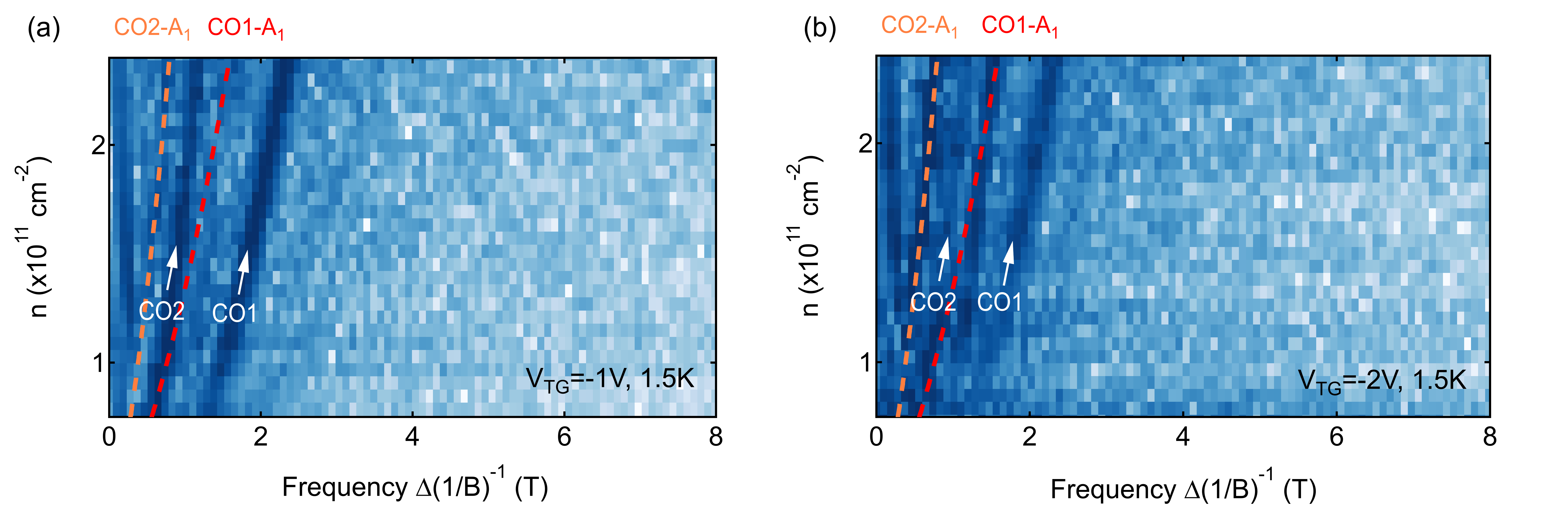
Finally we examine how the system behaves when the modulation strength is increased. Increasing the negative bias on the top-gate strengthens the modulation potential. Figure 4(a) shows the Fourier transform of background removed magnetoresistance at as a function of for . Comparing Figure 2(b) at to Figure 4(a) at , two extra frequency components are observed and highlighted by the dashed lines labelled CO1-A1 and CO2-A1. We trace these frequencies to the commensurability oscillations of the reconstructed Fermi surface (see supplementary section 0.3 for more details). As shown in Figure 3(b), the formation of only requires lattice planes in one dimension. Therefore, for a 2D triangular lattice, electrons from Fermi surface can scatter from the other two sets of lattice planes, at giving rise to commensurability oscillations of the reconstructed Fermi surface as shown in Figure 4(b). The calculated frequency of this commensurate condition of (see supplementary section 0.1) is plotted as the red dashed line in Figure 4(a) labelled CO1-A1. Unique to the triangular lattice, every second lattice plane can give rise to another set of commensurability oscillations of the reconstructed Fermi surface as shown in Figure 4(c). This double spacing condition thus produces commensurability oscillations at a frequency exactly half of CO1-A1, which is plotted as the orange dashed line labelled CO2-A1 in Figure 4(a). The calculated frequencies of both CO1-A1 and CO2-A1 are in excellent agreement with the experiment, again with no fitting parameters.
In conclusion, we observe oscillations in magnetoresistance that are unambiguously linked to the artificial bandstructure due to a 2D lateral superlattice. Furthermore, as we increase the modulation potential we observe, for the first time, the classical commensurability oscillations of the reconstructed Fermi surface at elevated temperatures. Our work demonstrates a path to bandstructure engineering in conventional semiconductor systems, which could open new opportunities towards studying the physics of artificial graphene, strongly correlated systems, superconductivity and magnetism, as well as artificial 2D topological insulators 22, 23, 24, 25.
This work was funded by the Australian Research Council Centre of Excellence for Future Low Energy Electronics Technologies (CE170100039) and EP/R029075/1 Non-Ergodic Quantum Manipulation, UK. Device fabrication was partially carried out at the Australian National Fabrication Facility (ANFF) at the UNSW node.
0.1 Calculation of frequency lines in the Fourier transform of magnetoresistance oscillations
There are two kinds of frequency lines that we compute: there are the quantum oscillations which come from Onsager’s formula, and there are commensurability oscillations which come from a generalisation of the standard commensurability condition. Both of these kinds of frequencies depend on the geometry of the Fermi surface: the quantum frequencies are proportional to the area of the orbit, and the commensurability frequencies are proportional to the width of the orbit in a particular direction. In all of these calculations it is sufficient to compute the area in the limit that the modulation strength goes to zero. For the quantum oscillations, the areas of and are given by
The equation for is the area of intersection between two circles of radius and separation . The frequencies , , and , plotted in Figure 2, can then be obtained using equation Eqn. 3.
Commensurability frequencies come from comparing the width of an orbit in real space to a certain set of lattice planes. For the standard commensurability oscillations (CO1 in Fig. 3a) we are comparing the width, , of to the spacing between lattice planes, , to obtain a frequency
Where is the width of the orbit in -space. This is equivalent to equation Eqn. 2. The frequency of CO2 (see Fig. 3a) is then obtained by doubling the lattice plane spacing to , which halves the frequency. More general frequencies are obtained by comparing the width of in real space to the set of lattice planes that make a 30 degree angle with the major axis of . This was depicted in Fig. 4b. The real space width, , is the total width of the orbit along a line perpendicular to the lattice planes, that is, a line making a 60 degree angle to the major axis of . In -space this width turns out to be equal to
And, with , we obtain a frequency
0.2 Background removal of
In the main text, background removed longitudinal resistance is plotted instead of to emphasize the resistance oscillations. is also used in the Fourier analysis. In Figure S1 we show the original , the smoothed background and the resultant for two different densities.
0.3 The effect of temperature on COs of the Fermi surface
To identify the origin of new oscillations when the modulation strength is increased, magnetoresistance measurements and subsequent Fourier analysis are performed at an elevated temperature of . As shown in Figure S2(a), at the same modulation strength as in Figure 4(a), new frequency components (CO1-A1 and CO2-A1) become very weak at . However, if the modulation strength is increased further to , CO1-A1 and CO2-A1 persist to higher temperatures as can be seen in Figure S2(b). The existence of these frequency components at strongly suggests that they originate from classical commensurability oscillations, although a stronger modulation potential is required to observe them. This is because thermal excitation increases the probability of electrons tunnelling through the energy gap between different orbits and thus prohibits the formation of the reconstructed Fermi surface . Therefore, a stronger modulation potential (i.e. larger energy gap) is required to observe the commensurability oscillations of at elevated temperatures.
References
- Dean et al. 2013 Dean, C.; Wang, L.; Maher, P.; Forsythe, C.; Ghahari, F.; Gao, Y.; Katoch, J.; Ishigami, M.; Moon, P.; Koshino, M.; Taniguchi, T.; Watanabe, K.; Shepard, K.; Hone, J.; Kim, P. Hofstadter’s butterfly and the fractal quantum Hall effect in moire´ superlattices. Nature 2013, 497, 598–602
- Cao et al. 2018 Cao, Y.; Fatemi, V.; Demir, A.; Fang, S.; Tomarken, S. L.; Luo, J. Y.; Sanchez-Yamagishi, J. D.; Watanabe, K.; Taniguchi, T.; Kaxiras, E.; Ashoori, R. C.; Jarillo-Herrero, P. Correlated insulator behaviour at half-filling in magic-angle graphene superlattices. Nature 2018, 556, 80–84
- Cao et al. 2018 Cao, Y.; Fatemi, V.; Fang, S.; Watanabe, K.; Taniguchi, T.; Kaxiras, E.; Jarillo-Herrero, P. Unconventional superconductivity in magic-angle graphene superlattices. Nature 2018, 556, 43–50
- Bistritzer and MacDonald 2011 Bistritzer, R.; MacDonald, A. Moiré bands in twisted double-layer graphene. Proc. Natl Acad. Sci. 2011, 108, 12233–12237
- Liu et al. 2020 Liu, X.; Hao, Z.; Khalaf, E.; Lee, J. Y.; Ronen, Y.; Yoo, H.; Haei Najafabadi, D.; Watanabe, K.; Taniguchi, T.; Vishwanath, A.; Kim, P. Tunable spin-polarized correlated states in twisted double bilayer graphene. Nature 2020, 583, 221–225
- Wang et al. 2020 Wang, L. et al. Correlated electronic phases in twisted bilayer transition metal dichalcogenides. Nature Materials 2020, 19, 861–866
- Lu et al. 2019 Lu, X.; Stepanov, P.; Yang, W.; Xie, M.; Aamir, M. A.; Das, I.; Urgell, C.; Watanabe, K.; Taniguchi, T.; Zhang, G.; Bachtold, A.; MacDonald, A. H.; Efetov, D. K. Superconductors, orbital magnets and correlated states in magic-angle bilayer graphene. Nature 2019, 574, 653–657
- Uri et al. 2020 Uri, A.; Grover, S.; Cao, Y.; Crosse, J. A.; Bagani, K.; Rodan-Legrain, D.; Myasoedov, Y.; Watanabe, K.; Taniguchi, T.; Moon, P.; Koshino, M.; Jarillo-Herrero, P.; Zeldov, E. Mapping the twist-angle disorder and Landau levels in magic-angle graphene. Nature 2020, 581, 47–52
- Forsythe et al. 2018 Forsythe, C.; Zhou, X.; Watanabe, K.; Taniguchi, T.; Pasupathy, A.; Moon, P.; Koshino, M.; Kim, P.; Dean, C. R. Band structure engineering of 2D materials using patterned dielectric superlattices. Nature Nanotechnology 2018, 13, 566–571
- Jessen et al. 2019 Jessen, B. S.; Gammelgaard, L.; Thomsen, M. R.; Mackenzie, D. M. A.; Thomsen, J. D.; Caridad, J.; Duegaard, E.; Watanabe, K.; Taniguchi, T.; Booth, T. J.; Pedersen, T. G.; Jauho, A.-P.; Bøggild, P. Lithographic band structure engineering of graphene. Nature Nanotechnology 2019, 14, 340–346
- Huber et al. 2022 Huber, R.; Steffen, M. N.; Drienovsky, M.; Sandner, A.; Watanabe, K.; Taniguchi, T.; Pfannkuche, D.; Weiss, D.; Eroms, J. Band conductivity oscillations in a gate-tunable graphene superlattice. Nature Communications 2022, 13, 2856
- Gerhardts et al. 1989 Gerhardts, R. R.; Weiss, D.; Klitzing, K. v. Novel magnetoresistance oscillations in a periodically modulated two-dimensional electron gas. Phys. Rev. Lett. 1989, 62, 1173–1176
- Winkler et al. 1989 Winkler, R. W.; Kotthaus, J. P.; Ploog, K. Landau band conductivity in a two-dimensional electron system modulated by an artificial one-dimensional superlattice potential. Phys. Rev. Lett. 1989, 62, 1177–1180
- Albrecht et al. 1999 Albrecht, C.; Smet, J. H.; Weiss, D.; von Klitzing, K.; Hennig, R.; Langenbuch, M.; Suhrke, M.; Rössler, U.; Umansky, V.; Schweizer, H. Fermiology of Two-Dimensional Lateral Superlattices. Phys. Rev. Lett. 1999, 83, 2234–2237
- Deutschmann et al. 2001 Deutschmann, R. A.; Wegscheider, W.; Rother, M.; Bichler, M.; Abstreiter, G.; Albrecht, C.; Smet, J. H. Quantum Interference in Artificial Band Structures. Phys. Rev. Lett. 2001, 86, 1857–1860
- Geisler et al. 2004 Geisler, M. C.; Smet, J. H.; Umansky, V.; von Klitzing, K.; Naundorf, B.; Ketzmerick, R.; Schweizer, H. Detection of a Landau Band-Coupling-Induced Rearrangement of the Hofstadter Butterfly. Phys. Rev. Lett. 2004, 92, 256801
- Srinivasan et al. 2020 Srinivasan, A.; Farrer, I.; Ritchie, D. A.; Hamilton, A. R. Improving reproducibility of quantum devices with completely undoped architectures. Applied Physics Letters 2020, 117, 183101
- Tkachenko et al. 2015 Tkachenko, O. A.; Tkachenko, V. A.; Terekhov, I. S.; Sushkov, O. P. Effects of Coulomb screening and disorder on an artificial graphene based on nanopatterned semiconductor. 2D Materials 2015, 2, 014010
- Wang et al. 2020 Wang, D. Q.; Reuter, D.; Wieck, A. D.; Hamilton, A. R.; Klochan, O. Two-dimensional lateral surface superlattices in GaAs heterostructures with independent control of carrier density and modulation potential. Applied Physics Letters 2020, 117, 032102
- Steda and MacDonald 1990 Steda, P.; MacDonald, A. H. Magnetic breakdown and magnetoresistance oscillations in a periodically modulated two-dimensional electron gas. Phys. Rev. B 1990, 41, 11892–11898
- Beenakker 1989 Beenakker, C. W. J. Guiding-center-drift resonance in a periodically modulated two-dimensional electron gas. Phys. Rev. Lett. 1989, 62, 2020–2023
- Park and Louie 2009 Park, C.-H.; Louie, S. Making Massless Dirac Fermions from a Patterned Two-Dimensional Electron Gas. Nano Letters 2009, 9, 1793–1797
- Sushkov and Castro Neto 2013 Sushkov, O. P.; Castro Neto, A. H. Topological Insulating States in Laterally Patterned Ordinary Semiconductors. Phys. Rev. Lett. 2013, 110, 186601
- Du et al. 2021 Du, L.; Liu, Z.; Wind, S.; Pellegrini, V.; West, K.; Fallahi, S.; Pfeiffer, L.; Manfra, M.; Pinczuk, A. Observation of Flat Bands in Gated Semiconductor Artificial Graphene. Physical Review Letters 2021, 126, 106402
- Polini et al. 2013 Polini, M.; Guinea, F.; Lewenstein, M.; Manoharan, H. C.; Pellegrini, V. Artificial honeycomb lattices for electrons, atoms and photons. Nature Nanotechnology 2013, 8, 625