Understanding the band offset between materials is pivotal for electronic device functionality. While traditional theories attribute this offset solely to intrinsic properties of constituent materials, interfacial chemistry introduces complexities, including charge transfer dipoles. We address this challenge by defining a reference system based on Wigner-Seitz atoms, which is a charge partitioning that tessellates space while retaining bulk crystal symmetry. The interfacial dipole is then expressed entirely by localized dipoles along interfacial bonds. Geometric analysis reveals that for isotropic materials, both bulk and interfacial contributions to the band offset are orientation independent. This finding is confirmed through first-principles calculations and analysis of 28 distinct interfaces, which show very little ( 0.1 eV) dependence on orientation. Furthermore, the direction dependence of anisotropic materials is well captured by the theory. This work provides crucial insights into the geometric underpinnings of band offset, offering a comprehensive understanding essential for advancing materials design in electronic applications.
Bond Dipole Theory of Band Offset
I Introduction
With the rise of micro and quantum electronics, understanding the interface at the atomic level can be critically important for the semiconductor industry[1, 2, 3, 4, 5]. Of key importance to interface electronics is the band offset which determines the performance threshold of quantum devices[6, 7, 8, 9, 10]. Since the 1980s, a wide number of experiments[11, 12, 13, 14, 15] have revealed that the band offset of conventional semiconductors are largely independent of interface orientation. These results are quite surprising given that different orientations are associated with different concentrations of interfacial bonds and defects, and hence the interfacial charge transfer (and the resulting interfacial dipole) contribution to the band offset is expected to depend strongly on the interfacial details. How the bulk and interfacial properties of heterostructures conspire to yield nearly orientation independent band offsets remains a deep mystery.
On the theoretical side, first-principles methods like density functional theory (DFT) can provide fully quantum mechanical treatment of the band offset of specified materials using a periodic supercell containing an atomically constructed interface[16, 17, 18, 19, 20, 21]. These calculations provide high quality results and reproduce the experimentally observed orientation independence. However, as such approaches merely output the self-consistent ground state electronic configuration of the interface, they provide very limited insight into the underlying physics of interface formation. Nevertheless, from such calculations, it is clear that the dipole formation which governs the band offset is quite local in nature (typically on the order of a bond length) and can be adequately described in supercells an order of magnitude smaller than is needed to describe many fully quantum mechanical phenomena[22, 23].
One of the most famous examples to understand band offset is the Anderson’s rule[24] which proposes that two isolated semiconductors are aligned through their workfunctions. Typically, Anderson’s rule works well for van der Waals-coupled low dimensional systems[25] but fails in covalent systems as the assumption is esstentially that no charge rearrangement takes place when the two systems are brought together, which would lead to a dipole at the interface. Further, this highlights the fundamental issue that the local interfacial relaxation dipole can only be defined with respect to a reference configuration, and it is unclear what reference system can provide the most physical insight.
Considerable efforts[26, 27, 28, 16] have been made to separate the bulk contributions and clarify the mechanism of interfacial dipole relaxation. However, while such studies agree on the band offset, different choices of reference lead to strongly conflicting values for the contribution of the interfacial dipole. While some methods, such as superposition of atomic charge, sucessfully remove orientation dependence of the bulk contribution to band offset, they do not accurately respresent the bulk charge densities of the constiuent materials and are hence difficult to justify. Furthermore, little light is shed on the interfacial charge transfer dipole and the physical mechanism by which it becomes direction independent.
Quite another approach was proposed by Tersoff in Ref.[29, 30], wherein the band offset is enitrely a property of the individual bulk materials. Instead of determining charge transfer at the interface, the bulk band structures of two semiconductors are said to be aligned at their respective charge neutrality levels. While this branch point theory is widely cited to understand orientation independence of the interface properties, there exist multiple conflicting definitions of the charge neutrality level in the literature[31, 32, 33] and its validity is difficult to experimentally access. A perspicuous theory of interface physics with explicit separation between bulk and interfacial contributions, at even the level, is largely lacking.
In this work, we use real space partitioning of the bulk charge density consisting of ion-centered charge neutral polyhedra, dubbed Wigner-Seitz atoms, to formulate a theory of the band offset of solids. This construction allows a clear separation between the bulk contribution to the band offset, involving the bulk quadrupole, and subsequent charge relaxation leading to an interfacial charge transfer dipole (interfacial dipole). Using density functional theory (DFT) we examine the interface of isotropic systems including cubic, diamond, zincblende, rock-salt, and cadmium chloride lattices in three dimensions (3D) and square, triangular, and hexagonal lattices in two dimensions (2D). Here, we find that the valence band offset (VBO) can be largely explained by the orientation independent bulk quadrupole contribution, with the interfacial dipole contribution being only on the order of 0.4 eV (in terms of root-mean-square value). Furthermore, we find that the interfacial dipole can be understood almost entirely in terms of the sum of local bond dipoles which form along the individual interfacial bonds. A general classical model for the interfacial dipole, in terms of the local bond dipoles, is constructed and allows for determination of the band offset for an interface of arbitrary orientation. This model is used to successfully describe the direction dependent band offset between anisotropic AlN and GaN. Further, application to the interface between isotropic monoatomic systems and between binaries which share a common anion/cation, reveals that as a consequence of the underlying geometry, the interfacial dipole and hence the VBO become entirely direction independent. The unearthing of the local nature of the interfacial dipole and its success in describing the band offset demonstrate the utility of the Wigner-Seitz charge partitioning.
II Results and Discussion
II.1 Wigner-Seitz atom and solid
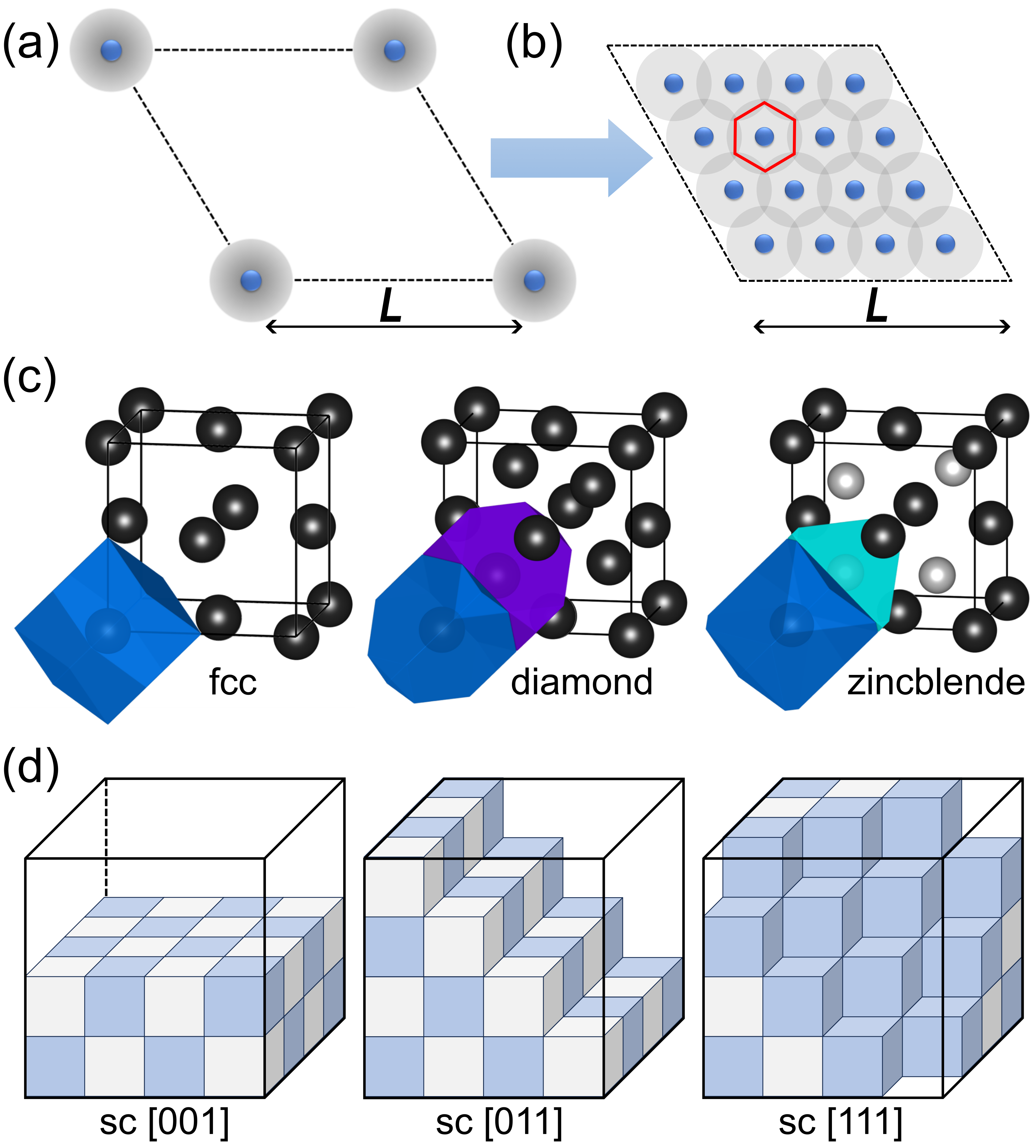
The formation of an interface has two steps: (1)A surface is truncated from periodic bulk with fixed charge density and the two truncated surfaces are merged into an interface, (2)Interface dipoles are formed when the truncated charge density at the interfaces relaxes to equilibrium. The former dominates the bulk contribution to band offset while the latter is the interface effect which provides an additional potential shift across the interface. As a prerequisite, the truncation must avoid any macroscopic fields in order to preserve the crystal translational symmetry as well as the local symmetry of atoms. For atoms which are far separated, as in Fig. 1 (a), the charge density can be considered spherical and directly associated with a particular ion, however, as the spacing is decreased to form a solid, as in Fig. 1 (b), the charge densities of adjacent atoms overlap, lowering the local atomic symmetry to that of the crystal as shown by the red hexagon. Due this overlap, restoring spherical symmetry of the atomic charge is neither well defined, nor can be accomplished through real-space charge truncation. Instead, reminiscent of the concept of Wigner-Seitz unit cell[34] which reassigns the volumes of crystal into atom-centered polyhedrons, we partition the atomic charge to respect the crystal symmetry.
Wigner-Seitz unit cell is defined for Bravais lattices, however, for a composite lattice which has multiple atoms in each unit cell, the volume of Wigner-Seitz unit cell has to be further decomposed into even smaller polyhedrons centered on each atom[35]. Such atom-specific polyhedron, here dubbed as Wigner-Seitz atom, refer to the volume contained within the cutting planes which are perpendicular to the lines connecting neighboring atoms in which the cutting plane distance along the line is determined by the requirement of charge neutrality. As exemplified in Fig. 1(c), the Wigner-Seitz unit cell of face-centered cubic (fcc) lattice is a rhombic dodecahedron, while the Wigner-Seitz atom of diamond structure is a triakis truncated tetrahedral honeycomb[36]. More generally, the volume of Wigner-Seitz atom will be element-specific for a compound due to the varied electron affinities of different species and the required charge neutrality of each individual Wigner-Seitz atom[37], as shown by the zincblende structure in Fig. 1(c). By a tessellation of Wigner-Seitz atoms in real space[38, 39], the bulk charge density can be reproduced without any overlap or void, leading to a Wigner-Seitz solid.
II.2 Wigner-Seitz interface
A Wigner-Seitz surface can be defined for any arbitrary direction by partitioning the bulk charge density along the boundaries of Wigner-Seitz atoms, as exemplified for a simple cubic lattice in Fig. 1(d), and a Wigner-Seitz interface is constructed by aligning up two such surfaces without relaxing the interfacial charge. Here we show that the Wigner-Seitz interface is an excellent reference to separate bulk and interfacial contributions to interface formation, since such developed interfacial dipoles are small and more importantly for isotropic systems, it leads to rigorous orientation independence of the band offset.
This can be shown by considering the band offset of the Wigner-Seitz interface before electronic relaxation. To determine the band offset, we first consider the average potential of each material relative to the associated vacuum in the vicinity of the surface (with surface normal ). Here we note this quantity is typically strongly dependent on surface orientation [40, 41, 42] and is given by
| (1) | ||||
where is the unit cell volume, is the electric quadrupole, and is the charge density of Wigner-Seitz atom of -th species (e.g., for binaries). The potential shift is purely determined by the bulk properties and dominates the bulk effect of interface formation. By expanding Eq. (1) we have
| (2) | ||||
where , and are the , and components of normal vector with . The first and second terms on right correspond to the diagonal and off-diagonal elements of the quadrupole tensor. For isotropic systems with equivalent , and axes,
| (3) |
where is the bulk electric quadrupole of -th species. Taking into account the two-fold rotational symmetry along three axes of an isotropic system, the off-diagonal terms in Eq. (2) will vanish. Finally, for isotropic systems Eq. (1) turns out to be
| (4) |
which is rigorously orientation independent. By constructing a Wigner-Seitz interface, the vacuum levels of two Wigner-Seitz surfaces align with each other, leading to an orientation independent band offset between two materials for isotropic systems.
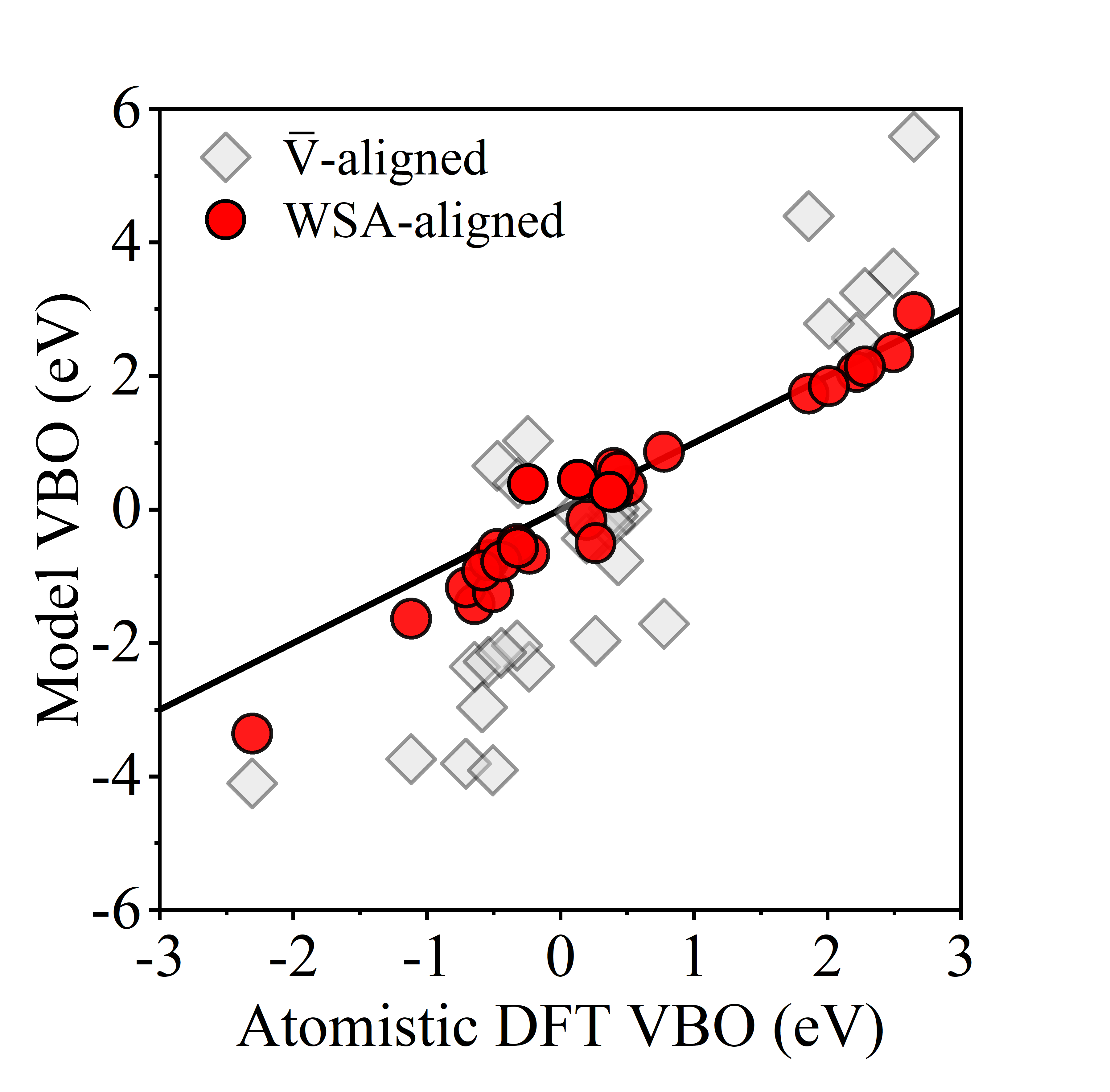
Figure 2 shows the valence band offsets (VBO) obtained from Wigner-Seitz interfaces and atomistic DFT supercell calculations for 28 distinct interfaces of materials with a wide range of structures and properties, including cubic, diamond, zincblende, rock-salt, and cadmium chloride lattices in 3D and square, triangular, and hexagonal lattices in 2D. We see that Wigner-Seitz interface well reproduces the results of atomistic DFT calculations even without interfacial electronic relaxation and only in few cases the developed interfacial dipole reaches up to 1 eV. As comparison, we also give in Fig. 2 the band offsets calculated by aligning the average potential of individual bulks which, despite also being orientation independent, is poorly matched to the atomistic DFT results. By choosing this Wigner-Seitz solid reference, we see that the essential physics of VBO is captured by the bulk properties of the constituent materials and that the interfacial dipole which develops due to charge relaxation is a small contribution to the band offset. In the next section, we will investigate the details of the interfacial dipole and explain why it too is largely orientation independent.
II.3 Interfacial bond dipole
Even when considering the interface between two materials which are lattice matched, the details of the geometry and atomic coordination at the interface depends on its orientation. While the band offset of Wigner-Seitz interface can be rigorously isotropic, the onset of interfacial dipole relaxation could in principle break the symmetry and lead to anisotropic results. However, both experiments and atomistic DFT calculations confirm the orientation independence of band offset in the equilibrium interface, suggesting that the dipole relaxation of Wigner-Seitz interface must also be orientation independent.
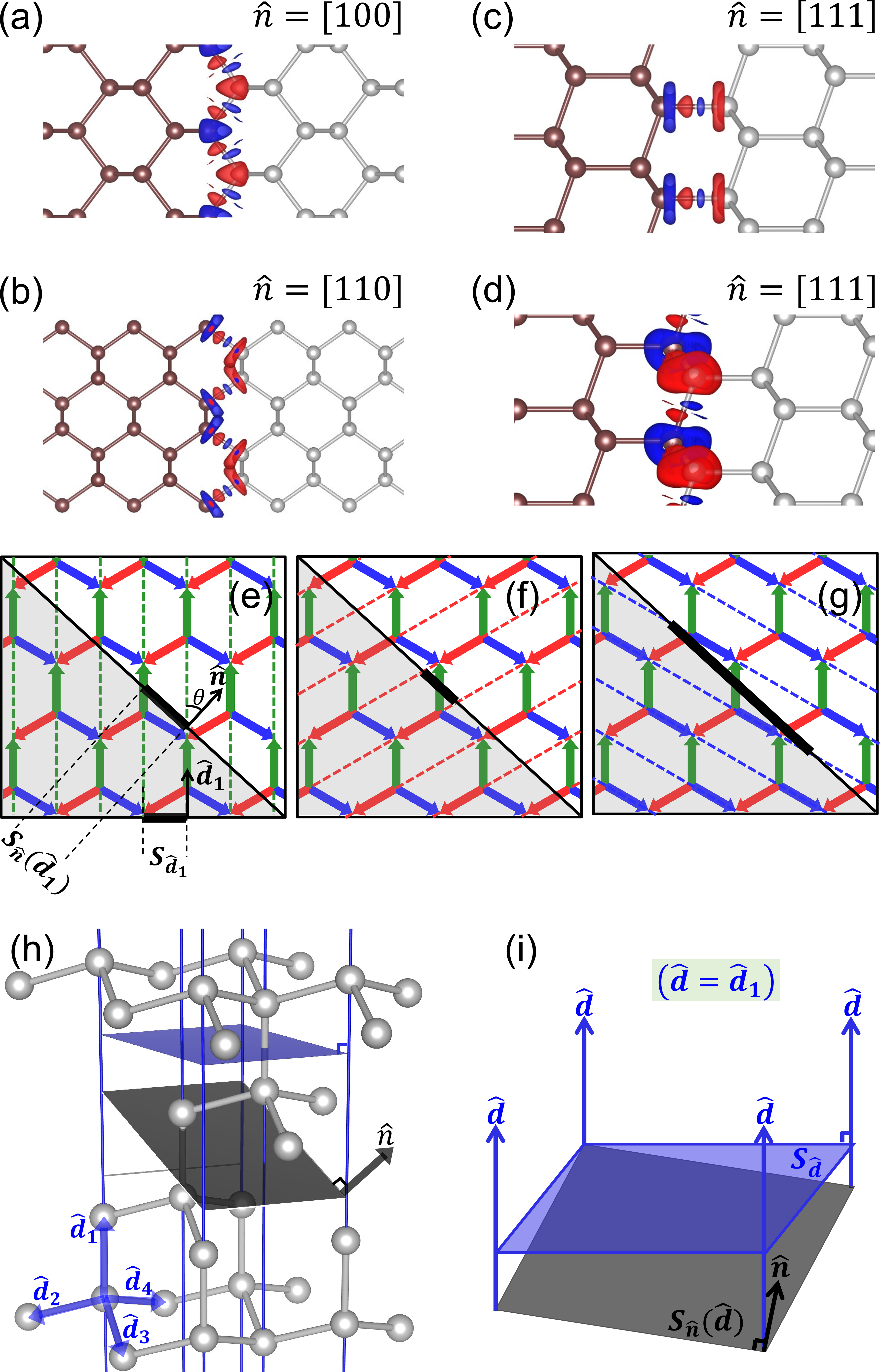
Using the diamond structure Si-Ge as an example of a protypical interface, the charge density associated with the interfacial dipole is depicted in Figs. 3(a-d). We find that the charge relaxation occurs along the bonds across interface. Furthermore, the magnitude of the bond dipole, , is primarily an interatomic property which is only weakly affected by the interface orientation that is calculated to be 26.11 eÅ along the [100] and 26.08 eÅ along the [110]. For the [111] direction, the interface can have one or three interfacial bonds per unit cell area, and is calculated to be 26.13 eÅ and 26.01 eÅ, respectively. Here it is important to distinguish between the bond dipole and the net interfacial dipole perpendicular to the interface which directly contributes to the band offset. The magnitude of the bond dipole is driven by the overlap (or void) between Wigner-Seitz atoms of different species across the interface. However, the contribution of this bond dipole to the band offset explicitly depends on the component normal to the interface. From a simple capacitor model, the potential shift across the interface is
| (5) |
where is the vacuum dielectric constant, is the interface normal direction, and is the interfacial density of bond dipole projected onto the direction,
| (6) |
where is the area per bond in the interface plane.
However, even for the simplest lattices there is more than one bond direction (), and generally the contributions of each type of bond and their orientations at the interface have to be considered, i.e., . We have to sum up the contributions of to calculate the final results of . This is illustrated by a 2D hexagonal lattice in Figs. 3(e-g), where the three s are indicated by arrows in different colors. For each , we define a family of “bond lines” (dashed lines in the same color of ) where each bond of that type falls directly on the lines. For a given bond line, some percentage of the line is occupied by bonds, denoted by the filling factor ( for the 2D hexagonal lattice), with the rest being empty space. The formation of an interface, indicated by the black line, can be seen as the truncation of bulk bond lines which will then be reconnected to a dissimilar material. Here the key point is that each bond line is cut by the interface plane only once, and each bond line, due to , can contribute at most a single interfacial bond (associated with bond dipole ).
In general, to determine the density and orientation of interfacial bond dipoles, we note that each bond line (orientated in ) provides a bond dipole of . Furthermore, we note that even for the same interface normal direction , the area per bond line depends on , e.g., . Putting all these together, the general expression of is
| (7) |
The dependence of on and is most easily seen for the 2D case shown in Figs. 3(e-g). In Fig. 3(e), the bond lines associated with the direction are shown with green dashed lines and the interface in the direction is indicated by the thin solid black line. The length of interface per bond line, , is indicated by the thick solid black line. Here, it can be seen that , where is the perpendicular distance between bond lines. Similarly, and are depicted in Figs. 3(f) and (g), respectively.
This relationship can be straightforwardly generalized to 3D, as shown in Figs. 3(h-i) where the plane perpendicular to the bond lines, , is shown in blue and the interface plane is shown in black. From the orthogonality between and and between and , the general expression for can be written as,
| (8) |
where the angle between and . Thus, has the formula
| (9) |
For isotropic structures as listed in Table. I, , , and are independent of so that , and . For each of the isotropic structures listed in Table. I, straightforwardly performing the summation in Eq. (9) reveals that it becomes independent of interface orientation , simplifying to
| (10) |
where depends on the specific crystal structure, as listed in Table 1, but not on the orientation of the interface.
These results indicate that the interfacial dipole which develops at the interface originates from local dipoles associated with bonds across the interface. For an interface between isotropic monoatomic materials, this leads to an interfacial dipole which is strictly independent of the interface orientation. In general, however, for traditional semiconductors (which are typically binaries, i.e., AX) different types of interfacial bonds exist. Furthermore, surfaces can be A or X terminated, leading to polar interfaces, which is the subject of our next section.
| Lattice | |||||
|---|---|---|---|---|---|
| 3D | simple cubic | 1 | 1 | ||
| body-centered cubic | 1 | ||||
| face-centered cubic | 1 | 2 | |||
| diamond | |||||
| zincblende | |||||
| rock-salt | 1 | 1 | |||
| cadmium chloride | 1 | ||||
| 2D | square | 1 | 1 | ||
| triangular | 1 | ||||
| hexagonal |
II.4 Non-polar and polar interfaces
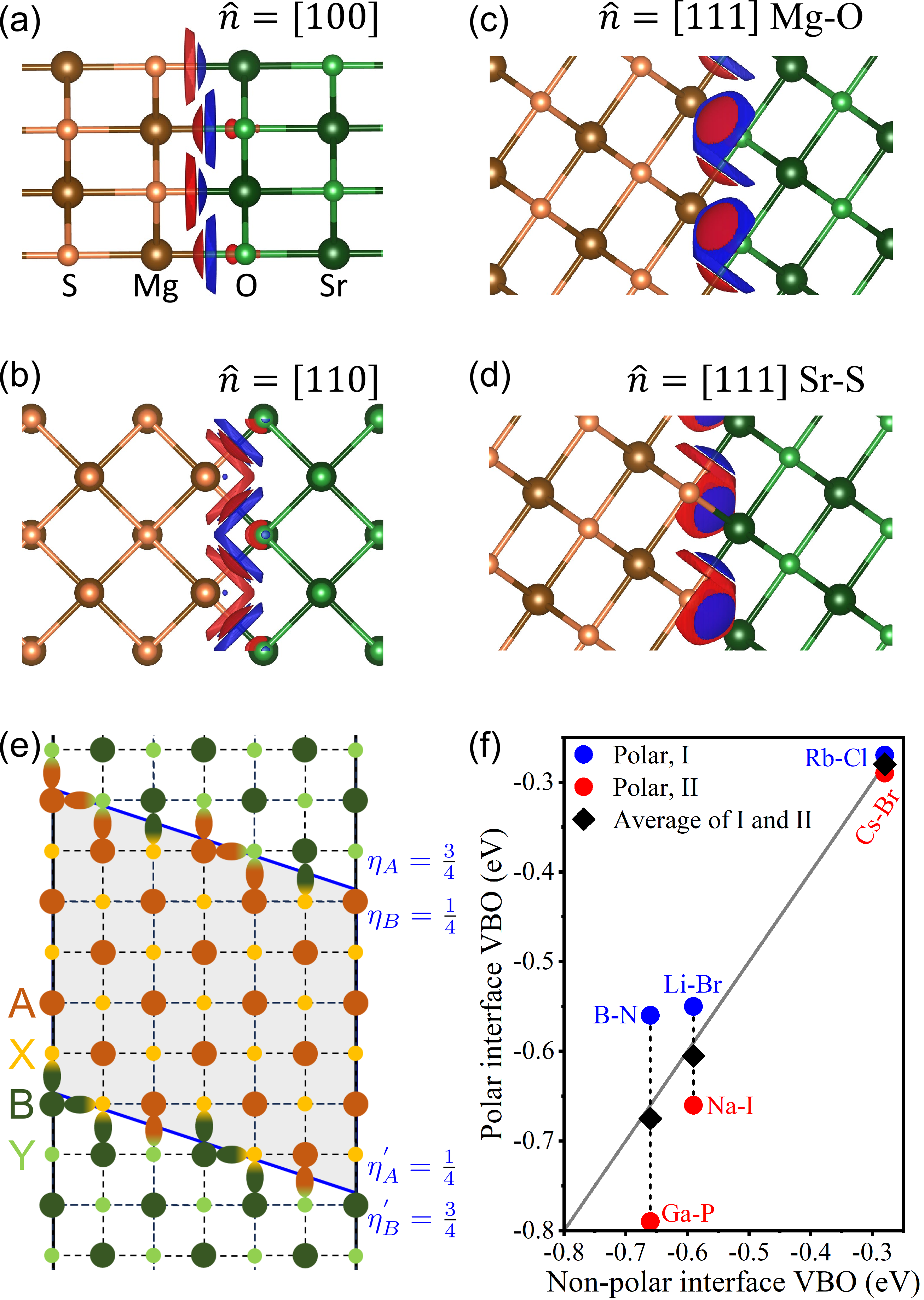
The surface of a binary can be either non-polar or polar, of which the essential difference is that non-polar surface contains an equal number of cations and anions while for a polar surface their numbers are different. When reconnecting two dissimilar binaries, two types of interfacial bonds can form depending on how the surfaces are terminated. Considering two binaries AX and BY with A, B (X, Y) being the cations (anions), both A-Y and B-X bonds can form at the interface. The key point is that a non-polar interface contains two types of interfacial bonds with equal populations, while the relative proportions of the two bond types are different for polar interfaces. This is exemplified using MgS-SrO interface shown in Figs. 4(a-d), where (a-b) are non-polar interfaces with equal numbers of Mg-O and Sr-S bonds while (c) and (d) are polar interfaces containing only Mg-O or Sr-S bonds, respectively. While these are limiting cases, in general we can define () which are the relative concentrations of bond-type A (B) at the interface. As the basic geometric properties of the interface are unchanged for the case of binaries, we can then generalize Eq. (9) as
| (11) |
where and are the bond dipoles associated with the two types of interfacial bonds (i.e., associated with A-Y and B-X bonds, respectively). Here we note that the concentrations and depend not only on orientation, but also on the position of the interfacial plane which leads to different types of polar surfaces. Nevertheless, we can see that for any non-polar interface and by taking , the orientation independence given by Eq. (10) is strictly restored.
For polar directions, however, changing the interface position is associated with the change of s and can lead to different interfacial dipoles. Taking MgS-SrO [111] as an example, two different interfaces can be constructed as illustrated in Figs. 4(c-d), where the interfacial bonds can be either Mg-O or Sr-S depending on the termination. These two polar interfaces can be described by (, ) and (, ), with interfacial dipoles of and , respectively. A more general example is shown in Fig. 4(e) with the 2D checkerboard lattice where two complementary interfaces are shown by blue solid lines. Two different polar interfaces with opposite relative concentrations , and , are observed. Here we see that the summation of the relative concentrations of two complementary polar interfaces equals to twice of the value of a non-polar interface. Thus, the interfacial dipole associated with the non-polar interface is the average of the two complimentary polar interfaces,
| (12) |
Thus, the orientation independence of band offset in polar directions can be understood from their average effect. This relation is also demonstrated from direct calculation in Fig. 4(f), where are shown in blue(red) and their average value (black) is found to be quite close to the non-polar interfacial dipole indicated by the line.
We can see that the band offset of a single polar interface is different from that of non-polar directions and depends on the atomic termination of interface plane. As an example[43], it is experimentally seen that the VBO of GaAs-ZnSe [100] interface can be tuned from 0.6 to 1.1 eV by controlling the atomic configuration of interface. However, more experimental interests are usually given to a special case that two constituent materials of the interface have a common anion/cation, e.g., AlAs-GaAs[13] and CdTe-HgTe[14], where the band offset is found to be consistent between polar and non-polar interface. In such cases, two complementary polar interfaces becomes equivalent under a lattice translation along the interface normal direction. This symmetry forces two types of bond dipoles and , which although are associated to different interfacial bonds, to have the same magnitude . Thus, is single-valued for a common-anion/cation interface even in the polar directions and the orientation independence of band offset is rigorously restored for any orientation.
II.5 Band offset in anisotropic systems
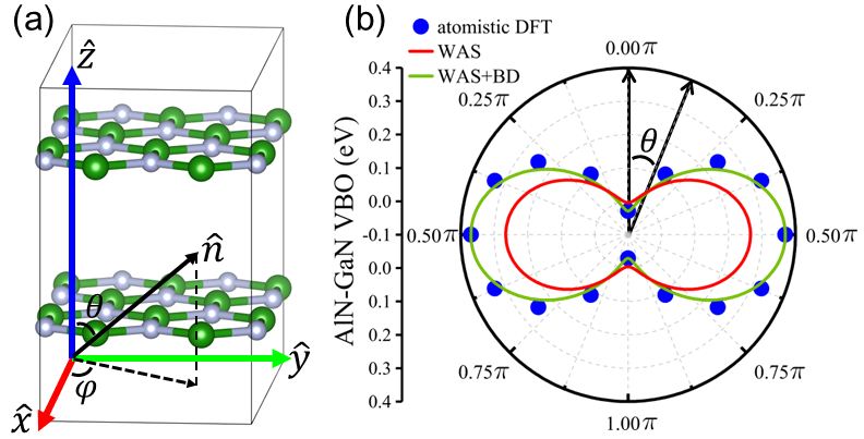
The orientation independent band offset of isotropic systems is a direct result of crystal symmetry, thus an investigation of band offset in highly anisotropic systems provides a chance to examine our knowledge learned from isotropic systems. Here we consider the interface between two van der Waals (vdW) materials, AlN and GaN, which are both layered hexagonal lattices with AA stacking. As shown in Fig. 5(a), any surface normal direction can be represented by two angles, and ,
| (13) |
Considering the quadrupole potential shift in Eq. (2), we can write it in terms of and as
| (14) | ||||
Here the cross terms of quadrupole in Eq. (14) vanish due to the 2D isotropy of hexagonal lattice and the mirror symmetry of AA stacking. By first taking the integral to calculate the quadrupole and then summing over all the species in Eq. (14), the potential shift is given as
| (15) | ||||
where , and are the electric quadrupole of a unit cell in , and directions. Using Eq. (1), Eq. (15) can also be rewritten as,
| (16) | ||||
The band offset of a Wigner-Seitz interface is obtained by taking the difference of Eq. (16) between two dissimilar materials across the interface. The bulk quadrupole contribution to the band offset becomes orientation dependent due to that the quadrupoles are not isotropic.
Considering the interfacial dipole relaxation, there are two types of interfacial chemical bonds in the hexagonal layer, Al-N and Ga-N bonds. Here, we focus on the VBO for non-polar interfaces (or alternately the average of two complementary polar interfaces). Similar to Eqs. (11-12), for non-polar interfaces there are an equal number of Al-N and Ga-N bond dipoles and hence they can be grouped into an effective dipole in the hexagonal layer. In principle, there could also be a bond dipole associated with vdW binding which we define as . For each type of bond, by inserting Eq. (13) into the general expression Eq. (9) of , we get
| (17) | ||||
where the bracketed terms are the interfacial dipole density for an interface with the normal direction in , and , respectively. By summing the contributions of and , can be expressed as
| (18) |
Similar to Eq. (14), Eqs. (17-18) rely on the 2D isotropy of hexagonal lattice and the mirror symmetry of AA stacking which guarantees the cross terms in vanish in the sum over for the strong chemical bonds and vdW binding, respectively.
Combining Eqs. (16) and (18), the VBO in any direction is
| (19) | ||||
Eq. (18) takes into account both bulk quadrupole and interfacial dipole contributions to the band offset with the only assumption that the bond dipoles are unaffected by the interfacial orientation. In Fig. 5(b) we compare the band offset results of Wigner-Seitz interface, Eq. (19) and the atomistic DFT calculations for AlN-GaN heterostructure. Since the hexagonal lattice is isotropic in 2D, the angle in the - plane does not affect the result of band offset for non-polar interfaces. Here we choose a special in our calculation.
III Conclusion
By partitioning the bulk charge density into charge neutral ion-centered Wigner-Seitz atoms which obey the bulk crystal symmetry, we provide a bulk reference for the formation of the interface. The bulk contribution to the band offset is then expressed in terms of the quadrupole moments of the constituent Wigner-Seitz atoms, which provides an orientation independent bulk contribution to the band offset for isotropic materials. Furthermore, this allows for determination of the charge transfer at the interface, which is found to be a manifestation of localized charge transfer along the interfacial bonds. By constructing a simple model of the interfacial charge transfer dipole as originating from the sum of localized bond dipoles, we show that the direction dependence of the VBO for isotropic and anisotropic systems (both polar and non-polar) can be understood in a unified framework. For isotropic systems, it provides a clear-cut explanation on the nearly orientation independent band offsets observed in experiments and calculations and for anisotropic systems, it correctly describes the orientation dependent band offset. These results suggest some deeper physics underlying the Wigner-Seitz charge partitioning and point to its wider application in the study of band offset for microelectronics.
IV Method
DFT calculations are carried out by VASP code[44] with PBE[45] functional. The lattice structure of materials are taken from Material Porject[46] database. A plane-wave cutoff of 400 eV is used. The properties of Wigner-Seitz atoms/surfaces/interfaces are determined from bulk unit cell calculations. The atomistic DFT result of valence band offset is determined from a direct supercell calculation, in which the interface supercell is constructed by connecting the bulk supercells of two constituent materials along the interface normal direction. The interfacial electron density is fully relaxed with frozen atomic positions to determine the interfacial dipoles. Here the effect of interfacial atomic relaxation is ignored since only lattice matched materials are considered. The convergence of valence band offset on supercell length is examined to ensure an error 0.01 eV.
Acknowledgments: This work was supported by the U.S. DOE Grant No. DE-SC0002623. The supercomputer time sponsored by National Energy Research Scientific Center (NERSC) under DOE Contract No. DE-AC02-05CH11231 and the Center for Computational Innovations (CCI) at Rensselaer Polytechnic Institute (RPI) are also acknowledged.
Author contributions: Z.Y.J. did the calculations. Z.Y.J., D.W., and S.B.Z. did the theoretical analyses. The paper is written by Z.Y.J. and D.W. with the help of S.B.Z.. S.B.Z. proposed and initiated the project.
Competing interests: All authors declare no financial or non-financial competing interests.
Data availability: The datasets used during the current study available from the corresponding author upon reasonable request.
References
- [1] Ohno, Y., Young, D. K., Beschoten, B., Matsukura, F., Ohno, H., & Awschalom, D. D., Electrical spin injection in a ferromagnetic semiconductor heterostructure, Nature 402, 790 (1999).
- [2] Chakhalian, J., Millis, A. J., & Rondinelli, J., Whither the oxide interface, Nat. Mater. 11, 92 (2012).
- [3] Hwang, H. Y., Iwasa, Y., Kawasaki, M., Keimer, B., Nagaosa, N., & Tokura, Y., Emergent phenomena at oxide interfaces, Nat. Mater. 11, 103 (2012).
- [4] Alferov, Z. I., Nobel Lecture: The double heterostructure concept and its applications in physics, electronics, and technology, Semiconductors 32, 1 (1998).
- [5] Wang, H. L., Zhang, L. S., Chen, Z. G., Hu, J. Q., Li, S. J., Wang, Z. H., Liu, J. S., & Wang, X. C., Semiconductor heterojunction photocatalysts: design, construction, and photocatalytic performances, Chem. Soc. Rev. 43, 5234 (2014).
- [6] Kamat, P. V., Manipulation of charge transfer across semiconductor interface. A criterion that cannot be ignored in photocatalyst design, J. Phys. Chem. Lett. 3(5), 663 (2012).
- [7] Chuang, C. M., Brown, P. R., Bulović, V., & Bawendi, M. G., Improved performance and stability in quantum dot solar cells through band alignment engineering, Nature Mater. 13, 796 (2014).
- [8] Shao, S., & Loi, M. A., The role of the interfaces in perovskite solar cells, Adv. Mater. Interfaces 7, 1901469 (2020).
- [9] Li, Y., Zhang, J. W., Chen, Q. G., Xia, X. H., & Chen, M. H., Emerging of heterostructure materials in energy storage: a review, Adv. Mater. 33, 2100855 (2021).
- [10] Sun, X., Zhu, C., Zhu, X., Yi, J., Liu, Y., Li, D., & Pan, A., Recent advances in two‐dimensional heterostructures: From band alignment engineering to advanced optoelectronic applications, Adv. Electron. Mater. 7, 2001174 (2021).
- [11] Wang, W. I., Kuan, T. S., Mendez, E. E., & Esaki, L., Evidence of orientation independence of band offset in AlGaAs/GaAs heterostructures, Phys. Rev. B 31, 6890(R) (1985).
- [12] Langer, J. M., & Heinrich, H., Deep-level impurities: A possible guide to prediction of band-edge discontinuities in semiconductor heterojunctions, Phys. Rev. Lett. 55, 1414 (1985).
- [13] Hirakawa, K., Hashimoto, Y., & Ikoma, T., Orientation independence of heterojunction‐band offsets at GaAs‐AlAs heterointerfaces characterized by x‐ray photoemission spectroscopy, Appl. Phys. Lett. 57, 2555–2557 (1990).
- [14] Becker, C. R., Wu, Y. S., Waag, A., Kraus, M. M., & Landwehr, G., The orientation independence of the CdTe-HgTe valence band offset as determined by X-ray photoelectron spectroscopy, Semicond. Sci. Technol. 6, C76-C79 (1991).
- [15] Yu, E. T., McCaldin, J. O., & McGill, T. C., Band offsets in semiconductor heterojunctions, Solid State Phys. 46, 1 (1992).
- [16] Van de Walle, C. G., & Martin, R. M., Theoretical study of band offsets at semiconductor interfaces, Phys. Rev. B 35, 8154 (1987).
- [17] Baldereschi, A., Baroni, S., & Resta, R., Band offsets in lattice-matched heterojunctions: a model and first-principles calculations for GaAs/AlAs, Phys. Rev. Lett. 61, 734 (1988).
- [18] Christensen, N. E., Dipole effects and band offsets at semiconductor interfaces, Phys. Rev. B 37, 4528 (1988).
- [19] Christensen, N. E., Possibility of heterostructure band offsets as bulk properties: Transitivity rule and orientation effects, Phys. Rev. B 38, 12687 (1988).
- [20] Wei, S. H., & Zunger, A., Calculated natural band offsets of all II–VI and III–V semiconductors: Chemical trends and the role of cation d orbitals, Appl. Phys. Lett. 72, 2011 (1998).
- [21] Li, Y. H., Walsh, A., Chen, S. Y., Yin, W. J., Yang, J. H., Li, J. B., Da Silva, J. L. F., Gong, X. G., & Wei, S. H., Revised ab initio natural band offsets of all group IV, II-VI, and III-V semiconductors, Appl. Phys. Lett. 94, 212109 (2009).
- [22] Zhang, S. B., Cohen, M. L., Louie, S. G., Tomanek, D., & Hybertsen, M. S., Quasiparticle band offset at the (001) interface and band gaps in ultrathin superlattices of GaAs-AlAs heterojunctions, Phys. Rev. B 41, 10058 (1990).
- [23] Xucun, M., Jiang, P., Qi, Y., Jia, J., Yand, Y., Duan, W., Li, W. X., Bao, X., Zhang, S. B., & Xue, Q-K., Experimental observation of quantum oscillation of surface chemical reactivities, PNAS 104, 9204 (2007).
- [24] Anderson, R. L., Germanium-gallium arsenide heterojunctions, IBM J. Res. Develop. 4, 283 (1960).
- [25] Besse, R., Silveira, J. F. R. V., Jiang, Z. Y., West, D., Zhang, S. B., & Da Silva, J. L. F., Beyond the Anderson rule: importance of interfacial dipole and hybridization in van der Waals heterostructures, 2D Mater. 8, 041002 (2021).
- [26] Cardona, M., & Christensen, N. E., Acoustic deformation potentials and heterostructure band offsets in semiconductors, Phys. Rev. B 35, 6182 (1987).
- [27] Jaros, M., Simple analytic model for heterojunction band offsets, Phys. Rev. B 37, 7112 (1988).
- [28] Lambrecht, W. R. L., & Segall, B., Interface dependence of band offsets in lattice-matched isovalent heterojunctions, Phys. Rev. B 41, 8353 (1990).
- [29] Tersoff, J., Schottky barrier heights and the continuum of gap states, Phys. Rev. Lett. 52, 465 (1984).
- [30] Tersoff, J., Theory of semiconductor heterojunctions: The role of quantum dipoles, Phys. Rev. B 30, 4874(R) (1984).
- [31] Tersoff, J., Schottky barriers and semiconductor band structures, Phys. Rev. B 32, 6968(R) (1985).
- [32] Schleife, A., Fuchs, F., Rödl, C., Furthmüller, J., & Bechstedt, F., Branch-point energies and band discontinuities of III-nitrides and III-/II-oxides from quasiparticle band-structure calculations, Appl. Phys. Lett. 94, 012104 (2009).
- [33] Hinuma, Y., Grüneis, A., Kresse, G., & Oba, F., Band alignment of semiconductors from density-functional theory and many-body perturbation theory, Phys. Rev. B 90, 155405 (2014).
- [34] Wigner, E., & Seitz, F., On the constitution of metallic sodium, Phys. Rev. 43, 804 (1933).
- [35] Grosso, G., & Parravicini, G. P., Solid State Physics (Academic Press, UK, 2014).
- [36] Conway, J. H., Burgiel, H., & Goodman-Strauss, C., The Symmetries of Things (AK Peters, Wellesley, MA, 2008).
- [37] Tung, R. T., The physics and chemistry of the Schottky barrier height, Appl. Phys. Rev. 1, 011304 (2014).
- [38] Tung, R. T., & Kronik, L., Band offset formation at semiconductor heterojunctions through density-based minimization of interface energy, Phys. Rev. B 94, 075310 (2016).
- [39] Tung, R. T., & Kronik, L., Charge density and band offsets at heterovalent semiconductor interfaces, Adv. Theo. Simul. 1, 1700001 (2018).
- [40] Choe, D.-H., West, D., & Zhang, S., Band alignment and the built-in potential of solids, Phys. Rev. Lett. 121, 196802 (2018).
- [41] Choe, D-H., West, D., & Zhang, S., Revealing the vacuum level in an infinite solid by real-space potential unfolding, Phys. Rev. B 103, 235202 (2021).
- [42] Jiang, Z. Y., West, D., & Zhang, S. B., Simple and accurate estimation of metal, semiconductor, and insulator work functions, Phys. Rev. Materials 7, 015001 (2023).
- [43] Funato, M., Aoki, S., Fujita, S., & Fujita, S., Tunable band offsets via control of interface atomic configuration in GaAs-on-ZnSe (001) heterovalent heterostructures, J. Appl. Phys. 85, 1514–1519 (1999).
- [44] Kresse, G., & Furthmüller, J., Efficient iterative schemes for ab initio total-energy calculations using a plane-wave basis set, Phys. Rev. B 54, 11169 (1996).
- [45] Perdew, J. P., Burke, K., & Ernzerhof, M., Generalized gradient approximation made simple, Phys. Rev. Lett. 77, 3865 (1996).
- [46] Jain, A., Ong, S. P., Hautier, G., Chen, W., Richards, W. D., Dacek, S., Cholia, S., Gunter, D., Skinner, D., Ceder, G., & Persson, K. A., Commentary: The Materials Project: A materials genome approach to accelerating materials innovation, APL Mater. 1, 011002 (2013).