Quasiparticle band structure and excitonic optical response in V2O5 bulk and monolayer
Abstract
The electronic band structure of V2O5 is calculated using an all-electron quasiparticle self-consistent (QS) method, including electron-hole ladder diagrams in the screening of , named QS and using a full-potential linearized muffin-tin-orbital basis set. The optical dielectric function calculated with the Bethe-Salpeter equation (BSE) exhibits excitons with large binding energy, consistent with spectroscopic ellipsometry data and other recent calculations using a pseudopotential plane wave based implementation of the many-body-perturbation theory approaches. Convergence issues are discussed. Sharp peaks in the direction perpendicular to the layers at high energy are found to be an artifact of the truncation of the numbers of bands included in the BSE calculation of the macroscopic dielectric function. The static (electronic screening only) dielectric constant gives indices of refraction in good agreement with experiment. The exciton wave functions are analyzed in various ways. They correspond to charge transfer excitons with the hole primarily on oxygen and electrons on vanadium, but depending on which exciton, the distribution over different oxygens changes. The dark exciton at 2.6 eV is the most localized and has the highest weight on the bridge oxygen, while the lowest bright excitons for in-plane polarizations at 3.1 eV for and 3.2 eV for have their higher weight on the chain and vanadyl oxygens. The exciton wave functions have a spread of about 5-15Å, with asymmetric character for the electron distribution around the hole depending on which oxygen the hole is fixed at. The same method applied first to bulk layered V2O5 is here applied to monolayer V2O5. The monolayer quasiparticle gap increases inversely proportional to interlayer distance once the initial interlayer covalent couplings are removed which is thanks to the long-range nature of the self-energy and the reduced screening in a 2D system. The optical gap on the other hand is relatively independent of interlayer spacing because of the compensation between the self-energy gap shift and the exciton binding energy, both of which are proportional to the screened Coulomb interaction . Recent experimental results on very thin layer V2O5 obtained by chemical exfoliation provide experimental support for an increase in gap.
I Introduction
Exciton binding energies in some layered transition metal oxides were recently found to be extremely high, exceeding 1.0 eV.[1, 2] This is related to the relatively low dispersion band edges in these materials and the low screening of the Coulomb interaction in ionic materials, which suggest a Frenkel type exciton. V2O5 is one such layered material for which it was recently found that the excitons not only have strong binding energy but for which these excitons nonetheless exhibit not so strongly localized spatial extent and with an anisotropic delocalization in unexpected directions.[2]
The band gap in V2O5 has presented a puzzle for several years, since the first calculations were performed. While local density approximation (LDA) calculations[3] gave results close to the experimentally accepted gap of about 2.3 eV, which was extracted from Tauc plots of the optical absorption,[4] QS calculations gave a much larger band gap exceeding 4 eV.[5] These results were also confirmed by other implementations.[6, 7] This puzzle was recently resolved by showing that including electron-hole effects in the dielectric function using the Bethe-Salpeter-Equation (BSE) approach [2] gives good agreement with spectroscopic ellipsometry and reflectivity data.[8, 9] These data show indeed sharp excitonic peaks with the lowest one at about 3.1 eV for . The lower gap extracted from optical absorption is still not completely understood and may either result from excitons related to the indirect gap or phonon-mediated activation of a dark exciton.[10]
While most and BSE implementations are based on pseudopotential plane-wave basis set implementations, all-electron implementations of many-body-perturbation theory have recently become possible with linearized muffin-tin-orbital and linearized augmented plane wave basis sets.[11, 12, 13, 14, 15, 16, 17] The BSE approach was recently implemented using this approach by Cunningham et al. [18, 19]. An all-electron implementation is, in principle, preferable since it avoids the uncertainties related to choosing pseudopotentials and describes the core-valence exchange more accurately. Our first goal with the present paper is to check whether similar strong excitons are obtained with an all-electron BSE implementation and to further check the consistency of the QS band gap between all-electron and pseudopotential based implementations. Furthermore, in the usual QS approach and also in approaches, is calculated in the random phase approximation (RPA), meaning that the polarization propagator is calculated as in terms of the Green’s function and is thus represented by a simple bubble diagram. (Here is short hand for including position, spin and time variable.) The screening is thereby underestimated because it does not include electron-hole interaction effects. This has been recognized for some time as a deficiency and has been corrected among other via an excursion into time-dependent density functional theory, including a suitable exchange correlation kernel in the calculation of the polarization propagator. Shishkin et al. [20] used a kernel derived from BSE calculations, while Chen and Pasquarello[21] used the bootstrap kernel. Recently Cunningham et al. [19] proposed an alternative method to include the ladder diagrams via a BSE formulation in terms of the four-point polarization propagator. It can be viewed also as a vertex correction in the spirit of the Hedin equations.[22, 23]. Unlike the approach of Kutepov [15, 16] who implemented similar vertex corrections both in the screened Coulomb interaction with and the self-energy , and works directly toward implementing the Hedin equations self-consistently, the approach of Cunningham uses the QS approach, in which, in each iteration, the full is replaced by corresponding to an updated Hermitian non-interacting Hamiltonian . The idea is to make the dynamic perturbation from as small as possible by incorporating a static approximation of the self-energy into the exchange correlation potential of . The two Green’s functions differ by with a quasiparticle renormalization factor and the incoherent part. But in , is then largely canceled by the vertex being approximately proportional to , . This suggests that the vertex in should play a less important role in the QS approach.[11] In practice, it gives accurate quasiparticle gaps and optical spectra when BSE is used for the latter without vertex corrections in the self-energy.[19, 1] However, it has thus far been applied only to a limited number of materials. It is thus of interest to test how it works for a challenging case like V2O5.
Finally, the question arises for such layered materials, whether the band gap and optical properties will significantly change when going to the monolayer limit. From Bhandari et al. [5] it is clear that in the LDA only a small increase in gap occurs related to the breaking of some interlayer interactions and hence reduced dispersion of the valence band edge. However, in 2D materials, one expects a strong reduction of the screening when the monolayer is isolated.[24, 25] In Bhandari et al. [5] the QS gap was shown to vary as , with the interlayer distance, and this led to an extremely large gap but which was of course overestimated. Thus it becomes of great interest to study how the inclusion of electron-hole interactions in the form of ladder diagrams will affect the quasiparticle gap in a monolayer and how the reduced screening will affect the exciton binding energies and exciton spectrum. This is the second main goal of the present paper.
II Computational methods
The density functional theory (DFT) calculations and subsequent many-body-perturbation theory (MBPT) calculations are performed using the Questaal suite of codes as described in [12]. These use a full-potential linearized muffin-tin-orbital (FP-LMTO) basis set for the band structure calculations and an auxiliary mixed interstitial-plane-wave and muffin-tin partial wave product basis set for the representation of two point quantities (bare Coulomb , screened Coulomb and polarization propagator ) in the MBPT. The details of the Hedin- implementation are given in [11] and for the Bethe-Salpeter-Equation approach in Cunningham et al. [18, 19]. Briefly, in the quasiparticle-self-consistent QS method, a static and Hermitian exchange-correlation potential is extracted from the energy-dependent where the matrices are given in the basis of the Hamiltonian. The is then added to the original and defines an updated from which the next is obtained, where the energy dependent self energy is a convolution of the one-particle Green’s function and the screened Coulomb interaction. When iterated to self-consistency in , the quasiparticle energies become the same as the Kohn-Sham eigenvalues of the and the results are independent of the starting . Here we use the generalized gradient approximation (GGA) in the Perdew-Burke-Ernzerhof [26] functional as starting DFT.
The screened Coulomb interaction is normally obtained from in the random phase approximation (RPA) (i.e. using only the bubble diagram). The subscript indicates that it is calculated from the eigenstates of . Instead, in the QS method, the polarization propagator used is , which includes a summation over ladder diagrams instead of only the bubble diagram. This is done by converting to the four-particle generalized susceptibility and solving a Bethe-Salpeter Equation and then converting back to the two-particle representation,
| (1) |
with . In practice this is done expanding the four-point quantities in the basis set of single particle eigenfunctions and amounts to diagonalizing an effective two-particle Hamiltonian. It should be noted, however, that this involves solving a BSE at a mesh of -points because in we need . A static approximation is made for in Eq.(1) and the Tamm-Dancoff approximation (TDA) is made. This approach is equivalent to adding a vertex correction to in the Hedin set of equations as explained for example in [27, 28]. Details of the implementation and its justification are discussed in [19, 1].
Once the band structure is obtained in the QS or QS approximations, from which we obtain the fundamental or quasiparticle gap, we can calculate the macroscopic dielectric function for . This involves another BSE equation with the kernel
| (2) |
with the microscopic part of the bare Coulomb interaction , i.e. omitting the long-range part in a Fourier expansion. This is again done in the TDA and with a static . Here the first term in the kernel provides the local field corrections and the second provides the electron-hole interaction effects. Expanding this four-point quantity in the basis of one-particle eigenstates , one obtains an effective two-particle Hamiltonian, given by
with the Fermi occupation function for band at . Diagonalizing this Hamiltonian in the Tamm-Dancoff approximation, where is restricted to be a valence state and a conduction band state, one obtains the exciton eigenvalues and eigenvectors . Introducing the shorthand , the dielectric function is then given by
| (4) | |||||
with the matrix element
| (5) |
Here, we have assumed no spin polarization and a factor two for spin and is the number of k-points in the Brillouin zone. The limit can be taken analytically, and then involves dipole matrix elements , where gives the direction along which we take the limit to zero and which corresponds to the polarization directions of the macroscopic tensor . Finally, one converts the dipole matrix elements between Bloch states to velocity matrix elements divided by the band difference, and we then only need to diagonalize at .
Besides shifts of the oscillator strength in the continuum, it can lead to bound excitons below the quasiparticle gap. The lowest bright excitons provide the exciton gap. At present, only direct dipole matrix elements are included between the one-particle states, so we only obtain direct excitons. Lower indirect excitons which would involve a phonon assisted transition could exist but are not calculated here. The exciton eigenstates are a mixture of the vertical transition (between valence and conduction band states at a fixed k), given by
| (6) |
with , the hole and electron position of the electron-hole pair bound in the exciton. The summation over k can lead to dark excitons if at symmetry equivalent k cancel each other even if the dipole matrix elements between these states are not zero at k. The coefficients , which are the eigenvectors of the two-particle Hamiltonian can be used to ascertain, which band-pairs and at which k-points contribute to a given exciton. The exciton wavefunction modulo squared gives the probability to find the electron at position for a fixed or vice versa and is used to visualize the exciton spatial extent.
Further detail of the calculations are as follows. We use a basis set on V and O atoms, meaning that two sets of Hankel function energy and smoothing radius are used for the envelope functions of the LMTO basis set and with angular momenta up to for the first set and for the second set. Inside the spheres, the basis functions are augmented by radial functions up to and V3p semi-core orbitals are treated as local orbitals, which means they are included in the basis set rather than in the core but have only an on-site contribution and are not augmented into other spheres. We use slightly different muffin-tin spheres for the chemically different O-atoms optimized to avoid overlap between muffin-tin spheres. These are standard, well converged settings of the basis set. The self-energy matrix is calculated up to a maximum energy of 2.56 Ry and approximated by an average diagonal value above it as explained in [11].
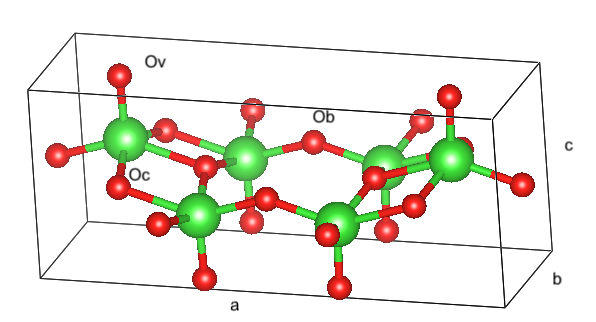
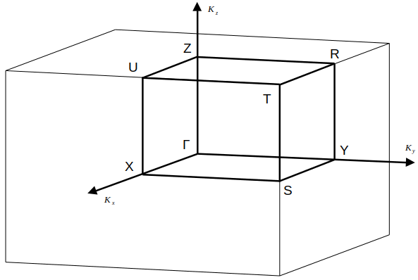
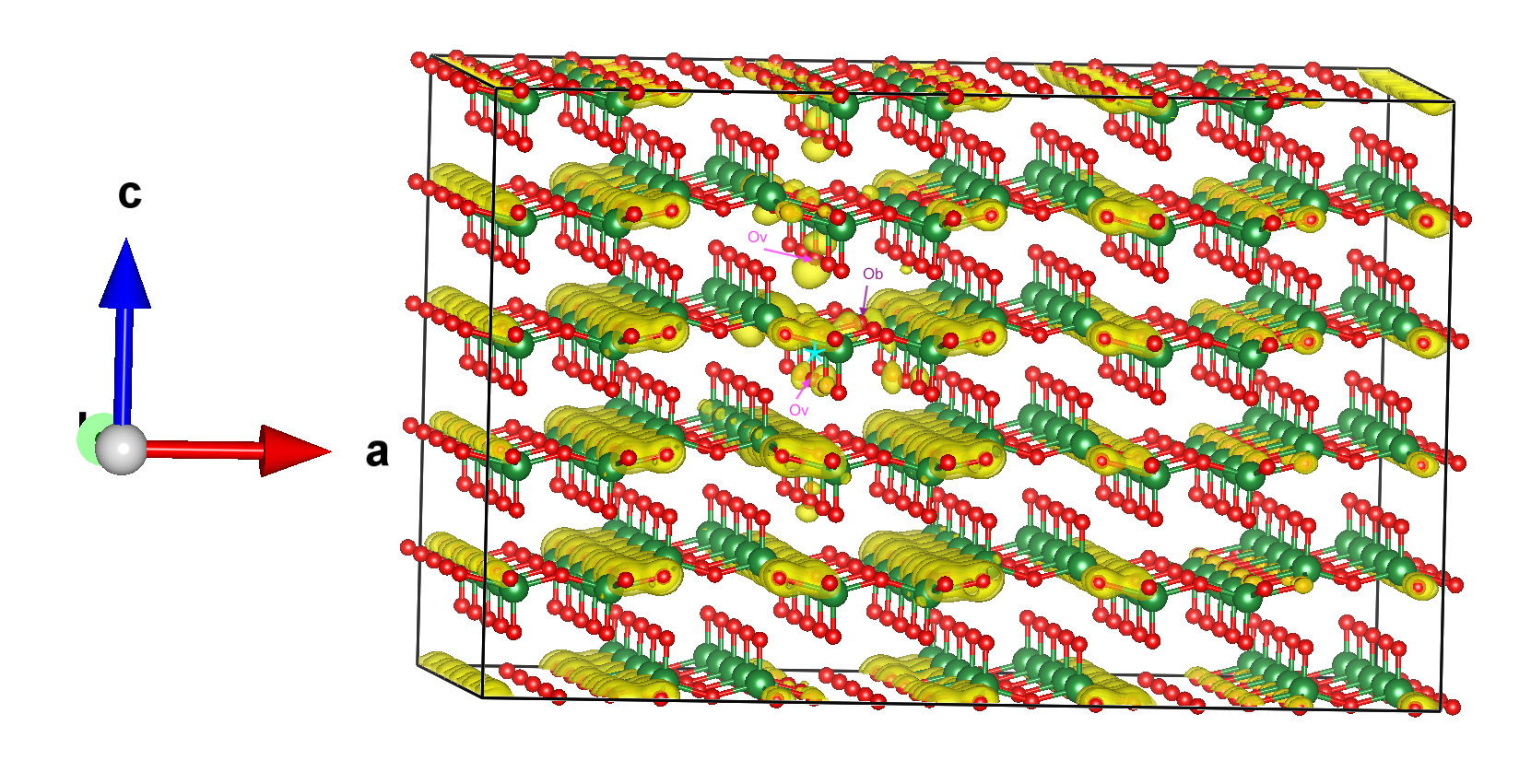
The experimental structure in the space group is used as reported by Enjalbert and Galy[29] and with lattice constants Å, Å, and Å. The structure is shown in Fig. 1 and consist of weakly van der Waals bonded layers, in the direction and double zig-zag V-O chains in the -plane along . The O in the chain are called chain oxygen, Oc and the chains are connected by bridge oxygens Ob. The vanadyl oxygens Ov are bonded to a single V and point alternating up and down along the chains but in the same direction across a bridge or rung of the ladders. This is called a ladder compound with ladders consisting of the V-Ob-V rungs. Each V is surrounded by an approximately square pyramid of 5 oxygens, one Ov, one Ob and three Oc. The corresponding Brillouin zone labeling is also shown in Fig. 1.
III Results
III.1 Bulk
III.1.1 Band structure
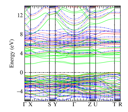
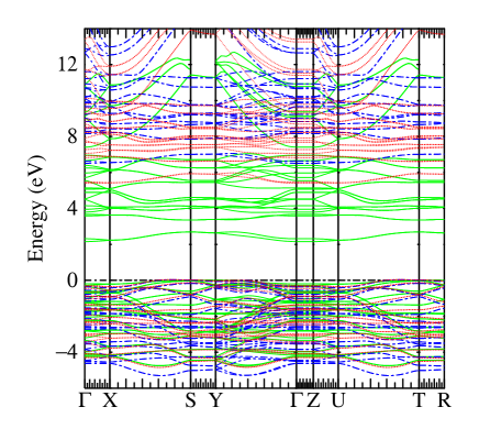
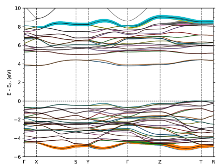
First we show the band structure obtained in , QS and QS approximations in Fig. 2. The zero is placed at the valence band maximum (VBM) of the GGA. We can thus see how the separately shifts valence bands down and conduction bands up. This assumes the charge density is not changing too much between them. We can see that the gap correction from GGA to QS occurs primarily in the conduction band. When adding the ladder diagrams, the VBM shifts back almost to the GGA position and the conduction band minimum (CBM) goes down slightly. The gaps are given in Table 1. The CBM occurs at , the VBM at T, the lowest direct gap at Z. We give the indirect gap , the lowest direct gap at and the direct gap at . We can see that the inclusion of ladder diagrams reduces the gap correction beyond GGA by a factor , close to a factor 0.8 as has been observed before for many other materials [30]. Interestingly, our all-electron QS gaps agree closely with the QS pseudopotential gaps of Gorelov et al. [2]. This indicates that some compensation of errors may affect the QS method in pseudopotential implementations, although other differences in computational detail may also affect the results.
| method | indirect | minimum direct | direct at |
|---|---|---|---|
| GGA | 1.759 | 2.041 | 2.392 |
| QS | 4.370 | 4.799 | 5.075 |
| QS | 3.781 | 4.178 | 4.452 |
| QS-pseudo 111From Gorelov et al. [2] | 3.8 | 4.4 | |
| 0.774 | 0.775 | 0.768 |
III.1.2 Imaginary part of the dielectric function
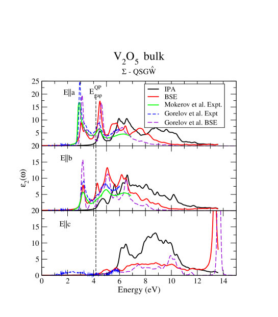
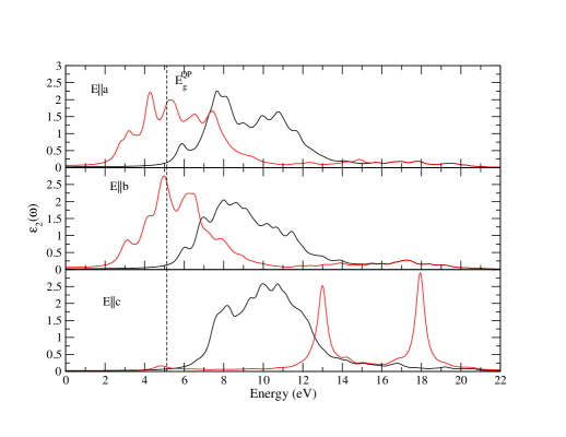
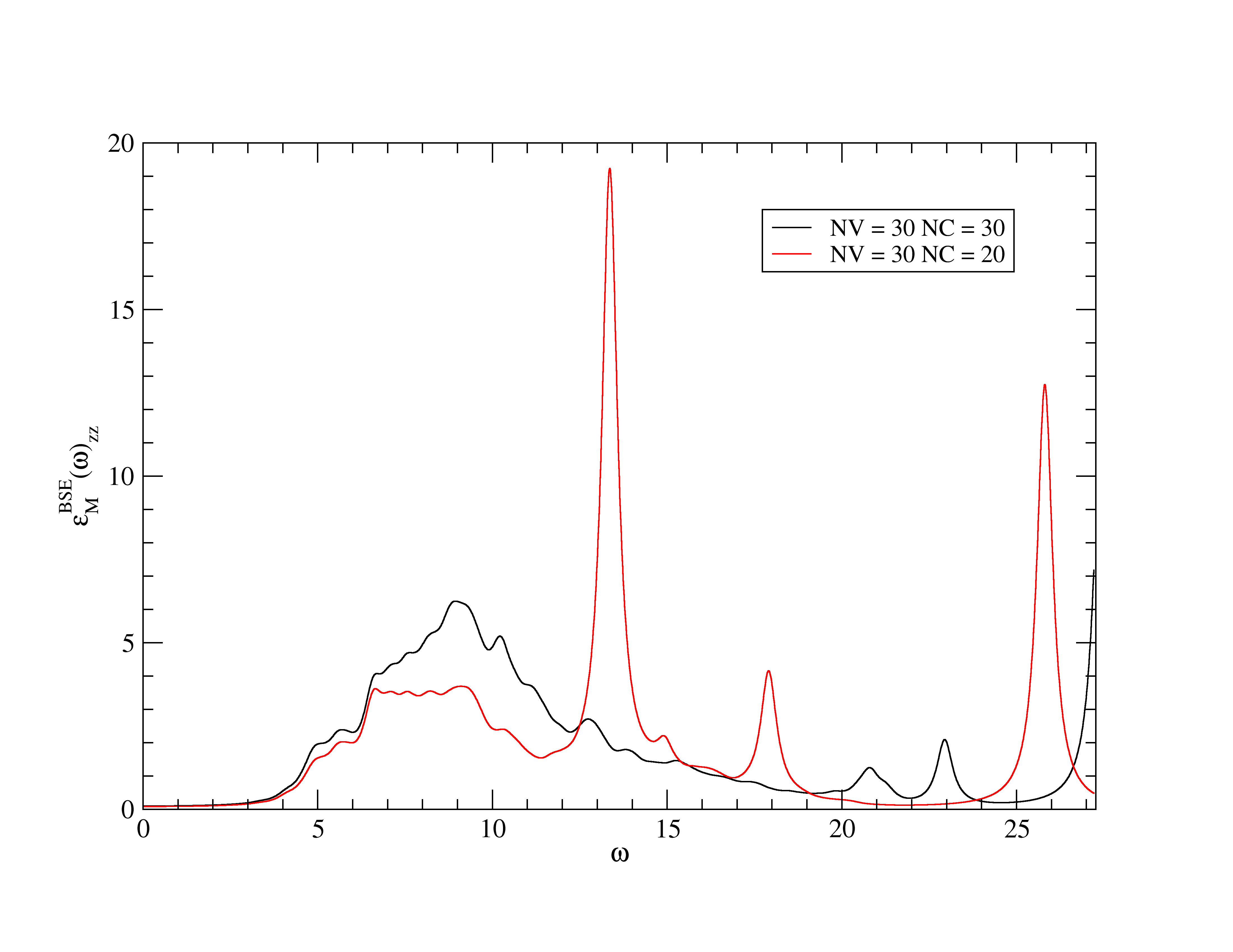
Next, in Fig. 3 we show the macroscopic dielectric function in the IPA and BSE both using the QS bands. We can see that the BSE strongly alters the dielectric function and exciton peaks with large binding energies appear significantly below the quasiparticle gap. This is in good agreement with experimental results obtained from reflectivity by Mokerov et al. [8] and more recent spectroscopic ellipsometry results as shown in Gorelov et al. [2]. We also show a comparison with the BSE results by Gorelov et al. [2]. The agreement is quite good, considering that a completely different code is used in that work and that the intensities in the exciton region were found to be quite sensitive to details of the calculation. Some of the differences with the work of Gorelov et al. [2] are that our calculation of the BSE two particle Hamiltonian includes 30 valence bands and 20 conduction bands, i.e. all O- and V- related bands, while Gorelov et al. used 15 valence bands and 16 conduction bands. We used a k-point mesh (our k-mesh calculation is identical with k-mesh calculation with only 20 meV difference in band gap) in the BSE and calculations while Gorelov et al. used a grid. We used a smaller number of k-points in the direction because the unit cell is largest in this direction and hence the Brillouin zone is smaller in this direction. For the purpose of visualizing the excitons, we subsequently used a mesh because this avoids overlapping exciton wave functions from the periodic images. However, this gives negligible differences in terms of the energy spectrum itself.
In the polarization direction perpendicular to the layers we may notice the strong suppression of BSE compared to IPA but also a sharp peak at about 13.5 eV. This was not shown in Ref. [2] because the energy scale was cut-off at lower energy but is also present in that calculation. It can also be seen in Ref. 10 although somewhat less pronounced. The suppression of the imaginary part in the BSE compared to IPA in the energy range up to 10 eV or so, is a result of strong local field effects in layered systems [31]. This is the well-known classical depolarization effect. When a dielectric layer is placed in an external field, it induces a dipole which produces a field opposite to the external field and this reduces the local field inside the layer by the dielectric constant [32].
On the other hand, the origin of the sharp peak at 13.5 eV is less clear. It is found to depend strongly on the number of bands included in the active space for the BSE calculation. When including a higher number of conduction bands, instead of , the feature disappears but sharp features still show up at even higher energy. These in turn are reduced when adding additional valence bands such as the deep lying O--bands. Further analysis discussed in Appendix A shows that it is essentially an artifact of the truncation of the active space used in the BSE calculation and the higher in energy we want accurate , the more bands we need to include.
III.1.3 Macroscopic dielectric constant from limit
In the results shown in Fig. 3 the limit of Eq. 4 is taken analytically, which requires to evaluate matrix elements of the commutator . For a local potential, these amount to well-known momentum matrix elements. However, for the QS case, the evaluation of the commutator involves the non-local self-energy operator , which requires evaluating in which the variable is Fourier transformed to reciprocal space.[33] Taking this derivative from the explicit expressions of the self-energy in terms of the LMTO basis functions is cumbersome and in the current implementation of the codes involves some additional approximations, which experience has shown to lead typically to an overestimate of the matrix elements. Alternatively, we may consider directly the dielectric function at small but finite , which is obtained as part of the procedure, and extrapolate numerically to along the three directions, , and . This can then be done both at the RPA or the BSE level. This allows us to more accurately evaluate . This amounts to the static value but including only electronic, not phonon contributions, to screening, which is conventionally called . Experimentally, this corresponds to the index of refraction squared at a frequency well below the bands but also well above the phonon frequencies, which we can compare to experimental data by Kenny and Kannewurf,[4] who obtained it by extrapolating the behavior of the index of refraction for int he region above the phonon bands. This provides an important test of the methodology because good agreement indicates that the QS method adequately describes dielectric screening.
| RPA | 1.88 | 1.83 | 1.75 |
|---|---|---|---|
| BSE | 2.37 | 2.23 | 1.92 |
| BSE | 2.44 | 2.42 | 1.99 |
| Expt.222Kenny and Kannewurf [4] | 2.07 | 2.12 | 1.97 |
Using finite small q comes with its own set of numerical difficulties. It turns out that to avoid unphysical behavior such as negative values of it is necessary to replace the bare Coulomb interaction, , by a Thomas-Fermi screened with a small . We thus need to extrapolate both and . Details of this procedure are given in Appendix B. The main results for the index of refraction are given in Table 2.
We can see that the RPA calculated dielectric constants are systematically lower than the BSE calculated ones and the RPA is clearly seen to underestimate the experimental values. The BSE results obtained with the numerical extrapolation are slightly smaller than the ones obtained with the analytically calculated matrix elements, which we call instead of . The values for and direction are close but in inverse order from the experiment and larger than for the direction but for the direction the analytically calculated value is closer to the experiment than the numerical extrapolation while the opposite is true for the in-plane directions. This illustrates the numerical difficulties with either approach. Nonetheless, overall the error in the indices of refraction is at most 15 %.
III.1.4 Exciton analysis.
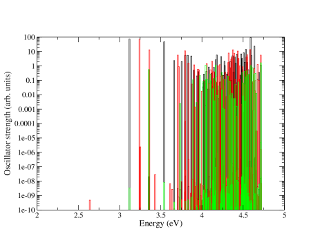
Besides the bright excitons, there are also several dark excitons. An overview of the eigenvalues of the two-particle Hamiltonian up to about the quasiparticle gap is shown in Fig. 4 as a set of bar-graphs with the oscillator strengths on a log-scale. (Note that these were obtained with and but for these low energy excitons the results are equivalent for .) Any level which has an oscillator strength lower than 0.1 may be considered dark as it is 1000 times smaller than the bright exciton oscillator strengths. These oscillator strengths are not normalized and thus given in arbitrary units. Only their relative value is important here. It is notable that an approximately doubly degenerate very dark exciton occurs well below the first bright excitons and near 2.6 eV. As was already mentioned in [2] these result from a destructive interference of the exciton eigen states at symmetry equivalent k-points rather than from zero dipole matrix elements at each individual k.
(a) 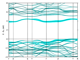 (b)
(b)  (c)
(c) 
(d) 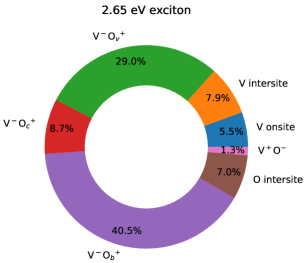 (e)
(e) 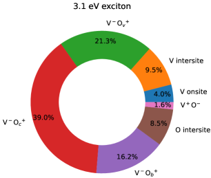 (f)
(f) 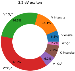
(g) 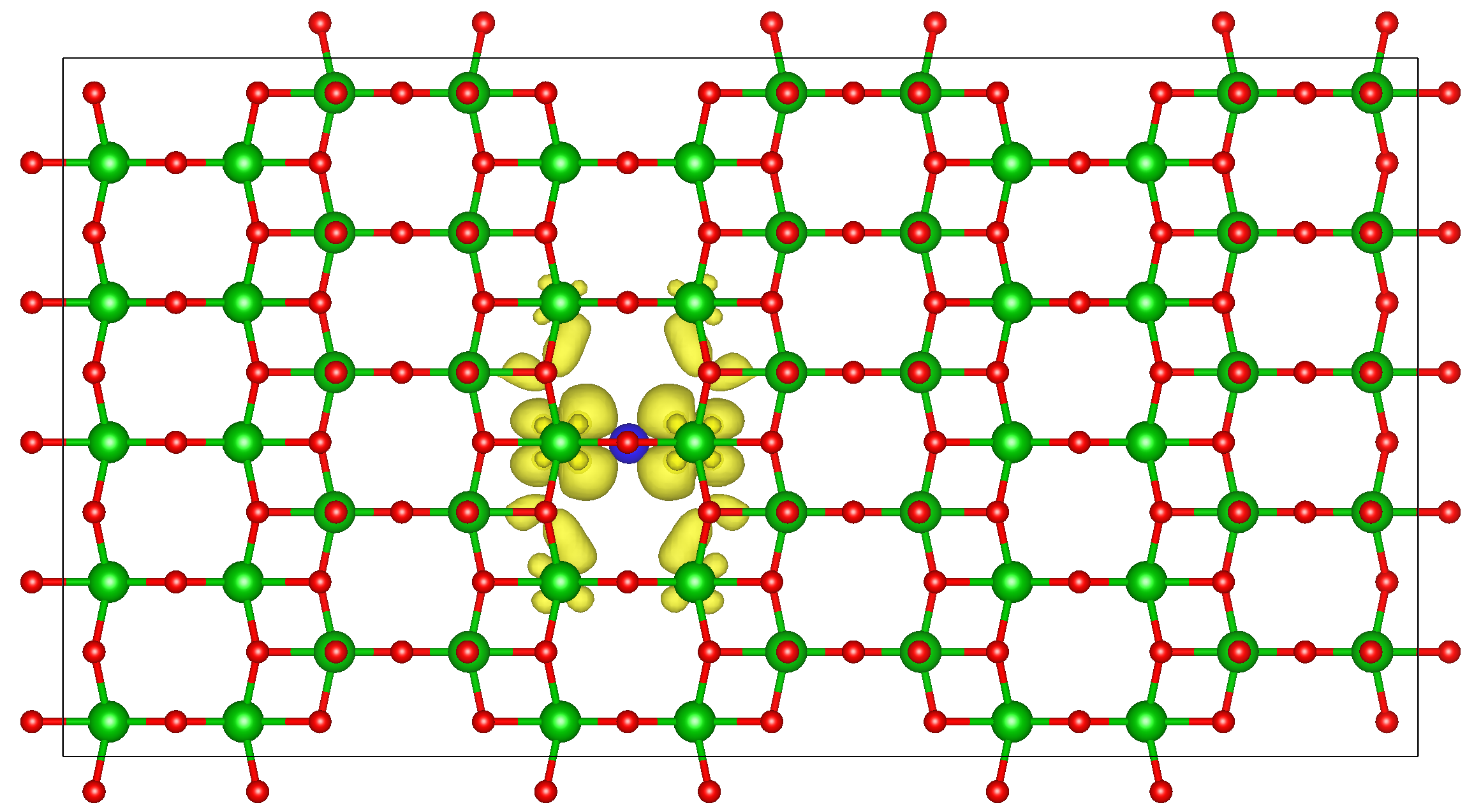 (h)
(h) 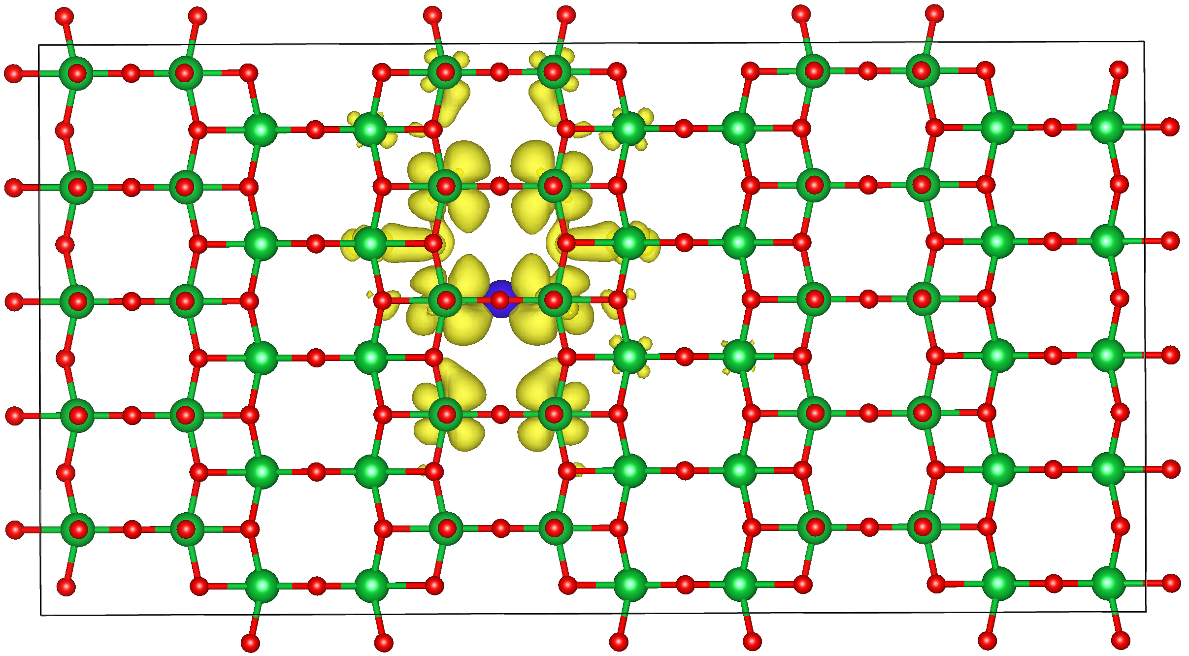 (i)
(i) 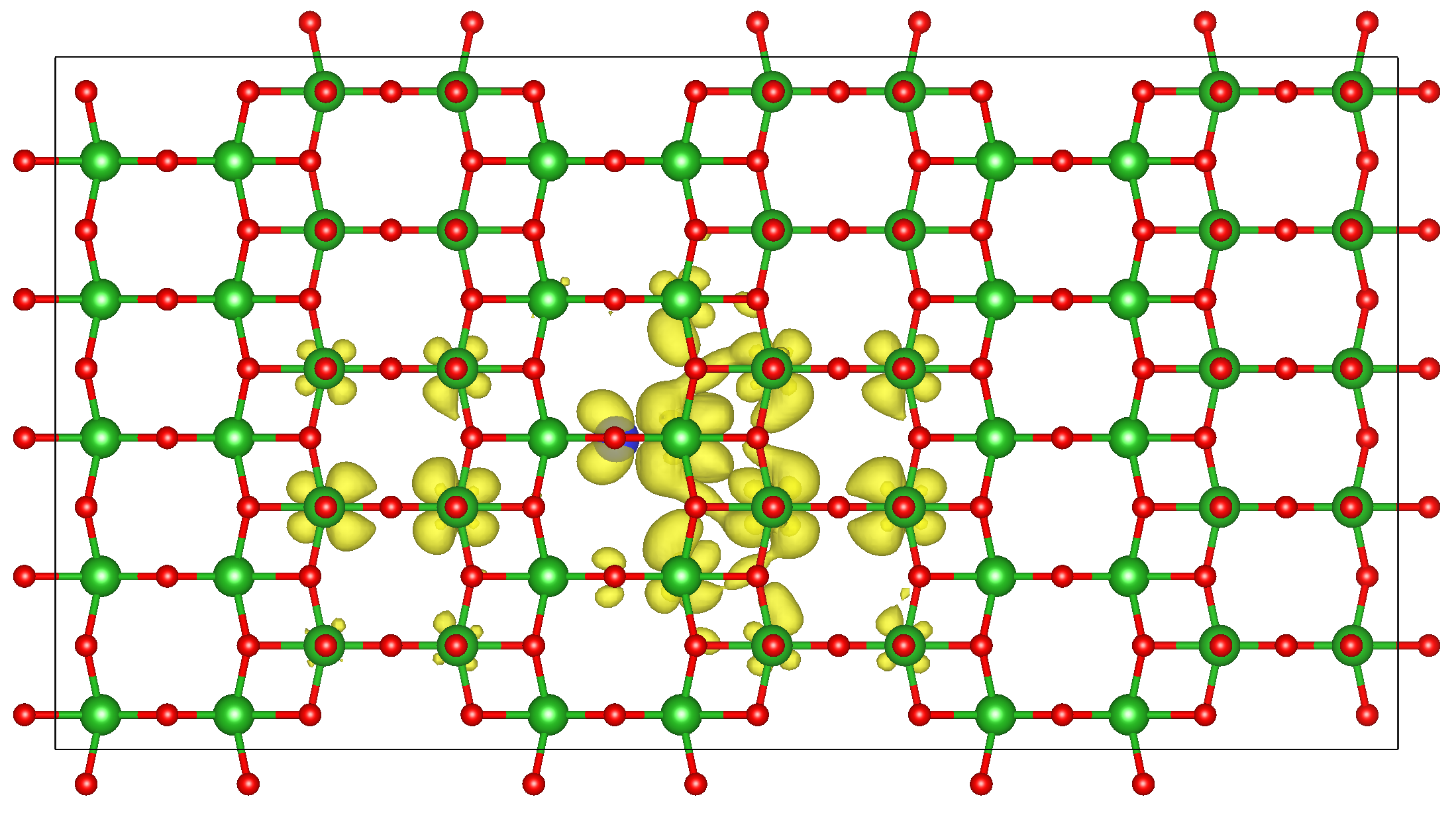
(j) 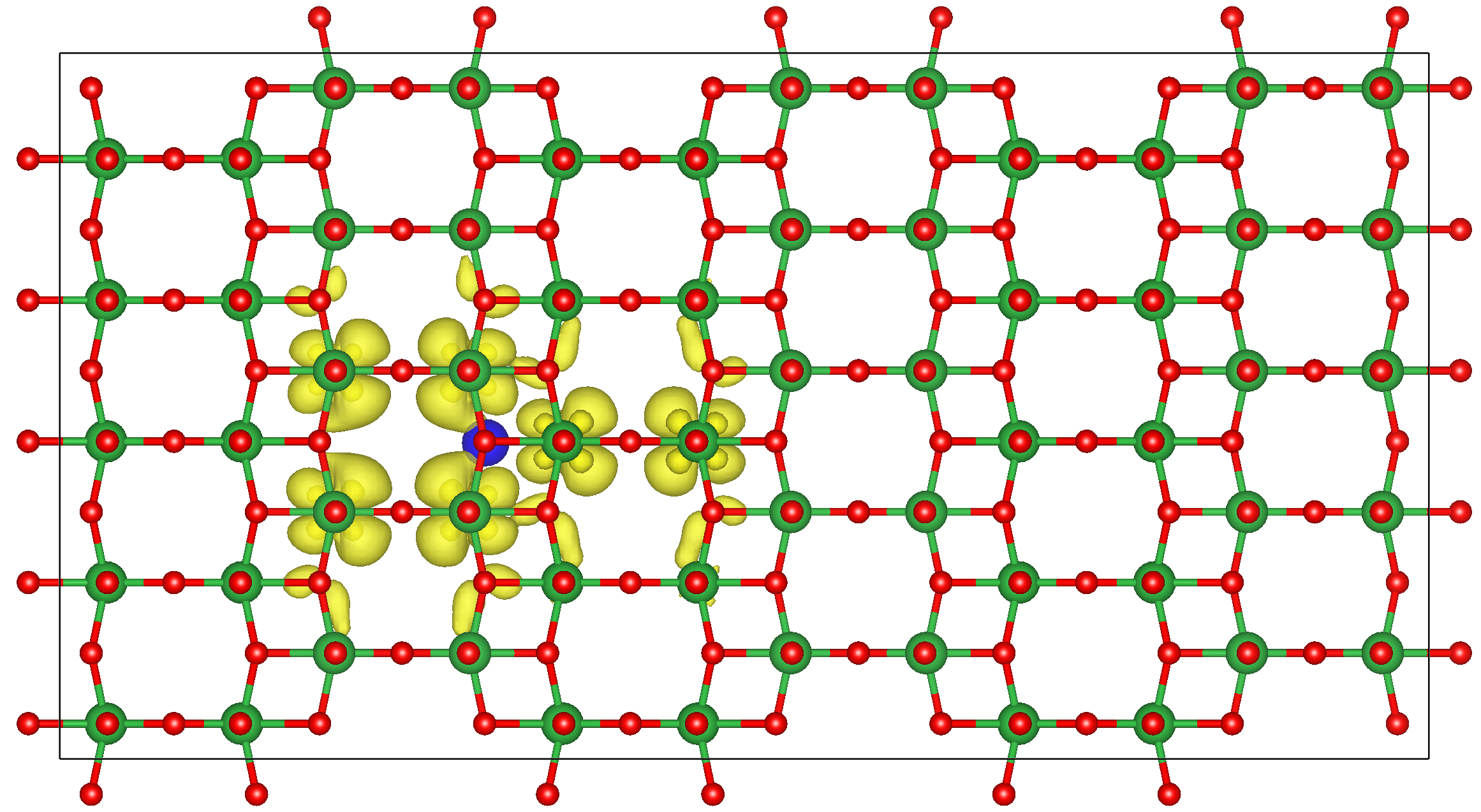 (k)
(k) 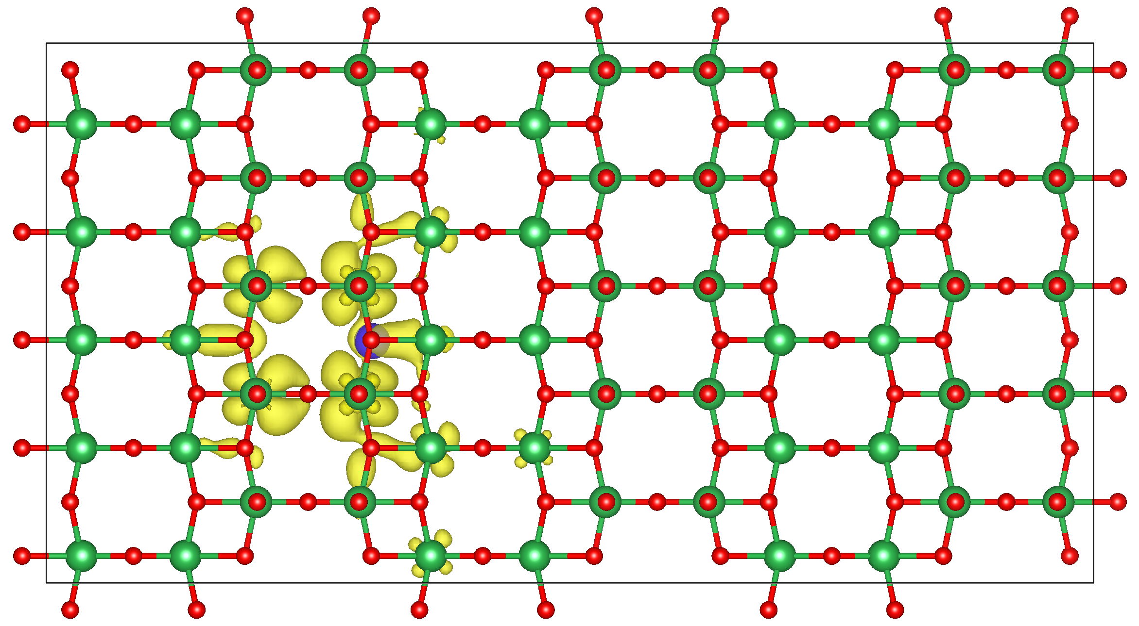 (l)
(l) 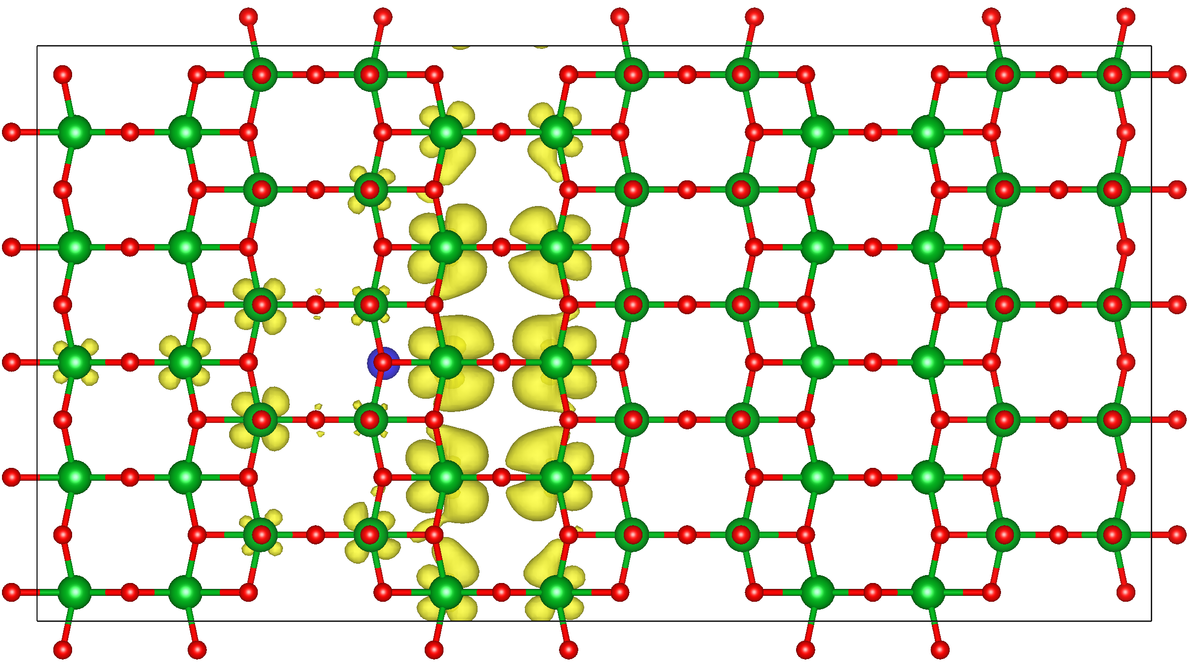
(m) 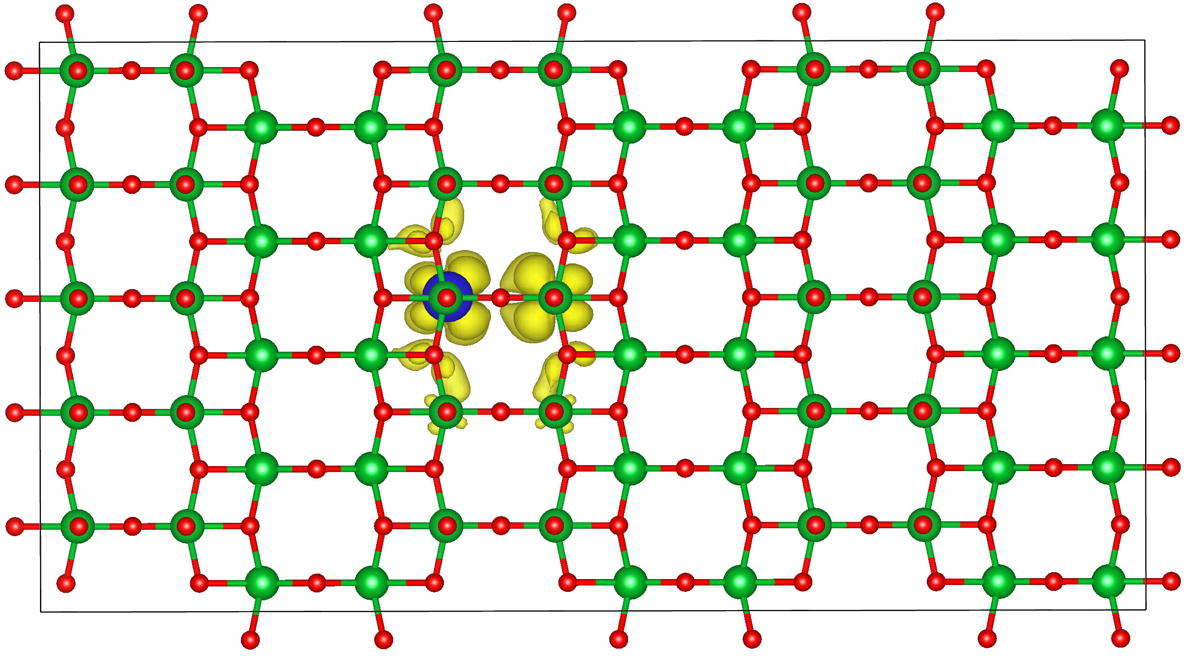 (n)
(n) 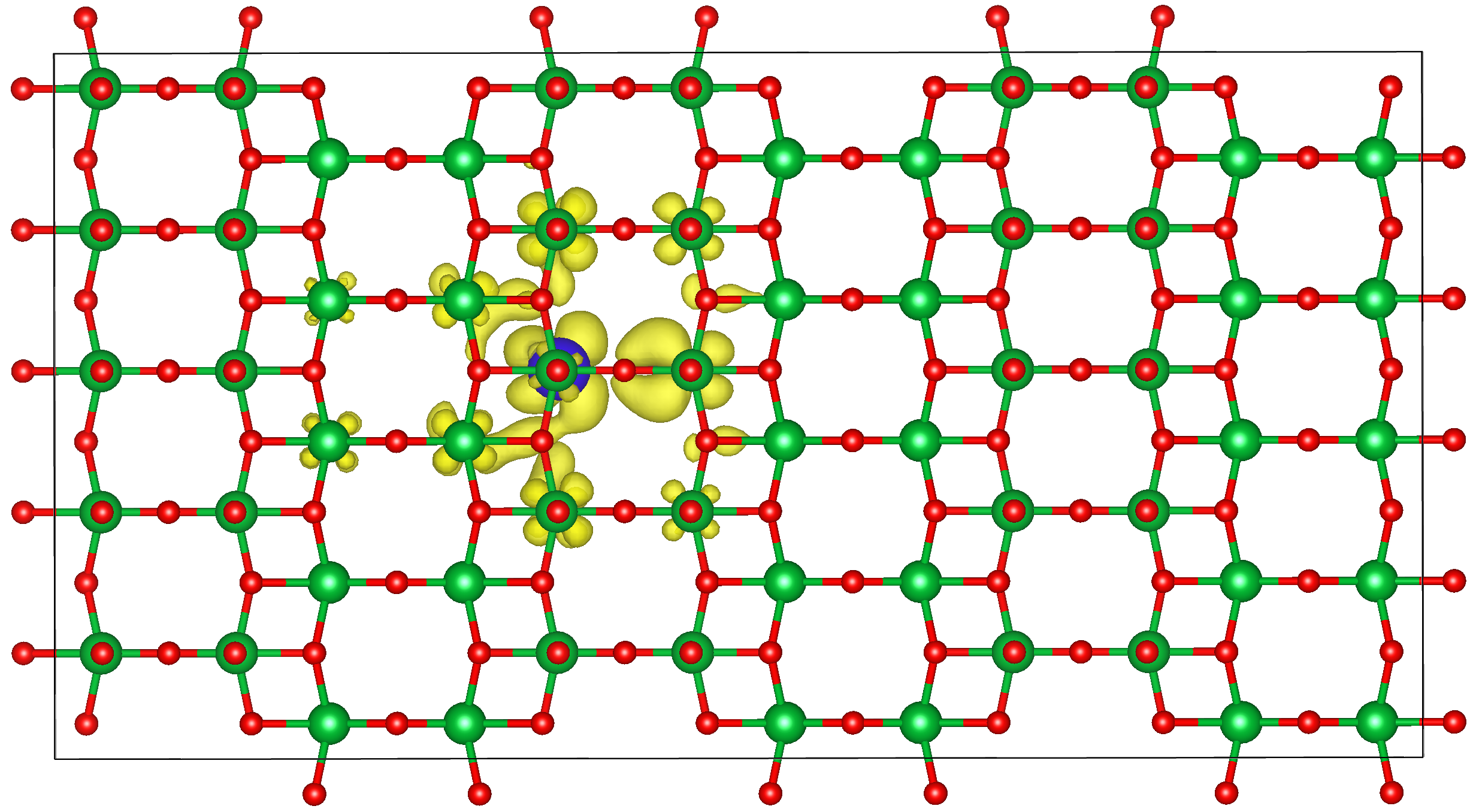 (o)
(o) 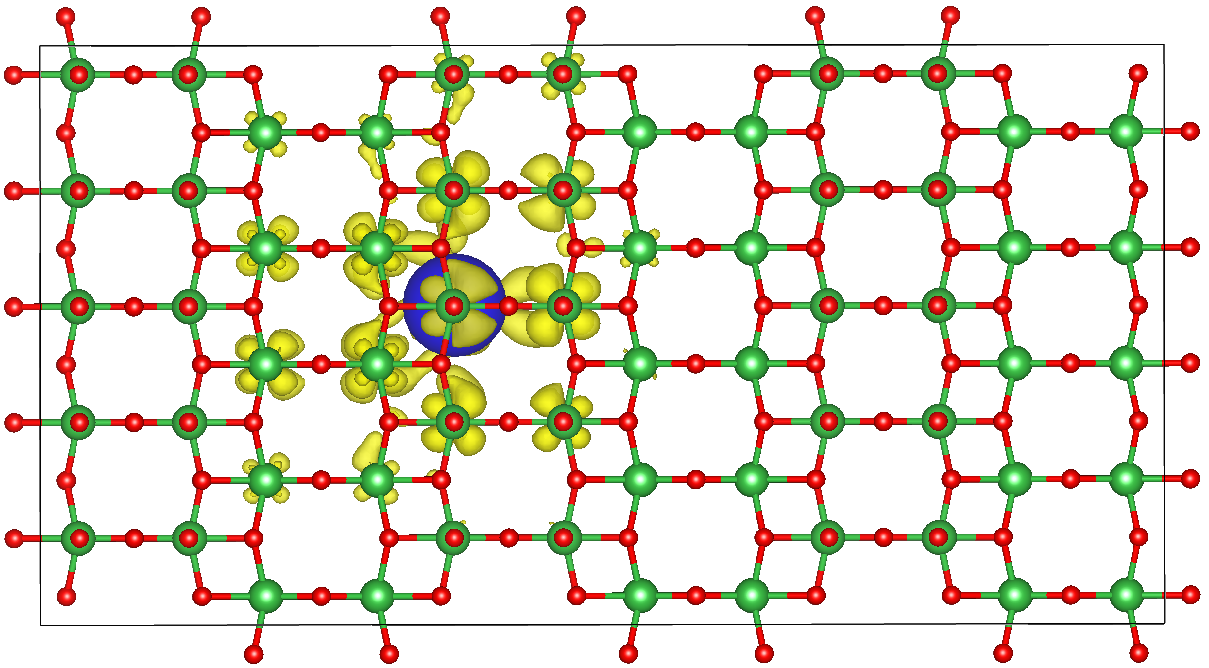
(p) 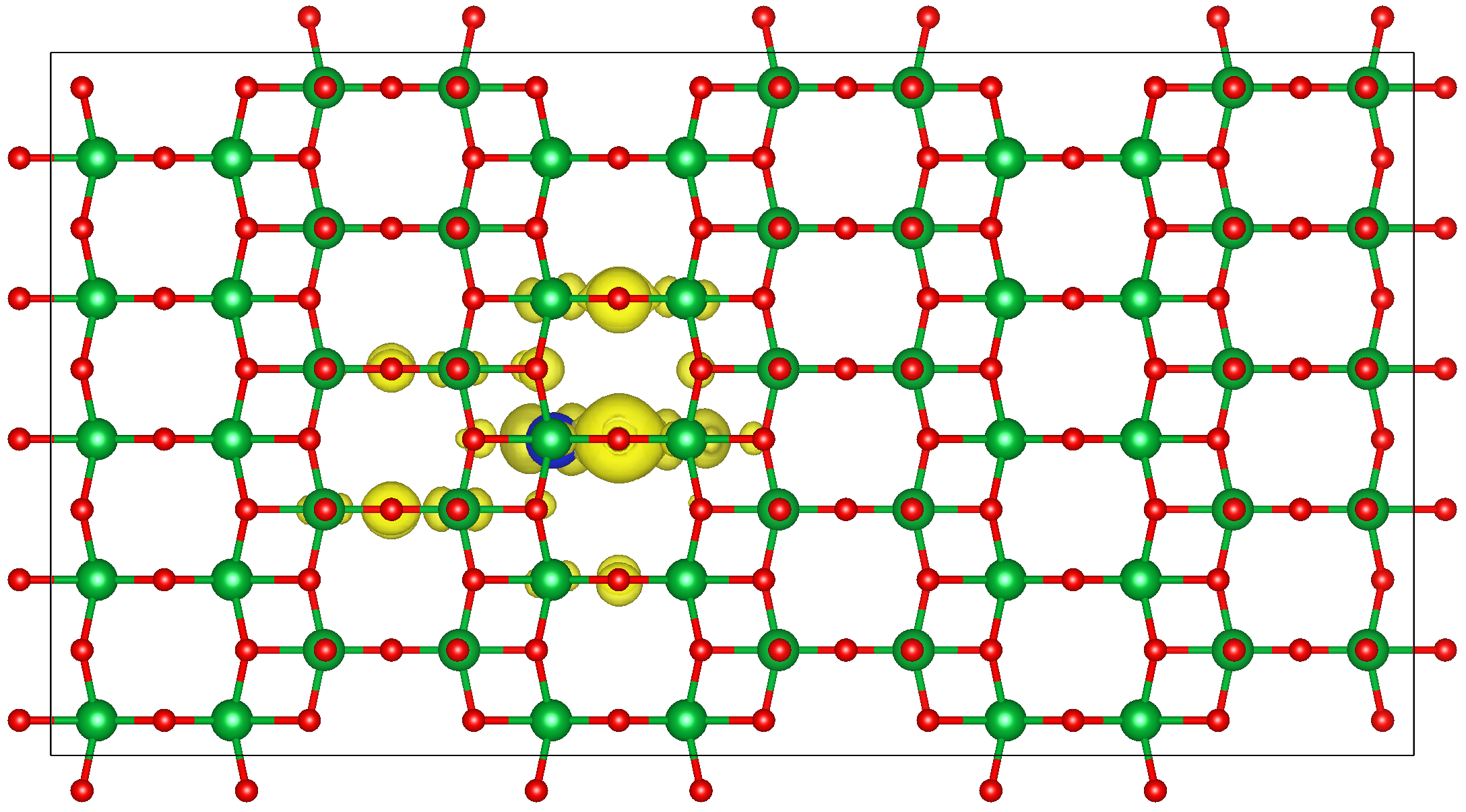 (q)
(q)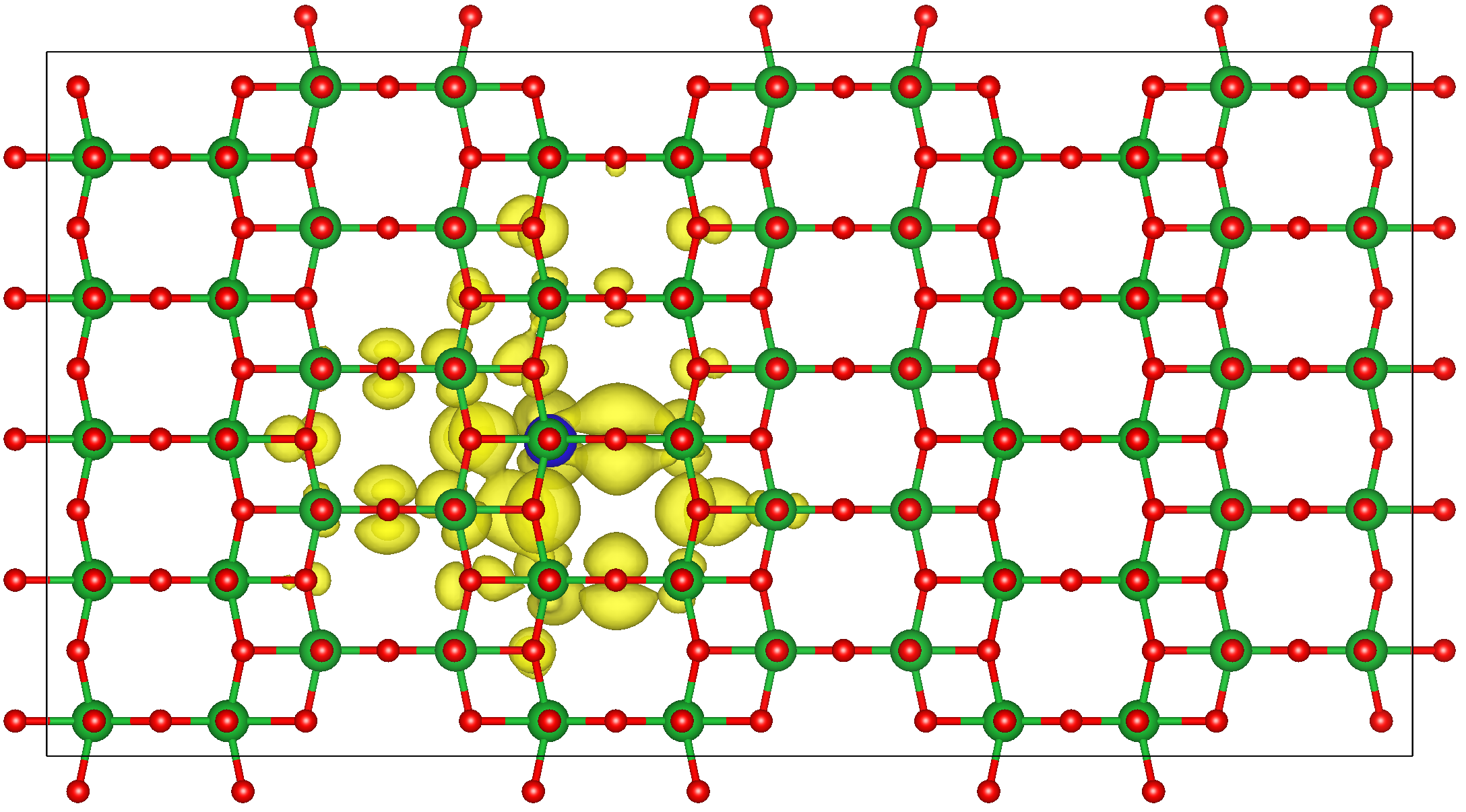 (r)
(r) 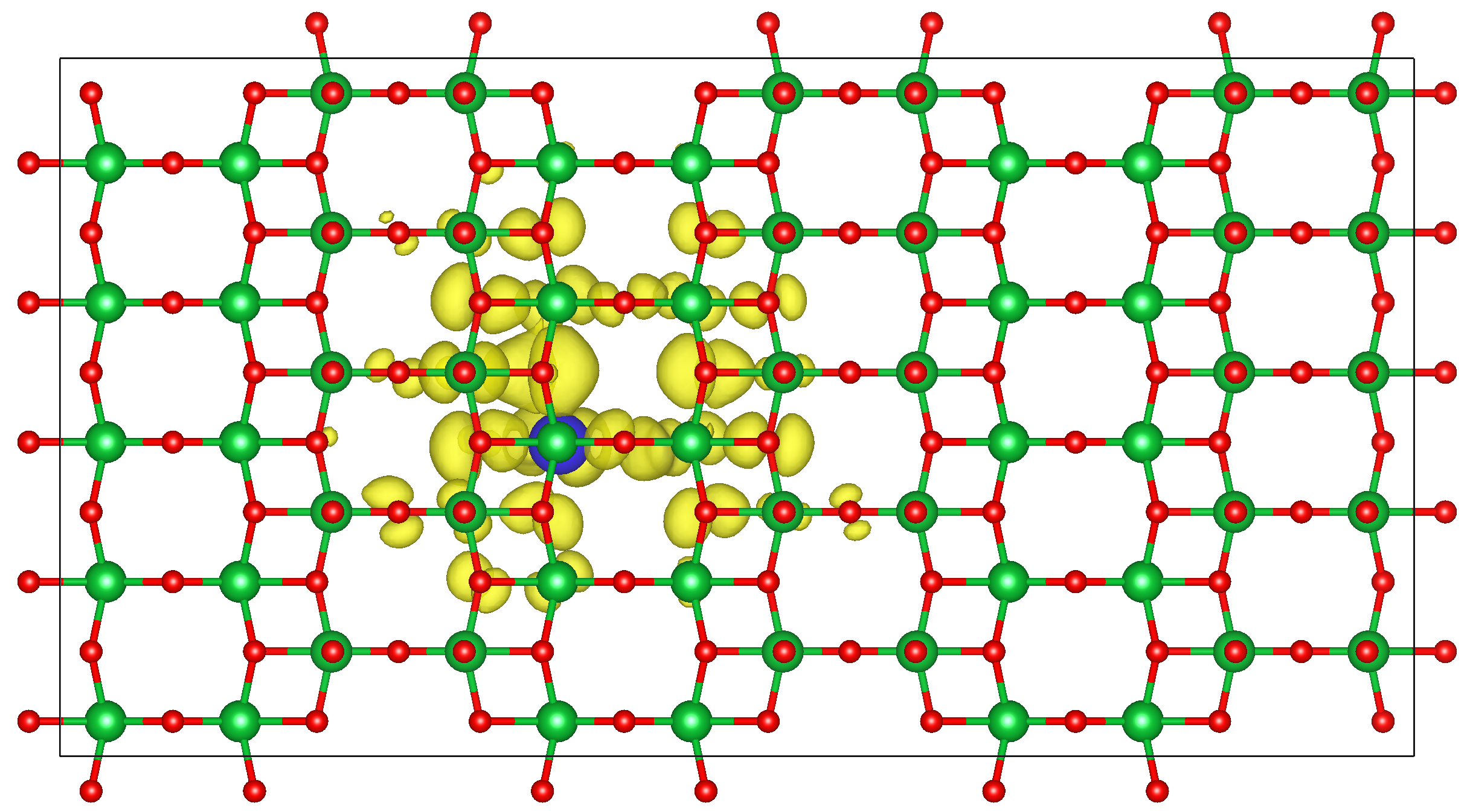
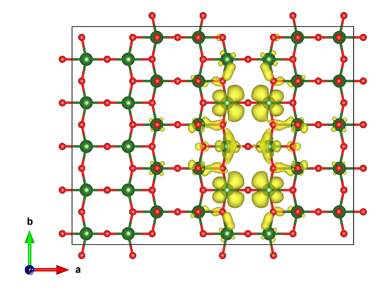
We study the composition of the excitons in various ways. First, we show the bands that contribute significantly to a given exciton by selecting a narrow energy window containing just one exciton eigenvalue and by plotting as a color weight on the band plot, where the sum is over , when plotting the weight on the valence band . Similarly, gives the weight on the conduction bands. These are shown in the first row of Fig. 5(a-c) for different excitons of interest. Next, in , we can expand the Bloch functions into the muffin-tin orbital basis functions in a Mulliken analysis, and sum these over angular momenta per atom to obtain a contribution per atom and hence per atom pair of the exciton. The superscript indicates the hole or electron atom location. This is a fully real space analysis. In other words, an inverse Fourier sum is applied to the LMTO basis Bloch functions depending on the k-mesh used. For a k-mesh, we obtain contributions in a supercell in real space. We select the most important contributions and indicate them as a percentage on a pie-chart in the second row (d-f). For example V-O means all contributions from an electron on a V and a hole on an Oc regardless of the relative position of the two atoms. Third, we can pick a location for the hole and then display the probability to find the electron around it as a isosurface or fix the electron and visualize the hole distribution. We here analyze the dark exciton at 2.65 eV, the bright exciton at 3.1 eV and then the 3.2 eV exciton from left to right.
First, from the band weight plots, we can see that all three excitons are derived primarily from the top valence band and lowest conduction band with some smaller contributions from bands farther away from the band edges. They are very spread out in k-space, and hence localized in real space. The localization in real space depends somewhat on the arbitrary choice of isosurface value cut-off which we pick around 10 %. Nonetheless they are spread in real space over a few neighbor distances in each direction. One can see from the band plots that the exciton weights are slightly different for the three excitons. For example, the exciton had a stronger contribution from and lines while the exciton has larger contributions from . The dark exciton is even more equally spread in k-space and hence even more localized in real space. This is consistent with a similar analysis by Gorelovet al. [2].
The atom pair analysis shows that the exciton weights stem primarily from electrons on V and holes on the various O. This is consistent with the band analysis, since the lowest conduction bands are V-O antibonding states and have primarily V- content, while the top valence bands are V-O bonding states and have primarily O- content. It is interesting that the different O do not contribute equally. For the dark exciton, the primary contribution is from the Ob 40% with a small contribution from chain oxygens 9 % and 30 % of the vanadyl O. This distribution occurs in spite of the fact that each V has one Ov, three Oc neighbors and only one Ob is shared by two V across a bridge. For the bright excitons, instead we see primarily contribution around 40% from the chain O and only a small contribution (about 16 % and 6 % for and directions respectively) from the bridge O and and around 21–26 % of the vanadyl oxygen.
We next show the real space figures for each exciton when the hole is fixed on Ob, Oc and Ov and when the electron is fixed on V. We can compare the 3.1 and 2.65 eV excitons for the hole fixed on the bridge O with the work of Gorelov et al. [2]. In that paper the exciton appeared more extended in the a direction perpendicular to the chains, and a simple tight-binding model with exciton wave functions centered on the V-Ob-V bridge was developed to understand their spread, comparing in particular the dark and the bright exciton for as even and odd partners to each other in their and components. In retrospect that model, while instructive, may be somewhat oversimplified.[36].
One might ask to what extent the real space distributions are sensitive to the precise location of the fixed hole (or electron). The code used to make these figures snaps the position we give as input to the nearest grid point in the real space mesh and this can sometimes be slightly off from the more symmetric atom position we target. For example, Fig. 5(i) appears to have the electron distribution skewed to the right of the bridge O. Nonetheless in (g) and (h) we choose the exact same hole location and yet these appear more symmetric. On the other hand, in (k) and (l) we use the same Oc position and yet for the 3.1 eV exciton the wave function spreads more the the left and for the 3.2 eV one more to the right. In view of their different k-space localization, these appear to be genuine differences between these excitons and not just artifacts of the precise location of the fixed particle in the exciton and we further tested that they are robust to small displacements of the assumed hole position. Complementary information is gained by fixing the electron on a V and examining the corresponding hole distribution. These are show in part (p-r) of Fig. 5 In these figures we can recognize the O- like character, while in the previous ones, we can recognize the like character on V.
The consistent picture that emerges from these various visualizations is that the dark exciton at 2.65 eV is significantly more localized than the two bright excitons considered here. They have a rather complex distribution spread over a size of about 5-15 Å and are charge transfer like excitons. Overall, these examples confirm the main finding from Gorelov et al. [2] that the excitons are not Frenkel excitons, which one might expect to stay localized on a single atom or molecular fragment like the V-Ob-V bridge, but are more spread out than one would expect for such large exciton binding energies. However, they are more complex than previously thought. Similar strongly anisotropic (almost unidirectional) and strongly bound excitons have been observed in the puckered two-dimensional magnet CrBrS [37, 38]. Much as the strongly bound excitons in V2O5 those excitons also extend up to 3-4 unit cells. However, in strong contrast to the excitons in V2O5, excitons in CrBrS originate from partially filled -states and are magnetic in nature and have both large on-site and significant inter-site dipole characters [39] to them. The V2O5 excitons, however, have barely any onsite components and mostly share the electrons and holes on the V-O () dipole. In other words, as already pointed out by Gorelov et al. [2] they can be viewed as charge-transfer excitons. It is in that sense that these excitons are significantly different from Frenkel excitons as observed in several strongly correlated ferro- and anti-ferromagnets[40, 41].
III.2 Monolayer
III.2.1 Quasiparticle and optical gaps
Having established good agreement with prior work for V2O5 in spite of some differences, we move on to study the monolayer. To calculate the monolayer, we simply increase the distance between the V2O5 layers by increasing the -lattice constant and keeping the layer atomic positions fixed. Using the coordinate difference between the vanadyl oxygens sticking out on either side of the layer as a measure of the thickness of the layer, the layer has a thickness of 4.096 Å. The c lattice constant is 4.368 Å and the V-Ov vertical distance is 1.575 Å, so between the Ov of one layer and the V above it in the next layer, the distance is 2.793 Å. When we set the the vacuum thickness is 7.416 Å and the distance from the Ov to the next layer V is 9.9Å. Using the vacuum layer is 13.17Å and the vertical distance from the Ov to the V above it is 15.69 Å. These seem sufficiently large to represent well isolated monolayers. The band structure of the monolayer using is shown in Fig. 6. To check the convergence we plot the direct and indirect band gaps as function of in Fig. 7.
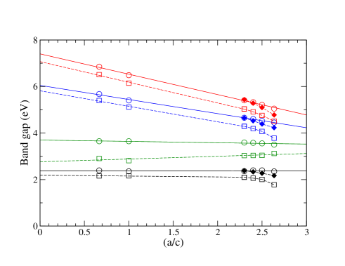
The band structure plot Fig. 6 shows that already at the GGA level, the indirect gap is slightly increased compared to the bulk, primarily because the highest valence band in the plane (at ) is now almost the same as in the plane (at ). The upward dispersion from in the bulk case is missing. This indicates that this dispersion is related to the interlayer hopping interaction in the bulk. Several changes happen in the band structure: the smallest direct gap, which in bulk occurs at now occurs at because the bands along the direction become flat. Secondly, the indirect gap, which in bulk occurs between the VBM at or near and the CBM at now shifts to a point between X-S and . The self-energy shifts are significantly higher than in the bulk.
In Fig. 7, we can see that these changes occur as soon as the layers become decoupled already for a modest increase in interlayer distance (=2.3 or =5 Å). The smallest direct gap becomes equal to the direct gap at and in the GGA, the band gaps have essentially converged at this point and stay constant. On the other hand, the QS and QS gaps keep on increasing linearly as we further increase . This slow convergence with the size of the vacuum region is caused by the long-range nature of the self-energy which is proportional to the screened Coulomb interaction because of the screened exchange term. With increasing size of the vacuum the effective dielectric constant of the system becomes smaller. Effectively, the long-range part of the Coulomb interaction becomes unscreened and dominated by the vacuum or surrounding medium for a thin 2D system. This is well known since the work of Keldysh [25] and discussed in detail in Cudazzo et al. [24]. The monolayer is thus predicted to have a significantly higher gap than bulk layered V2O5. The extrapolated direct quasiparticle gaps are 7.4 eV and 6.1 eV in the QS and QS approximations. The difference between direct and indirect gap stays approximately constant as we increase . Also, the difference between QS and QS stays more or less constant.
On the other hand, the BSE optical gap stays almost constant. The lowest optical gap shown in Fig. 7 is for and is a mixture of various direct interband transitions spread throughout k-space. It is not dominated by the lowest gap direct gap (which is at in the bulk case) as we have seen in Fig. 5. It does not show the initial increase of the direct and indirect gaps as we start increasing . It also does not increase as the QS gaps. This is because the exciton binding energy is also proportional to and hence an increase in due to lower screening results both in an increased self-energy and quasiparticle gap but compensating an increased exciton binding energy. The optical gap is thus expected to change only minimally. This applies both when we use or . In the latter case, the gap seems to go slightly down for larger , but this is within the error bar. It might indicate that the increase in with is more directly reflected in the exciton binding energy than in the quasiparticle self-energy. This also implies that the exciton gap will be less affected by substrate dielectric screening if the monolayer is placed on top of a substrate. We can however expect that an indirect exciton (not calculated here) would show the initial increase related to the changes in band structure but then quickly settle and become constant. We can see that the change between indirect gap in bulk and the isolated monolayer is or order a few 0.1 eV.
Next we show the dielectric function for the monolayer in Fig. 8. We can now see an even stronger suppression of the in the BSE for . Again, at higher energies, sharp features occur for the polarization perpendicular to the layers but these are dismissed as unrealistic artifacts from the BSE active space truncation. This indicates that the local field effects are even stronger in the monolayer case. The excitons are still prominent for the in-plane polarizations, but the lowest peaks still occur near 3.0 eV not too far from the bulk case. Still, the shape of the , i.e. the exciton spectrum, is significantly different from the bulk case.
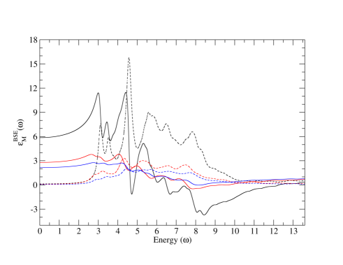
Next, we look a little more closely at the change in dielectric functions as function of interlayer spacing in Fig. 9. We can see first of all that the amplitude of the and the values of are much reduced in the monolayer cases compared to the bulk and increasingly more so as the thickness of the vacuum layer increases. This can simply be understood in terms of a model of capacitors in series. Essentially, there is a thicker and thicker region of relative dielectric constant in between the layers. Since the capacitance is inversely proportional to its thickness and proportional to the dielectric constant in that region, the effective dielectric constant can be obtained from adding the capacitance of the layer and of the vacuum region in series, which gives
| (7) |
where is the -lattice constant for bulk and the one in the monolayer model. In the limit this goes to 1, the dielectric constant of vacuum, and in the limit it gives of bulk V2O5
The real space spread of the first bright exciton for in the monolayer is shown in Fig. 10. It looks quite similar to that in the bulk case, except that it is of course entirely confined to one monolayer. Its spread in and direction appear slightly larger here than in Fig. 5(h) but this is because we here used a mesh. Apparently two k-points in the a direction is not yet sufficient to avoid overlap of the excitons in adjacent cells from the periodic boundary conditions in the a direction.
III.2.2 Comparison to experiment
Monolayer V2O5 has not yet been realized although attempts at exfoliation have resulted in ultrathin layers of order 8-10 atomic layers thick.[42] Only recently, layers as thin as bi- or trilayer of V2O5 were realized by sonification after swelling of the interlayer distance by intercalation with formamide molecules as reported by Reshma et al. [43]. These studies showed an increase in optical absorption edge by about 1.3 eV for the thinnest samples which contained individual layers of order 1.1-1.5 nm, corresponding to 2-3 layers. It is not straightforward to interpret the onset of the Tauc plot as the direct gap because of the large excitonic effects and disorder related band tailing effects. The Tauc plot prediction of an absorption coefficient proportional to for direct allowed transitions is valid only for band to band transitions. However, including polaritonic effects it may also correspond to indirect excitons [44]. The value reported for bulk in [43] is 2.39 eV, which is close to the gap reported by Kenny and Kannewurf[4] but much smaller than the direct excitonic peak seen in spectroscopic ellipsometry [2]. See also Fig. 3. Thus, the Tauc-plot onsets more likely correspond to an indirect exciton but may also be influenced by defects. While the direct exciton gap is not expected to vary significantly with layer separation according to our present calculations, because such excitons are a mixture of band to band transitions at different k-points, and because of the compensation of exciton binding energy and gap shift, the indirect gap exciton might have a somewhat higher binding energy and be more localized in k-space. For the bulk we obtain a lowest direct gap at 4.2 eV and the lowest bright exciton is at 3.1 eV, indicating an exciton binding energy of eV. Assuming that an indirect exciton associated with the indirect gap of 3.8 eV has a similar binding energy, we would find the optical indirect exciton gap in bulk at about 2.7 eV. This is still 0.3 eV larger than the onset of the Tauc plot in [43]. Thus we hypothesize that the exciton binding energy is larger for the indirect exciton. Nonetheless, we might expect the indirect exciton to more closely follow a specific band edge and thus increase slightly with increasing layer separation. Furthermore the nature of the indirect transition changes to another k-location of the VBM and the difference between direct and indirect quasiparticle gap is reduced from that in bulk. Similar changes in direct/in-direct nature of the band gap going from the bulk to the monolayer limit are observed in several layered vdW systems [45, 46]. We may thus expect that for monolayers the optical gap even if still indirect might approach more closely the direct gap exciton. Still our calculations of the indirect band gap shift between bulk an monolayer indicate this shift would be of only 0.3 eV or so, which is significantly smaller than what is reported in [43]. To better understand this discrepancy it will be necessary to calculate indirect exciton gaps and to obtain a more detailed experimental analysis of monolayer optical properties.
IV Conclusions
In this paper we presented all-electron quasiparticle band structure calculations using a modified QS method, and optical response function calculations using the BSE approach. The inclusion of ladder diagrams in calculating the polarization function which determines the screened Coulomb interaction of the method is shown to reduce the self-energy by about a factor 0.77. Our quasiparticle band gaps for the bulk including these electron-hole effects are in good agreement with the literature using a pseudopotential implementation but without this electron-hole reduction of the . Because of this somewhat fortuitous agreement on the quasiparticle gap, in spite of the different approximations made in the calculation of , we then find the excitons and imaginary part of the dielectric function to also be in good agreement with prior work for bulk. There thus remains some discrepancy on how to obtain the correct but once is established, good agreement is obtained in band structures and optical dielectric response. Some effects of the strong local field effects in the direction perpendicular to the layers were observed here and the appearance of unphysical high energy sharp peaks was shown to be an artifact of the truncation of the active space in the BSE. Finally, the electronic screening only static dielectric constant was evaluated using an extrapolation from finite q and found to give good agreement for the indices of refraction with experiment to within about 15 %. This confirms that in the QS approach both the band gaps and the screening are consistently in good agreement with experiment.
For monolayers, we find an increased quasiparticle gap but slow convergence of the quasiparticle gap with the distance between the layers, as observed in other 2D systems. On the other hand, the optical direct exciton gap converges much faster because as the quasiparticle gap increases, so increases the exciton binding energy because both are proportional to , which is increased by reduced screening in a 2D system. The local field effect perpendicular to the layer were found to be even stronger in the monolayer than in the bulk. While the direct gap at does not change much between bulk and monolayer at the GGA level, the top valence band becomes flattened out and this increases both the smallest direct gap at and the indirect gap. Assuming a similar exciton binding energy for the (not yet calculated) indirect exciton as for the direct excitons, we predict a slight increase of the optical absorption onset in monolayers. An increase in optical gap was recently observed for exfoliated 2-3 layer thin samples but was found to exhibit larger shifts than we here predict.
Data Availability: The data pertaining to various figures are available at https://github.com/Electronic-Structure-Group/v2o5-quasiparticle-exciton.
Acknowledgements.
This work was supported by the U. S. Department of Energy Basic Energy Sciences (DOE-BES) under Grant No. DE-SC0008933. Calculations made use of the High Performance Computing Resource in the Core Facility for Advanced Research Computing at Case Western Reserve University. S.A. is supported by the Computational Chemical Sciences program within the U.S. DOE, Office of Science, BES, under award no. DE-AC36-08GO28308. S.A. used resources of the National Energy Research Scientific Computing Center, a DOE Office of Science user facility supported under award no. DE-AC02-05CH11231 using NERSC award BES-ERCAP0021783. We thank Vitaly Gorelov and co-authors of ref. 2 for providing the numerical data of their calculations and for useful discussions. We also thank Dimitar Pashov for his many contributions to the codes used here.Appendix A Discussion of sharp high energy features in in BSE
(a) 
(b) 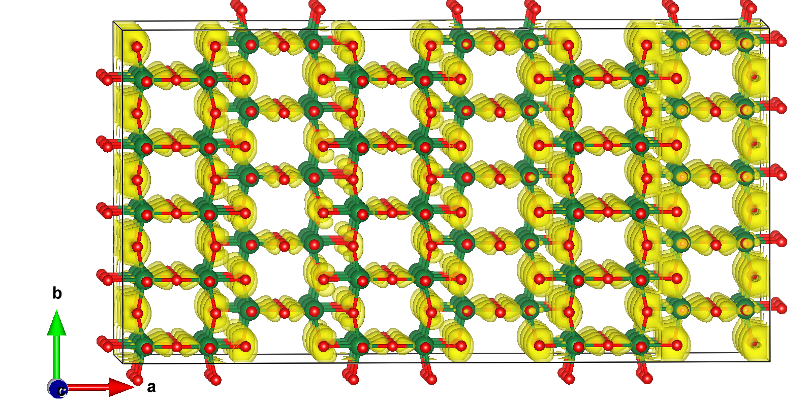
In the main text in Fig. 3 sharp features appear at high energy for . That calculation was done with 30 valence bands and 20 conduction bands. Looking at an even wider energy range than in the main paper, it appears that not only is there a feature at 13.5 eV but peaks also appear at 18 eV and 26 eV. If we include 30 instead of 20 conduction bands, the 13.5 eV and 18 eV features disappear or at least are strongly reduced in intensity as shown here in Fig. 11. However, we can see that the 26 eV feature is still there. In the region below 10 eV the is somewhat less suppressed indicating that some redistribution of oscillator strength from these high energy features to the lower energy region takes place by mixing more bands in the BSE active space. Furthermore, when we examine which bands contribute to the peak in in the energy range of the 13.5 eV peak, we find it is strongly derived from the lowest O- band and the topmost V- band. See Fig. 12. In fact, within the active space of , and these are the only bands which can give an energy band difference in this energy range. When 30 conduction bands are included, the band analysis still indicates a strong contribution from the bottom O- bands but in the conduction band it is no longer localized near the top of the -bands. Instead the weight is distributed over many bands. This spreading out of the oscillator strengths is related to the transitions to strongly dispersing free-electron-like bands above the V- conduction bands for . This extreme dependence on the truncation of the active space of bands included, indicates that these sharp features at high energy are artifacts of the truncation of the active space in the BSE calculation. To obtain reliable results at increasingly higher energies would require one to increase the size of the active space accordingly. For example, the peak near 26 eV also becomes reduced when is increased from 30 to 40 so as to include the O- contributions.
We also examine the changes between and for the two-particle distribution in real space. When we place the hole on a bridge Ob this wave function is found to be fairly localized to its V neighbors and nearby O-V bonds as shown in Fig. 13a for the case. On the other hand, when is increased to 30, the wave function becomes very delocalized as shown in Fig. 13(b).
As mentioned in the main text, there is no compelling reason to focus on the hole at the Ob. In fact, the bottom O- bands near eV correspond to -bonds from various oxygen types. Fig. 14 shows that for the calculation, when we place the electron on V and examine the hole distribution, not only the nearest bridge Ob has a strong contribution but there are also strongly localized contributions on the vanadyl Ov, both the one bonded directly to the V on which the electron is placed and the one in the adjacent layer. There are also quite delocalized contributions on the V-Oc -bonds in the double zigzag chains. So, while this sharp peak at 13.5 eV has some localized aspects in terms of its two particle electron-hole wave function, it also has delocalized aspects. In any case, it shows a strong inhomogeneity in the direction perpendicular to the layers, which we can associate with a strong local field effect.
It remains curious that we only see these high energy features for the direction perpendicular to the layers, which suggests a connection to strong local field effects. Inspecting the eigenvalues of the two-particle Hamiltonians, we do find eigenvalues up to 26 eV for the case, indicating that the matrix elements of the local field part of the kernel , which are positive unlike those of can significantly increase the eigenvalues beyond and lead to spurious peaks in the . This indicates indeed that the higher peaks at and 25 eV are also related to local field effects.
(a) 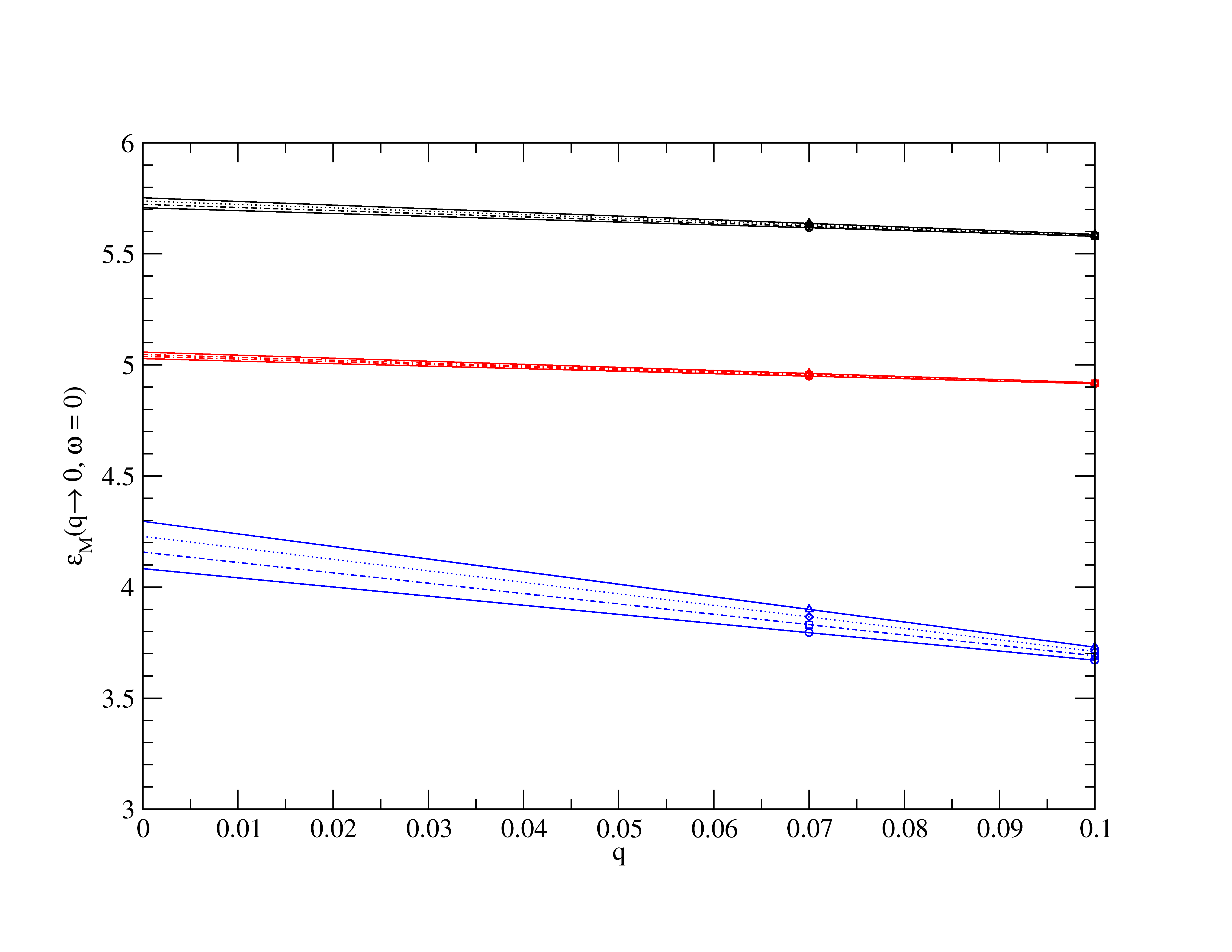
(b) 
| ( 0, , = 0) | ( 0, , = 0) | |||||
| VTF | Ea | Eb | Ec | Ea | Eb | Ec |
| 6.0e-5 | 3.5947 | 3.4014 | 3.3019 | 5.7071 | 5.0282 | 4.0831 |
| 7.0e-5 | 3.6044 | 3.4096 | 3.3457 | 5.7235 | 5.0383 | 4.1577 |
| 8.0e-5 | 3.6135 | 3.4174 | 3.3872 | 5.7376 | 5.0480 | 4.2285 |
| 9.0e-5 | 3.6222 | 3.4248 | 3.4264 | 5.7521 | 5.0575 | 4.2963 |
| ( = 0, 0, = 0) | ( = 0, 0, = 0) | |||||
| 3.5400 | 3.3548 | 3.0541 | 5.6183 | 4.9698 | 3.6586 | |
| ntheo | 1.88 | 1.83 | 1.75 | 2.37 | 2.23 | 1.91 |
| nexp | 2.07 | 2.12 | 1.97 | |||
Appendix B Extrapolating to
Here we discuss some details of the finite procedure to calculate the static dielectric constant. As mentioned in the main text, the bare Coulomb interaction is repaced by a Thomas Fermi screened one to avoid numerical difficulties near . The limit must be treated carefully because has an integrable divergence , which is handled in the Questaal codes by means of the offset- method and by replacing the bare Coulomb interaction by with a small . Values of , are chosen between 6 and and we then extrapolate first to zero for different and subseuently to zero. We find that for the direction the results depend more sensitively on the choice of and hence a larger uncertainty results on the extrapolated results than for the and directions. Furthermore, using too small values of either or can lead to unphysical results because of numerical artifacts. The extrapolation of the BSE results is shown in Fig. 15. The top part shows the extrapolation as function of for different values and the bottom the extrapolation vs. . The data used in these plots and the linear extrapoaltion results are given in Table 3.
References
- Radha et al. [2021] S. K. Radha, W. R. L. Lambrecht, B. Cunningham, M. Grüning, D. Pashov, and M. van Schilfgaarde, Optical response and band structure of including electron-hole interaction effects, Phys. Rev. B 104, 115120 (2021).
- Gorelov et al. [2022] V. Gorelov, L. Reining, M. Feneberg, R. Goldhahn, A. Schleife, W. R. L. Lambrecht, and M. Gatti, Delocalization of dark and bright excitons in flat-band materials and the optical properties of V2O5, npj Computational Materials 8, 94 (2022).
- Eyert and Höck [1998] V. Eyert and K.-H. Höck, Electronic structure of : Role of octahedral deformations, Phys. Rev. B 57, 12727 (1998).
- Kenny et al. [1966] N. Kenny, C. Kannewurf, and D. Whitmore, Optical absorption coefficients of vanadium pentoxide single crystals, Journal of Physics and Chemistry of Solids 27, 1237 (1966).
- Bhandari et al. [2015] C. Bhandari, W. R. L. Lambrecht, and M. van Schilfgaarde, Quasiparticle self-consistent calculations of the electronic band structure of bulk and monolayer , Phys. Rev. B 91, 125116 (2015).
- Lany [2013] S. Lany, Band-structure calculations for the 3d transition metal oxides in GW, Phys. Rev. B 87, 85112 (2013).
- van Setten et al. [2017] M. J. van Setten, M. Giantomassi, X. Gonze, G.-M. Rignanese, and G. Hautier, Automation methodologies and large-scale validation for : Towards high-throughput calculations, Phys. Rev. B 96, 155207 (2017).
- Mokerov et al. [1976] V. G. Mokerov, V. L. Makarov, V. B. Tulvinskii, and A. R. Begishev, Optical properties of vanadium pentoxide in the region of photon energies from 2 eV to 14 eV, Optics and Spectroscopy 40, 58 (1976).
- Losurdo et al. [2000] M. Losurdo, G. Bruno, D. Barreca, and E. Tondello, Dielectric function of V2O5 nanocrystalline films by spectroscopic ellipsometry: Characterization of microstructure, Applied Physics Letters 77, 1129 (2000).
- Gorelov et al. [2023] V. Gorelov, L. Reining, W. R. L. Lambrecht, and M. Gatti, Robustness of electronic screening effects in electron spectroscopies: Example of , Phys. Rev. B 107, 075101 (2023).
- Kotani et al. [2007] T. Kotani, M. van Schilfgaarde, and S. V. Faleev, Quasiparticle self-consistent GW method: A basis for the independent-particle approximation, Phys.Rev. B 76, 165106 (2007).
- Pashov et al. [2019] D. Pashov, S. Acharya, W. R. Lambrecht, J. Jackson, K. D. Belashchenko, A. Chantis, F. Jamet, and M. van Schilfgaarde, Questaal: A package of electronic structure methods based on the linear muffin-tin orbital technique, Computer Physics Communications , 107065 (2019).
- Friedrich et al. [2010] C. Friedrich, S. Blügel, and A. Schindlmayr, Efficient implementation of the approximation within the all-electron FLAPW method, Phys. Rev. B 81, 125102 (2010).
- Kutepov [2016] A. L. Kutepov, Electronic structure of Na, K, Si, and LiF from self-consistent solution of Hedin’s equations including vertex corrections, Phys. Rev. B 94, 155101 (2016).
- Kutepov [2017] A. L. Kutepov, Self-consistent solution of Hedin’s equations: Semiconductors and insulators, Phys. Rev. B 95, 195120 (2017).
- Kutepov [2022] A. L. Kutepov, Full versus quasiparticle self-consistency in vertex-corrected GW approaches, Phys. Rev. B 105, 045124 (2022).
- Jiang and Blaha [2016] H. Jiang and P. Blaha, with linearized augmented plane waves extended by high-energy local orbitals, Phys. Rev. B 93, 115203 (2016).
- Cunningham et al. [2018] B. Cunningham, M. Grüning, P. Azarhoosh, D. Pashov, and M. van Schilfgaarde, Effect of ladder diagrams on optical absorption spectra in a quasiparticle self-consistent framework, Phys. Rev. Materials 2, 034603 (2018).
- Cunningham et al. [2023] B. Cunningham, M. Grüning, D. Pashov, and M. van Schilfgaarde, : Quasiparticle self-consistent with ladder diagrams in , Phys. Rev. B 108, 165104 (2023).
- Shishkin et al. [2007] M. Shishkin, M. Marsman, and G. Kresse, Accurate Quasiparticle Spectra from Self-Consistent GW Calculations with Vertex Corrections, Phys. Rev. Lett. 99, 246403 (2007).
- Chen and Pasquarello [2015] W. Chen and A. Pasquarello, Accurate band gaps of extended systems via efficient vertex corrections in , Phys. Rev. B 92, 041115(R) (2015).
- Hedin [1965] L. Hedin, New method for calculating the one-particle green’s function with application to the electron-gas problem, Phys. Rev. 139, A796 (1965).
- Hedin and Lundqvist [1969] L. Hedin and S. Lundqvist, Effects of electron-electron and electron-phonon interactions on the one-electron states of solids, in Solid State Physics, Advanced in Research and Applications, Vol. 23, edited by F. Seitz, D. Turnbull, and H. Ehrenreich (Academic Press, New York, 1969) pp. 1–181.
- Cudazzo et al. [2011] P. Cudazzo, I. V. Tokatly, and A. Rubio, Dielectric screening in two-dimensional insulators: Implications for excitonic and impurity states in graphane, Phys. Rev. B 84, 085406 (2011).
- Keldysh [1979] L. V. Keldysh, Coulomb interaction in thin semiconductor and semimetal films, Soviet Journal of Experimental and Theoretical Physics Letters 29, 658 (1979).
- Perdew et al. [1996] J. P. Perdew, K. Burke, and M. Ernzerhof, Generalized Gradient Approximation Made Simple, Phys. Rev. Lett. 77, 3865 (1996).
- Starke and Kresse [2012] R. Starke and G. Kresse, Self-consistent Green function equations and the hierarchy of approximations for the four-point propagator, Phys. Rev. B 85, 075119 (2012).
- Maggio and Kresse [2017] E. Maggio and G. Kresse, GW Vertex Corrected Calculations for Molecular Systems, Journal of Chemical Theory and Computation 13, 4765 (2017).
- Enjalbert and Galy [1986] R. Enjalbert and J. Galy, A refinement of the structure of V2O5, Acta Crystallographica Section C 42, 1467 (1986).
- Bhandari et al. [2018] C. Bhandari, M. van Schilfgaarde, T. Kotani, and W. R. L. Lambrecht, All-electron quasiparticle self-consistent band structures for including lattice polarization corrections in different phases, Phys. Rev. Mater. 2, 013807 (2018).
- Hybertsen and Louie [1987] M. S. Hybertsen and S. G. Louie, Ab initio static dielectric matrices from the density-functional approach. i. formulation and application to semiconductors and insulators, Phys. Rev. B 35, 5585 (1987).
- Onida et al. [2002] G. Onida, L. Reining, and A. Rubio, Electronic excitations: density-functional versus many-body green’s-function approaches, Rev. Mod. Phys. 74, 601 (2002).
- Del Sole and Girlanda [1993] R. Del Sole and R. Girlanda, Optical properties of semiconductors within the independent-quasiparticle approximation, Phys. Rev. B 48, 11789 (1993).
- [34] XCrysDen is a crystal structure and density visualizaiton program available at http://www.xcrysden.org.
- [35] VESTA is a 3D visualization program for structural models and volumetric data available from https://jp-minerals.org/vesta/en/.
- [36] Vitaly Gorelov and Lucia Reining pointed out to us in private communication that they carried out a revised analysis of the exciton spread, which now appears to be similar in the directions perpendicular and parallel to the chains and is closer to our present results.
- Klein et al. [2023] J. Klein, B. Pingault, M. Florian, M.-C. Heißenbüttel, A. Steinhoff, Z. Song, K. Torres, F. Dirnberger, J. B. Curtis, M. Weile, A. Penn, T. Deilmann, R. Dana, R. Bushati, J. Quan, J. Luxa, Z. Sofer, A. Alú, V. M. Menon, U. Wurstbauer, M. Rohlfing, P. Narang, M. Lončar, and F. M. Ross, The Bulk van der Waals Layered Magnet CrSBr is a Quasi-1D Material, ACS Nano 17, 5316 (2023).
- Shao et al. [2024] Y. Shao, F. Dirnberger, S. Qiu, S. Acharya, S. Terres, E. Telford, D. Pashov, B. S. Y. Kim, F. Ruta, D. G. Chica, Y. Wang, Y. J. Bae, A. J. Millis, M. I. Katsnelson, K. Mosian, Z. Sofer, A. Chernikov, M. v. Schilfgaarde, X. Zhu, X. Roy, and D. N. Basov, Magnetically confined surface and bulk excitons in a layered antiferromagnet (2024), unpublished.
- Ruta et al. [2023] F. L. Ruta, S. Zhang, Y. Shao, S. L. Moore, S. Acharya, Z. Sun, S. Qiu, J. Geurs, B. S. Kim, M. Fu, et al., Hyperbolic exciton polaritons in a van der Waals magnet, Nature Communications 14, 8261 (2023).
- Acharya et al. [2022] S. Acharya, D. Pashov, A. N. Rudenko, M. Rösner, M. v. Schilfgaarde, and M. I. Katsnelson, Real-and momentum-space description of the excitons in bulk and monolayer chromium tri-halides, npj 2D Materials and Applications 6, 1 (2022).
- Acharya et al. [2023] S. Acharya, D. Pashov, C. Weber, M. van Schilfgaarde, A. I. Lichtenstein, and M. I. Katsnelson, A Theory for Colors of Strongly Correlated Electronic Systems, Nat Commun 14, 5565 (2023).
- Sucharitakul et al. [2017] S. Sucharitakul, G. Ye, W. R. L. Lambrecht, C. Bhandari, A. Gross, R. He, H. Poelman, and X. P. A. Gao, V2O5: A 2D van der Waals Oxide with Strong In-Plane Electrical and Optical Anisotropy, ACS Applied Materials & Interfaces 9, 23949 (2017), pMID: 28677951.
- P. R. et al. [2021] R. P. R., A. Pazhedath, S. K. Sinha, A. Dasgupta, G. Karuppiah, A. K. Prasad, and S. Dhara, Electronic and Vibrational Decoupling in Chemically Exfoliated Bilayer Thin Two-Dimensional V2O5, The Journal of Physical Chemistry Letters 12, 9821 (2021), pMID: 34605658.
- Elliott [1957] R. J. Elliott, Intensity of Optical Absorption by Excitons, Phys. Rev. 108, 1384 (1957).
- Wu et al. [2019] M. Wu, Z. Li, T. Cao, and S. G. Louie, Physical origin of giant excitonic and magneto-optical responses in two-dimensional ferromagnetic insulators, Nature communications 10, 2371 (2019).
- Acharya et al. [2021] S. Acharya, D. Pashov, B. Cunningham, A. N. Rudenko, M. Rösner, M. Grüning, M. van Schilfgaarde, and M. I. Katsnelson, Electronic structure of chromium trihalides beyond density functional theory, Physical Review B 104, 155109 (2021).