Surface-near domain engineering in multi-domain x-cut lithium niobate tantalate mixed crystals
Abstract
Lithium niobate and lithium tantalate are among the most widespread materials for nonlinear, integrated photonics. Mixed crystals with arbitrary Nb-Ta ratios provide a new degree of freedom to tune materials properties, such as the birefringence, but also leverage the advantages of the singular compounds, for example, by combining the thermal stability of lithium tantalate with the larger nonlinear or piezoelectric constants of lithium niobate. Periodic poling is the prerequisite for any nonlinear optical application. For mixed crystals this has been challenging so far due to the lack of homogeneous, mono-domain crystals, which severely inhibit domain growth and nucleation. In this work we demonstrate that surface-near ( m depth) periodic poling on x-cut lithium niobate tantalate mixed crystals can be achieved via electric field poling and lithographically structured electrodes. We find that naturally occurring head-to-head or tail-to-tail domain walls in the as-grown crystal inhibit domain inversion at a larger scale. However, periodic poling is possible, if the gap size between the poling electrodes is of the same order of magnitude or smaller than the average size of naturally occurring domains. This work provides the basis for the nonlinear optical application of lithium niobate tantalate mixed crystals.
Integrated quantum photonics exploits (second-order) nonlinear optical effects for many applications ranging from single photon generation, filtering, signal analysis, amplification or as interconnects between quantum systems operating in different wavelength regimes [1, 2, 3, 4, 5, 6]. Lithium niobate (LiNbO3, LNO) and lithium tantalate (LiTaO3, LTO) are widely used for nonlinear optical applications due to their large nonlinear optical coefficients, easy availability of large, optical-quality wafers in form of bulk crystals or thin films, as well as a largely developed technology, which can be leveraged for fabrication [7, 8, 9, 3].
Efficient nonlinear optical processes require phase matching between the interacting beams, which can be achieved independently of the material dispersion via quasi-phase matching in periodically-poled ferroelectric domain structures in LNO or LTO [10, 9, 11]. Mixed crystals of lithium niobate and lithium tantalate (LiNb1-xTaxO3, LNTx) can be created with arbitrary Nb/Ta ratios over the full compositional range[12, 13, 14, 15, 16, 17]. They allow to interpolate between the refractive indices and dispersions of LNO and LTO, because LNO is negatively birefringent at room temperature, while LTO is positively birefringent. Thus, for a given temperature a crystal composition can be found, where the birefringence vanishes, while the crystal retains its ferroelectric polarization and nonlinearity [18]. Furthermore, LNTx mixed crystals enable the combination of favorable properties of the individual materials for designing compounds with novel features. Examples are combining the superior thermal stability of LTO, with the larger nonlinear and piezo-electrical coefficients of LNO [16, 19, 15] or the possibility to create waveguides in layered hetero-structures [14, 12].
The engineering of domains in LNTx has been challenging, because the so-far available crystals are single-crystalline but multidomain, i.e. they feature a random domain patterning along the z-axis [15, 16, 20]. Recently, it was observed that the as-grown domain pattern in LNT features non-charged 180° domain walls, which are parallel to the c-axis, but also so-called head-to-head and tail-to-tail domain wall configurations, which are oriented 90° with respect to the spontaneous polarization direction [16]. Such head-to-head or tail-to-tail domain walls are known to be highly charged [21, 22].
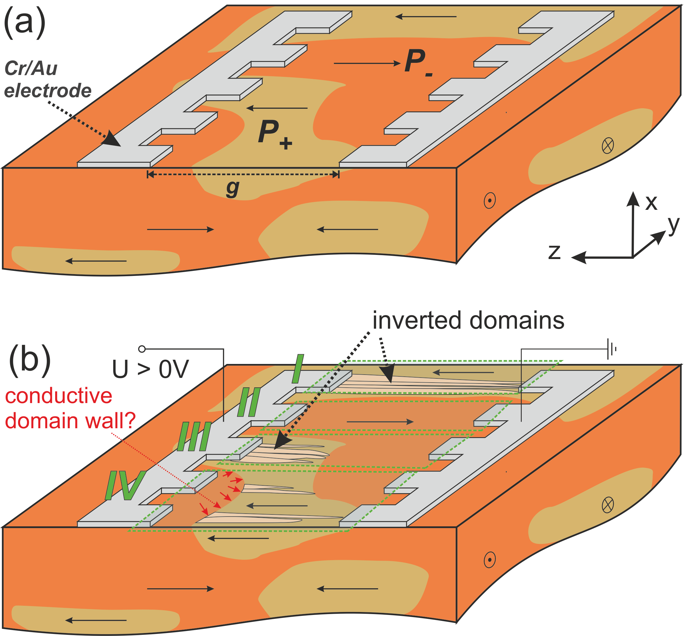
The LNTx system is a uniaxial ferroelectric, i.e. only two domain orientations are possible. They are aligned along the z-axis (crystallographic c-axis). Figure 1(a) shows a sketch of a random domain pattern in Czochralski-grown single crystals of LNTx. The average width along the z-axis of the as-grown domains for our sample are in the range of a few 10 m. It is suspected that local variations of the Ta/Nb ratio in the range of a few percent points, which naturally occur during growth [15], act as pinning center and create very stable as-grown domain patterns, which present a challenge for poling [20].
Since it is challenging to produce large, single-domain crystals [20, 16] , the poling of LNTx crystals at a local scale of a few 10 m is an alternative. This is on the same order or smaller than the original domain sizes of as-grown crystals. For applications in integrated nonlinear optics a periodic periodically-poled area with a width and depth of a few microns, because typical waveguides have at most a width of a few microns in both thin film or bulk [23, 7, 3, 11].
In this work we demonstrate that surface-near periodic poling in x-cut LNTx mixed crystals can be achieved by using lithographically structured metal electrodes across a gap and electric field poling at room temperature. By applying multiple electrical pulses with inverted polarity during the poling process, also a periodic poling can be achieved, even in an originally randomly patterned domain structure.
In this work, we analyze the surface-near domain engineering in a piece of x-cut LNTx. The crystal has been grown at the Leibniz Institut for Crystal Growth, Berlin. The crystal was oriented via x-ray diffraction, while the Nb/Ta concentration was confirmed with x-ray fluorescence spectroscopy. For our crystal, we have determined a Ta-content of . Details on the growth of the crystal and the fundamental characterization can be found elsewhere [15].
Figure 1(a) shows the principle experimental geometry for the poling geometry. We deposited chromium-gold finger electrodes with a periodic pattern of 10 m in y-direction. Multiple electrodes of 250 m length and gap distances ranging from 20 to 30 m were fabricated on different regions of the crystal. The overall poling procedure and electrode design is similar to the widely studied poling of x-cut thin film or bulk LNO [24, 25, 26, 27, 28, 29, 6].
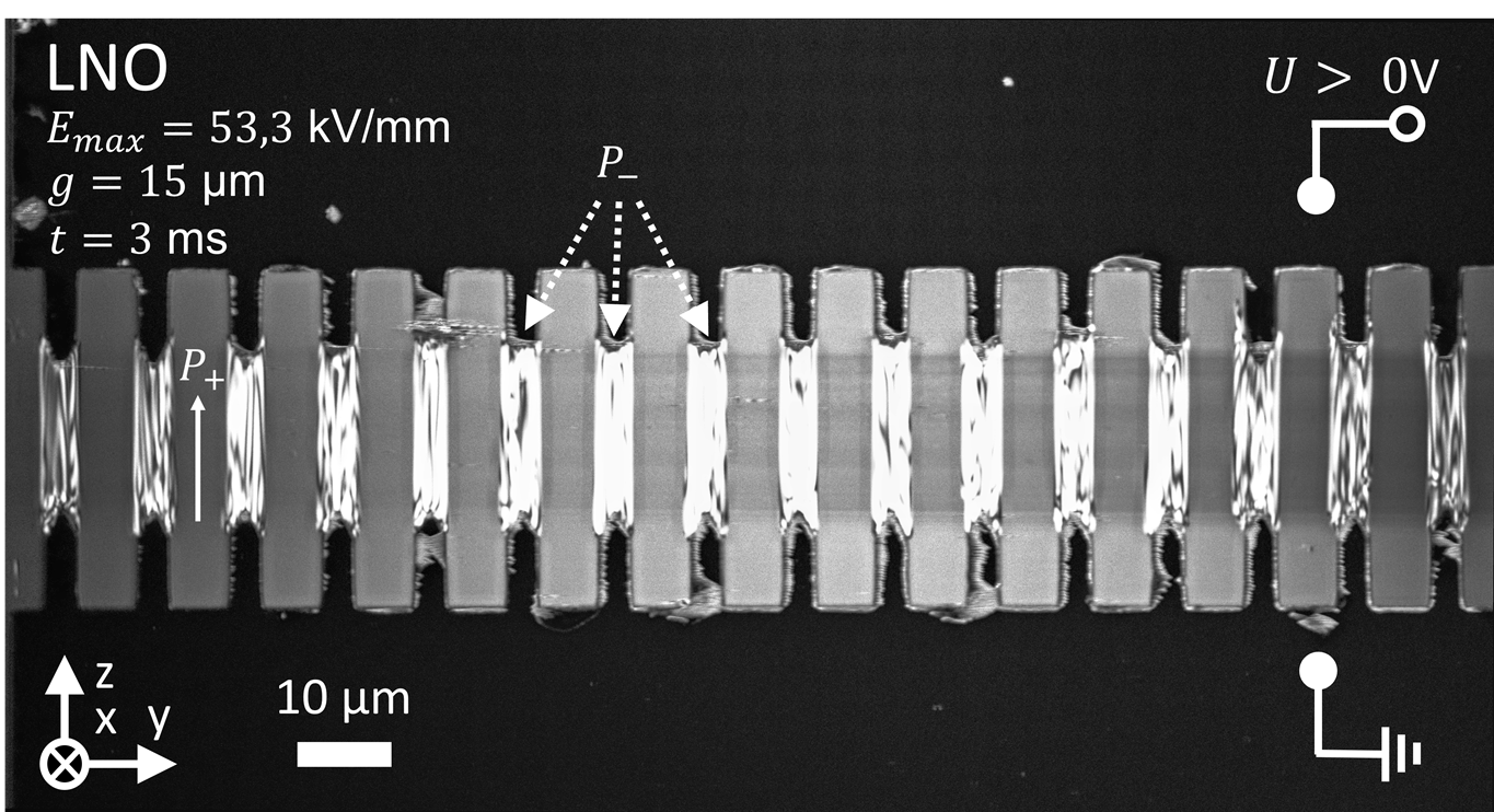
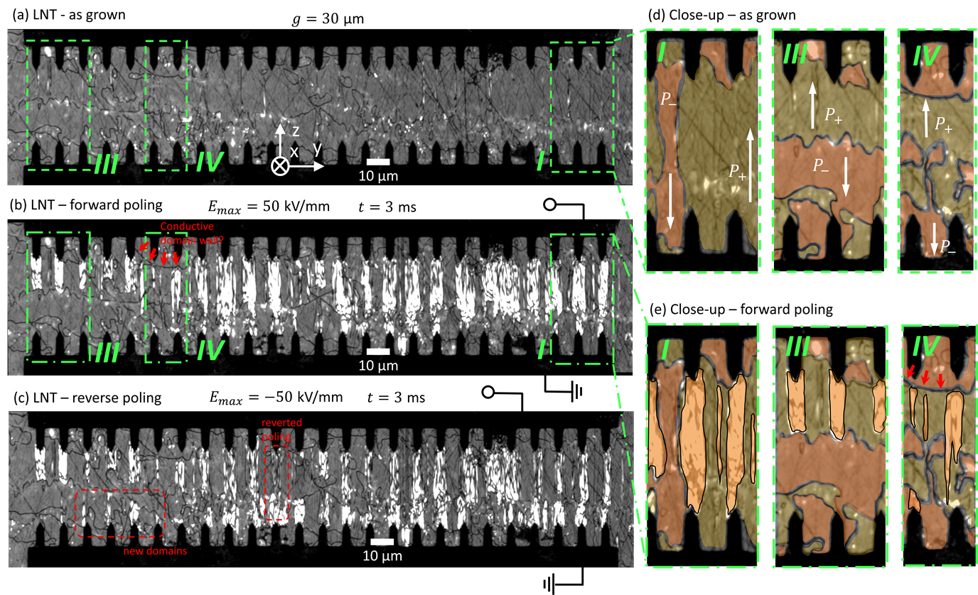
Figure 1(b) shows a sketch of a possible outcome of a poling experiment of a multi-domain crystal after applying a positive voltage to one of the electrodes. It is well established that domain nucleation in congruent crystals of the LNO-LTO material family only starts at the +z-direction of the crystal [24, 30, 25, 28, 23]. This means that inverted domains first nucleate at +z electrodes and grow towards the opposing electrode in the -z direction. Hence, four different cases in the relation of the as-grown domain pattern and the applied electric field can be distinguished [as highlighted in Fig. 1(b)]. In Case I the domain between two opposing electrode fingers is oriented completely opposed to the applied electric field. Here, inverted domains can readily nucleate at the +z electrode and grow over the full gap. Case II is the opposing case, where the as-grown domain between the electrodes is already aligned with the outer electric field. Here, nothing is expected to happen.
If the average size of the as-grown domains are in similar order of magnitude or smaller than the gap distance between the electrodes, the chance is high that there is at-least one head-to-head or tail-to-tail domain wall within the gap. Here, we can distinguish two more cases. In Case III, the domain directly under the positive electrode is of opposing nature (similar to Case I). In this case nucleation of new domains is possible directly at the +z electrode and inverted domains are expected to grow until these reach the tail-to-tail domain wall, where they merge with the domain of the same orientation.
Case IV is the most peculiar one. Here, the domain directly underneath the +z electrode, where the positive voltage is applied, is already aligned with the electric field (like in Case II). But somewhere within the gap one domain or more of opposing direction can be found, which may or may-not extent towards the -z electrode. If the electric field between two opposing electrodes is sufficiently large, any anti-parallel aligned domain within the gap, can invert, even if it does not intersect with the electrodes. However, aside from the necessary condition of the electric field being larger than the (effective) coercive field, the growth and nucleation of inverted domains also require the exchange of (screening) charges. For a single-domain, single crystal this is usually easily achieved, when the newly formed domains are in direct contact with an electrode (e.g. Case I or III). However, if the crystal is a good electrical insulator, which was shown for similarly grown lithium niobate tantalate at room temperature [19], it can be expected that poling in Case IV is largely inhibited, because no electrical contact and charge transport is possible. Nevertheless, nucleation and poling might still be possible, if the head-to-head domain walls, where the nucleation sites are expected, are conductive and have a connection to an electrode (example highlighted with red arrows). From previous works in lithium niobate and other ferroelectrics, it is well established that domain walls can be highly conductive in certain conditions, which particular applies to head-to-head domain walls [31, 32, 33, 22]. Therefore, if successful poling in LNTx in a Case IV is observed, this can be a first hint at domain wall conductivity in LNTx.
To analyze the poling results Second-Harmonic microscopy (SHM) images are taken before and after each time that electrical pulses are applied to an electrode pair. SHM is sensitive to ferroelectric domain structures and/or domain walls and is widely used to visualize domain structures [24, 34, 35, 36, 21, 37, 38, 33].
To test the experimental setup and electrode design and find initial poling parameters for the poling geometry, we performed poling experiments on a commercially-obtained, bulk-crystal of x-cut congruent LNO. Crucially, this also provides insights on the expected contrast from surface-near domains in SHM, which is important when interpreting SHM images from 3D domain structures [36, 23, 38]. In contrast to the LNTx crystal, the LNO sample is mono-domain before poling, i.e. the whole crystal is initially homogeneous with no domain walls present. Therefore, inverted domains can only grow when a positive voltage is applied to an electrode located on the +z end of a domain (compare Case I).
Figure 2 shows an SHM image of a poling experiment on a electrode with a gap of m and a length of several 100 m. The image was taken with the SHM focus placed surface-near, which results for the given wavelength and laser polarization in a homogeneous, strong SH signal from the surface [38, 37]. In SHM the metal electrodes always appear dark, because they do not possess any second-order nonlinearity. After application of a single electric pulse of 3 ms length with an electric field of 53.3 kV/mm within the gap, domain inversion between the fingers was observed. The applied electric field is more than two times larger then the value typically cited for z-cut congruent LNO ( 21 kV/mm) [39, 40]. However, this is not surprising, because such high fields were observed to be necessary when poling x-cut LNO in previous experiments as well [34, 26, 28, 24]. In standard z-cut poling inverted domains can directly grow vertical from the electrodes, while when using surface electrodes in x-cut poling a pronounced sideways growth into the depth of the crystal is required. Here, the electric field decays fast in the depth of the crystal necessitating much larger initial fields at the surface.
In our experiment in Fig. 2 the areas with domain inversion generate a stronger SHM signal compared to the surrounding bulk. This has been observed in SHM studies of surface-near domain inversion before [34, 26, 28, 24] and can be explained with constructive interference of the SHM signal generated in the surface-near inverted domain and the underlying bulk [23]. In these previous works it was observed that domains created in a similar configuration in congruent LNO typically penetrate 0.5 to 1 m within the gap, which yielded similar SHM images [26, 28, 41]. Further, it can be noticed that the newly poled domains also show an irregular, stripy pattern, which is indicative of spike domains which are not fully merged within the inverted regions. Again, similar was observed before when poling x-cut, congruent LNO with surface electrodes [26, 28, 24, 41].
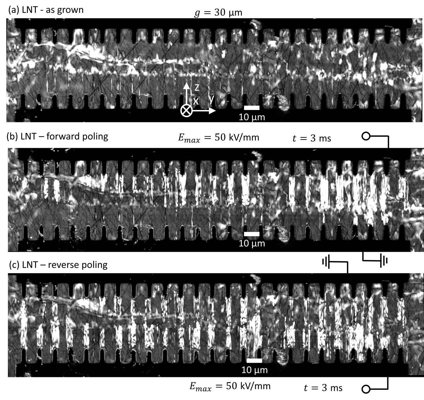
Figure 3 shows a result on the x-cut LNTx crystal along a 250 m long electrode with a gap of m. Here, panel (a) shows the SHM image before, (b) after application of a positive voltage to the top electrode (’forward poling’) and (c) application of the inverted voltage (’reverse poling’) are shown. Further, Figures (d) and (e) show close-ups of different regions from (a) and (b). In contrast, to the poled surface-near domains from Fig. 2 the as-grown domain walls in LNTx appear with a dark contrast. This is the typical contrast for domain walls, which are orthogonal to the surface and penetrate into the crystal [38, 37, 23, 35]. The domain pattern before poling is composed of many domains with typical width of 10 to 20 m along the z-axis. Here, most of the as-grown domain walls meander irregularly and randomly through the crystal forming a complex 3D domain pattern similar to previous observations [16]. In particular, these as-grown domains also form head-to-head and tail-to-tail sections, which normally are not favored in an uniaxial ferroelectric like LNO or LTO. Additionally, some brighter spots and areas can be seen, which indicate shallow, surface-near as-grown domains. Subfig. 3(d) shows a zoom-in into three areas with domain patterns of Case I, Case III, and Case IV, respectively. No domain pattern in accordance with Case II is found in this example. The suspected polarization is sketched in an overlay. The orientation of the polarization is reconstructed based on the poling and nucleation behavior observed after poling assuming only +z nucleation typical for LNO or LTO.
A positive poling pulse was applied with a duration of 3 ms and an electric field of 50 kV/mm similar to the values determined for bulk, congruent LNO. The results are shown in Fig. 3(b). Here, signatures of new surface-near domains can be seen for most electrode finger pairs. In more detail, it can be seen that the expected different behaviors for Cases I, III, and IV can be seen as highlighted in the close-ups in Figure 2(e). Here, as expected nucleation and growth is possible, when the original domain within the complete gap is oriented opposing the original domain (Cases I and Case III).
Case IV is the most peculiar. Here, it can be observed that nucleation at an as-grown head-to-head domain wall within the gap is possible in some areas, which is highlighted by red arrows in Fig. 3(e). However, as discussed below and presented in the supplement (e.g. Fig. S2) nucleation at head-to-head domain walls within the gap is not always possible. This immediately shows that reaching an electric field of the appropriate magnitude is a necessary condition, but not a sufficient condition to achieve domain inversion [42]. A potential mechanism allowing domain inversion in Case IV in Fig. 3 is an enhanced conductivity of the as-grown domain walls, which can facilitate the charge exchange required for domain reversal. For the as-grown domain wall highlighted by red arrows in Fig. 3(e) Case IV this might be given, because this head-to-head domain wall intercepts a neighboring electrode. In this regard, the random domain pattern of the as-grown crystals offer a distinct model system to study the role of conductivity for the growth an nucleation of domains. However, further investigations, e.g. by conductivity atomic force microscopy [22] is necessary to confirm the domain wall conductivity.
When applying a reversed voltage to the electrode pair domain growth can now start from the opposing electrodes, if the appropriate original domain orientation is given, as depicted in Fig. 3(c). Some back poling, i.e. a reversal of the previously poled domains, happens, but many poled domains from before (b) stay stable and are not influenced by a reverse poling pulse. This indicates the strongly pinned domains in the LNTx crystal.
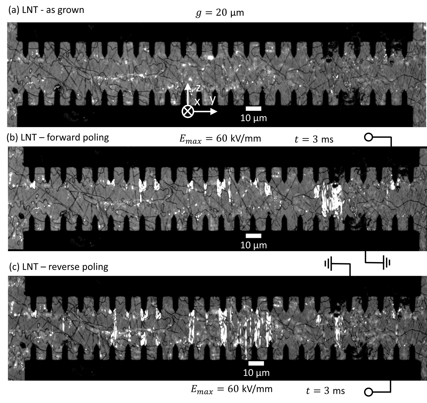
In the supplement, two more examples from the LNTx crystal are shown. Here, Fig. S1 shows a poling result on a electrode pair, which features a line defect running in the middle of the gap across most of the electrode length, which acts as a pinning site stopping domain growth from both sides. Due to the strong pinning by this defect structure, a periodic structure can be achieved after a positive pulse was applied to both electrodes with only minimal reverse poling.
In contrast, Fig. S2 depicts an electrode pair with a particular high density of as-grown domains with average distances of 5 m or less. Here, even though that fields up to 60 kV/mm are applied, only very few electrodes show signs of nucleation. If new domains nucleate, they immediately intercept a domain of the same orientation. Almost no additional nucleation of new domains within the gap similar to Case IV is observed. However, in this electrode pair, very few head-to-head domain walls, which could act as potential nucleation sites, appear to be connected with an electrode. This also supports the fact that the domain wall in Fig. 3 Case IV might be conductive and in contact with the electrodes to allow for nucleation, suggesting further study.
In conclusion, in this work we have demonstrated that surface-near periodic domain inversion over a poling gap of up to 30 m with a period of 10 m is possible within mixed crystals of lithium niobate tantalate. This lays the foundation to create nonlinear optical devices or tailor conductive domain walls within the whole LNTx material family. The poling of the as- grown domain structures provide an intricate model systems how both, defects and existing domain structures, can inhibit and pin domain growth on a larger scale within the lithium niobate tantalate material systems.
Acknowledgements.
The authors gratefully acknowledge financial support by the Deutsche Forschungsgemeinschaft (DFG) through collaborative research centers SFB-TRR142, project B07, (ID: 231447078) and CRC1415 (ID: 417590517), the Forschungsgruppe FOR5044 (ID: 426703838; http:www.For5044.de), the Würzburg-Dresden Cluster of Excellence ”ct.qmat” (EXC 2147), as well as by the Federal Ministry of Education and Research / Bundesministerium für Bildung und Forschung (Grant number 13N15975). We thank Dr. Steffen Ganschow from the IKZ Berlin for providing the crystal; and Thomas Gemming and Dina Bieberstein for assistance in dicing.
References
References
- Eckstein et al. [2011] A. Eckstein, B. Brecht, and C. Silberhorn, A quantum pulse gate based on spectrally engineered sum frequency generation, Opt. Express 19, 13770 (2011).
- Saravi et al. [2021] S. Saravi, T. Pertsch, and F. Setzpfandt, Lithium niobate on insulator: An emerging platform for integrated quantum photonics, Advanced Optical Materials 9, 2100789 (2021).
- Boes et al. [2023] A. Boes, L. Chang, C. Langrock, M. Yu, M. Zhang, Q. Lin, M. Lončar, M. Fejer, J. Bowers, and A. Mitchell, Lithium niobate photonics: Unlocking the electromagnetic spectrum, Science 379, eabj4396 (2023).
- Luo et al. [2019] K.-H. Luo, S. Brauner, C. Eigner, P. R. Sharapova, R. Ricken, T. Meier, H. Herrmann, and C. Silberhorn, Nonlinear integrated quantum electro-optic circuits, Science Advances 5, eaat1451 (2019).
- Stefszky et al. [2023] M. Stefszky, F. vom Bruch, M. Santandrea, R. Ricken, V. Quiring, C. Eigner, H. Herrmann, and C. Silberhorn, Lithium niobate waveguide squeezer with integrated cavity length stabilisation for network applications, Opt. Express 31, 34903 (2023).
- Harder et al. [2013] G. Harder, V. Ansari, B. Brecht, T. Dirmeier, C. Marquardt, and C. Silberhorn, An optimized photon pair source for quantum circuits, Opt. Express 21, 13975 (2013).
- Rusing et al. [2019] M. Rusing, P. O. Weigel, J. Zhao, and S. Mookherjea, Toward 3d integrated photonics including lithium niobate thin films: A bridge between electronics, radio frequency, and optical technology, IEEE Nanotechnology Magazine 13, 18 (2019).
- Weis and Gaylord [1985] R. S. Weis and T. K. Gaylord, Lithium niobate: Summary of physical properties and crystal structure, Applied Physics A 37, 191 (1985).
- Hum and Fejer [2007] D. S. Hum and M. M. Fejer, Quasi-phasematching, Comptes Rendus Physique 8, 180 (2007), recent advances in crystal optics.
- Byer [1997] R. L. Byer, Quasi-phasematched nonlinear interactions and devices, Journal of Nonlinear Optical Physics & Materials 06, 549 (1997).
- Zhao et al. [2023] J. Zhao, X. Li, T.-C. Hu, A. A. Sayem, H. Li, A. Tate, K. Kim, R. Kopf, P. Sanjari, M. Earnshaw, N. K. Fontaine, C. Wang, and A. Blanco-Redondo, Unveiling the origins of quasi-phase matching spectral imperfections in thin-film lithium niobate frequency doublers, APL Photonics 8, 126106 (2023).
- Bartasyte et al. [2019] A. Bartasyte, S. Margueron, A. M. Glazer, E. Simon, I. Gregora, S. Huband, and P. A. Thomas, Vibrational modes and overlap matrix of mixed crystals, Phys. Rev. B 99, 094306 (2019).
- Xue et al. [2000] D. Xue, K. Betzler, and H. Hesse, Dielectric properties of lithium niobate–tantalate crystals, Solid State Communications 115, 581 (2000).
- Sugii et al. [1976] K. Sugii, H. Koizumi, S. Miyazawa, and S. Kondo, Temperature variations of lattice parameters of lithium niobate, lithium tantalate and lithium-niobate-tantalate solid-solutions, Journal of Crystal Growth 33, 199 (1976).
- Bashir et al. [2023] U. Bashir, K. Böttcher, D. Klimm, S. Ganschow, F. Bernhardt, S. Sanna, M. Rüsing, L. M. Eng, and M. Bickermann, Solid solutions of lithium niobate and lithium tantalate: crystal growth and the ferroelectric transition, Ferroelectrics 613, 250 (2023).
- Roshchupkin et al. [2023] D. Roshchupkin, R. Fakhrtdinov, B. Redkin, V. Karandashev, V. Khvostikov, A. Mololkin, O. Siminko, and A. Zabelin, Growth of ferroelectric lithium niobate-tantalate crystals, Journal of Crystal Growth 621, 127377 (2023).
- Rüsing et al. [2016] M. Rüsing, S. Sanna, S. Neufeld, G. Berth, W. G. Schmidt, A. Zrenner, H. Yu, Y. Wang, and H. Zhang, Vibrational properties of lithium niobate tantalate mixed crystals, Phys. Rev. B 93, 184305 (2016).
- Wood et al. [2008] I. G. Wood, P. Daniels, R. H. Brown, and A. M. Glazer, Optical birefringence study of the ferroelectric phase transition in lithium niobate tantalate mixed crystals, Journal of Physics: Condensed Matter 20, 235237 (2008).
- Yakhnevych et al. [2023] U. Yakhnevych, C. Kofahl, S. Hurskyy, S. Ganschow, Y. Suhak, H. Schmidt, and H. Fritze, Charge transport and acoustic loss in lithium niobate-lithium tantalate solid solutions at temperatures up to 900c, Solid State Ionics 392, 116147 (2023).
- Koppitz et al. [2024] B. Koppitz, S. Ganschow, L. M. Eng, and M. Rüsing, Ferroelectric hysteresis measurement in the lithium niobate-lithium tantalate single-crystalline family: Prospects for lithium niobate tantalate, Phys. Stat. Sol. (a) accepted (2024).
- Kämpfe et al. [2014] T. Kämpfe, P. Reichenbach, M. Schröder, A. Haußmann, L. M. Eng, T. Woike, and E. Soergel, Optical three-dimensional profiling of charged domain walls in ferroelectrics by cherenkov second-harmonic generation, Phys. Rev. B 89, 035314 (2014).
- Singh et al. [2022] E. Singh, H. Beccard, Z. H. Amber, J. Ratzenberger, C. W. Hicks, M. Rüsing, and L. M. Eng, Tuning domain wall conductivity in bulk lithium niobate by uniaxial stress, Phys. Rev. B 106, 144103 (2022).
- Rüsing et al. [2019] M. Rüsing, J. Zhao, and S. Mookherjea, Second harmonic microscopy of poled x-cut thin film lithium niobate: Understanding the contrast mechanism, Journal of Applied Physics 126, 114105 (2019).
- Mackwitz et al. [2016] P. Mackwitz, M. Rüsing, G. Berth, A. Widhalm, K. Müller, and A. Zrenner, Periodic domain inversion in x-cut single-crystal lithium niobate thin film, Applied Physics Letters 108, 152902 (2016).
- Younesi et al. [2021] M. Younesi, R. Geiss, S. Rajaee, F. Setzpfandt, Y.-H. Chen, and T. Pertsch, Periodic poling with a micrometer-range period in thin-film lithium niobate on insulator, J. Opt. Soc. Am. B 38, 685 (2021).
- Gui et al. [2009] L. Gui, H. Hu, M. Garcia-Granda, and W. Sohler, Local periodic poling of ridges and ridge waveguides on x- and y-cut lithium niobate and its application for second harmonic generation, Opt. Express 17, 3923 (2009).
- Zhang et al. [2022] H. Zhang, Q. Li, H. Zhu, and H. Hu, Optimization of periodic poling of x-cut lithium niobate thin film, Optical Materials 131, 112562 (2022).
- Stanicki et al. [2020] B. J. Stanicki, M. Younesi, F. J. F. Löchner, H. Thakur, W.-K. Chang, R. Geiss, F. Setzpfandt, Y.-H. Chen, and T. Pertsch, Surface domain engineering in lithium niobate, OSA Continuum 3, 345 (2020).
- Wang et al. [2018] C. Wang, C. Langrock, A. Marandi, M. Jankowski, M. Zhang, B. Desiatov, M. M. Fejer, and M. Lončar, Ultrahigh-efficiency wavelength conversion in nanophotonic periodically poled lithium niobate waveguides, Optica 5, 1438 (2018).
- Sanna and Schmidt [2017] S. Sanna and W. G. Schmidt, Lithium niobate surfaces from a microscopic perspective, Journal of Physics: Condensed Matter 29, 413001 (2017).
- Beccard et al. [2022] H. Beccard, B. Kirbus, E. Beyreuther, M. Rüsing, P. Bednyakov, J. Hlinka, and L. M. Eng, Nanoscale Conductive Sheets in Ferroelectric BaTiO3: Large Hall Electron Mobilities at Head-to-Head Domain Walls, ACS Applied Nano Materials 5, 8717 (2022).
- Beccard et al. [2023] H. Beccard, E. Beyreuther, B. Kirbus, S. D. Seddon, M. Rüsing, and L. M. Eng, Hall mobilities and sheet carrier densities in a single lithium niobate conductive ferroelectric domain wall, Phys. Rev. Appl. 20, 064043 (2023).
- Kirbus et al. [2019] B. Kirbus, C. Godau, L. Wehmeier, H. Beccard, E. Beyreuther, A. Haußmann, and L. Eng, Real-time 3d imaging of nanoscale ferroelectric domain wall dynamics in lithium niobate single crystals under electric stimuli: Implications for domain-wall-based nanoelectronic devices, ACS Applied Nano Materials 2, 5787 (2019).
- Berth et al. [2007] G. Berth, V. Quiring, W. Sohler, and A. Zrenner, Depth-resolved analysis of ferroelectric domain structures in ti: PPLN waveguides by nonlinear confocal laser scanning microscopy, Ferroelectrics 352, 78 (2007).
- Spychala et al. [2020] K. J. Spychala, P. Mackwitz, M. Rüsing, A. Widhalm, G. Berth, C. Silberhorn, and A. Zrenner, Nonlinear focal mapping of ferroelectric domain walls in linbo3: Analysis of the shg microscopy contrast mechanism, J. Appl. Phys. 128, 234102 (2020).
- Cherifi-Hertel et al. [2021] S. Cherifi-Hertel, C. Voulot, U. Acevedo-Salas, Y. Zhang, O. Crégut, K. D. Dorkenoo, and R. Hertel, Shedding light on non-ising polar domain walls: Insight from second harmonic generation microscopy and polarimetry analysis, J. Appl. Phys. 129, 081101 (2021).
- Hegarty et al. [2022a] P. A. Hegarty, H. Beccard, L. M. Eng, and M. Rüsing, Turn all the lights off: Bright- and dark-field second-harmonic microscopy to select contrast mechanisms for ferroelectric domain walls, Journal of Applied Physics 131, 244102 (2022a).
- Hegarty et al. [2022b] P. A. Hegarty, L. M. Eng, and M. Rüsing, Tuning the Čerenkov second harmonic contrast from ferroelectric domain walls via anomalous dispersion, Journal of Applied Physics 132, 214102 (2022b).
- Kim et al. [2001] S. Kim, V. Gopalan, K. Kitamura, and Y. Furukawa, Domain reversal and nonstoichiometry in lithium tantalate, Journal of Applied Physics 90, 2949 (2001).
- Gopalan et al. [1998] V. Gopalan, T. E. Mitchell, Y. Furukawa, and K. Kitamura, The role of nonstoichiometry in 180° domain switching of LiNbO3 crystals, Applied Physics Letters 72, 1981 (1998).
- Berth et al. [2009] G. Berth, V. Wiedemeier, K.-P. Hüsch, L. Gui, H. Hu, W. Sohler, and A. Zrenner, Imaging of ferroelectric micro-domains in x-cut lithium niobate by confocal second harmonic microscopy, Ferroelectrics 389, 132 (2009).
- Sturman and Podivilov [2022] B. Sturman and E. Podivilov, Ferroelectric Domain Reversal: The Role of Domain Wall Conduction, JETP Letters 116, 246 (2022).
Supplement
