Resonant switching current detector based on underdamped Josephson junctions
Abstract
Current-biased Josephson junctions can act as detectors of electromagnetic radiation. At optimal conditions, their sensitivity is limited by fluctuations causing stochastic switching from the superconducting to the resistive state. This work provides a quantitative description of a stochastic switching current detector, based on an underdamped Josephson junction. It is shown that activation of a Josephson plasma resonance can greatly enhance the detector responsivity in proportion to the quality factor of the junction. The ways of tuning the detector for achieving optimal operation are discussed. For realistic parameters of Nb/AlOx/Nb tunnel junctions, the sensitivity and noise-equivalent power can reach values of (V/W) and (WHz-1/2), respectively. These outstanding characteristics facilitate both bolometric and single-photon detection in microwave and terahertz ranges.
Introduction
Sensitive, compact broad-range THz detectors are required for various applications, ranging from security and environmental monitoring, medical imaging, chemical analysis and fundamental research. Despite a large variety of available THz detectors (for review see e.g., [1, 2, 3, 4]), the search for a perfect sensor remains an active field of research. The key parameter, which requires further improvement is the sensor sensitivity, which is particularly important for passive THz detectors suitable for remote monitoring and imaging. The sensitivity can be greatly improved by cooling down to cryogenic temperatures, which both reduces the overall noise and removes the background black-body radiation. Ultra-sensitive cryogenic detectors based on semiconductors [5], graphene [6, 7, 8] and superconductors [9] have been demonstrated. Superconductors are particularly well suited for THz detection because characteristics energy scales (Josephson energy, superconducting gap, e.t.c.) are naturally placed in the THz range and could be easily tuned for achieving optimal operation.
A current-biased Josephson junction (JJ) demonstrates potential as a highly sensitive detector of electromagnetic waves, with the capability for single-photon resolution across a wide frequency range spanning from microwave (MW) to terahertz frequencies [10, 11, 12, 13, 14, 15, 16, 17, 18, 19, 20, 21, 22, 23, 24, 25]. The impacting electromagnetic wave induces a small alternating current, , in the JJ. If bias current is slightly below the critical current, , a very small may cause switching of the junction from the superconducting to the resistive state. An underdamped JJ will stay in the resistive state until the bias current is reduced to a retrapping current, [17, 20, 26, 27]. Such latching enables a long and large electric response to a small , thus enabling an easily measurable signal. The responsivity of such switching current detector (SCD) can be very high and is limited only by thermal and/or quantum fluctuations of phase [14, 16, 17, 18, 19, 20, 22, 25]. Therefore, stochastic effects associated with fluctuations, are essential for the analysis of SCD.
The operation frequency range of SCD is determined by the Josephson plasma frequency, and the characteristic frequency, , where and is the normal junction resistance. For low- superconductors it is sub-THz, but for high- it is in the THz range [23, 21, 28, 24]. Intrinsic Josephson junctions (IJJ’s) in layered Bi2Sr2CaCu2O8+δ (Bi-2212) cuprates [29] have the highest mV [30], facilitating operation in excess of 10 THz [21, 28]. The atomic scale of IJJ’s enables a strong coupling between junctions and allows integration of a large number of IJJ’s in a compact device [31, 32, 33, 34, 35, 36, 21, 24]. Arrays with many JJs can be used for cascade multiplication of the readout signal [37, 38, 39] and for achieving impedance matching with open space, which is required for the effective absorption of incoming radiation [40, 42, 41, 43].
In this work I present theoretical and numerical analysis of a stochastic SCD, based on an underdamped JJ. The key physical phenomenon that busts SCD performance is a resonant activation at the Josephson plasma frequency [45, 44, 15], which enhances the responsivity by the quality factor of the junction, . Various ways of tuning SCD for achieving optimal operation, are discussed. It is shown that the ultimate limit of sensitivity is determined by the phase diffusion phenomenon [46, 47, 27, 26]. Calculations based on realistic parameters for Nb/AlOx/Nb tunnel junctions show that the sensitivity and noise-equivalent power at K can reach values (V/W) and (WHz-1/2), respectively. These outstanding characteristics facilitate both bolometric and single-photon detection in MW and THz ranges. The paper is organized as follows. First we will recollect basic concepts on fluctuation-induced statistics in the absence of radiation and on MW response in the absence of fluctuations, followed by consideration of a general problem of MW response in the presence of fluctuations. We will start with the case of non-resonant escape at low frequencies and then consider resonant activation at . In the end we will discuss limitations and ultimate performance.
Results
We consider an underdamped JJ with a quality factor . Here , is the zero-bias plasma frequency, is the fluctuation-free critical current, is the flux quantum, is capacitance and is the low-bias (subgap) quasiparticle resistance, which for tunnel JJs is much larger than the high-bias . Photon detection by overdamped JJ with has been studied earlier [10, 11, 12] (for an overview see e.g. Ch. 11.5 in Ref. [48]). The sensitivity (V/W) of such the detector is proportional to the differential resistance of the current-voltage (-) characteristics at the bias point, . However, this simple description is inapplicable for us because underdamped JJs have an abrupt switching from the superconducting to the resistive state. For tunnel JJs the voltage jumps from zero to a large sum-gap value, . In this case and the device operation can be described only statistically in terms of switching probabilities.
Dynamics of a JJ is equivalent to motion of a particle in a tilted washboard potential [48], , as sketched in Fig. 1 (a). Here is the Josephson phase difference, is the Josephson energy and . The washboard has bias-dependent parameters: the barrier height, , the eigenfrequency , and the quality factor, . Below I will show calculations for the typical experimental situation of ac-bias, , at Hz, K, and parameters corresponding to Nb/AlOx/Nb tunnel junctions with mV and mV [49].
Switching statistics without external radiation
Fluctuations cause premature escape out of the well at a switching current . The escape rate in the absence of radiation can be written as [50, 51, 52].
| (1) |
For underdamped JJs excited by thermal fluctuations, the prefactor can be written as [53], . The effect of quantum fluctuations at can be easily taken into account by introducing an effective escape temperature [50]. The probability density for switching in the bias interval is
| (2) |
where is the bias ramp rate and
| (3) |
is the total probability of switching upon ramping up to current . Eqs. (2) and (3) form a recurrent equation, which can be easily solved numerically.
Microwave response without fluctuations
In the absence of fluctuations the MW response of JJ has been studied in connection with the analysis of Shapiro steps. Electromagnetic waves induce both voltage and current oscillations in the junction. Since JJ is essentially non-linear, a self-consistent treatment of both voltage and current components is a difficult task. To simplify the analysis, voltage- or current-source approximations are employed [48].
The simplest is the voltage-source approximation. It postulates the harmonic MW voltage, and yields an explicit expression for the fluctuation-free critical current [48]:
| (4) |
where is the zero-order Bessel function. Unfortunately, this simple expression is not applicable for the analysis of SCD in the most interesting frequency range . Eq. (4) works only at frequencies well above , but at low frequencies it gives a qualitatively incorrect prediction of increasing (diverging) responsivity with decreasing , which is opposite to reality (see Fig. 2(e) below).
The current-source approximation postulates a harmonic MW current, . This is a more complex approach, which allows only numerical solution. However, it provides a physically correct results at low frequencies. In agreement with experiment, it predicts a linear reduction of vs. at (see ch. 11.3 in Ref. [48]). This has a clear physical explanation. At low frequencies the junction dynamics is quasi stationary. Therefore, bias and MW currents simply add up. The switching occurs when the total current exceeds , which yields,
| (5) |
At frequencies well above , current- and voltage-source solutions are in a qualitative agreement with each other [48], although the connection between , and the absorbed MW power, , remains uncertain. To couple them we need to introduce a MW impedance , so that and
| (6) |
where the MW resistance, . This resistance has nothing to do with . For example, in the current-source model, vertical shaking of the potential by leads also to a horizontal motion of the particle, as indicated by the black dashed line in Fig. 1 (a). The associated MW voltage is connected to via the impedance of the nonlinear Josephson induction of the junction. In reality, represents the total MW impedance of the device, including electrodes, which should be designed and act as antennas for effective catching of MW [41].
Microwave response with fluctuations
In the presence of MW, the total current is oscillating,
| (7) |
This leads to shaking of the washboard potential, as shown in Fig. 1 (a), which enhances the escape rate,
| (8) |
by some gain factor . The most prominent enhancement occurs when coincides with the eigenfrequency , leading to excitation of a plasma resonance.
Non-resonant escape at
In the low-frequency limit, the dynamics is quasi-stationary. Therefore, barrier characteristics and are well defined at every time instance and the escape rate is obtained from Eq. (1) with a given time-dependent , Eq. (7). Thus the modified escape rate is obtained by time-averaging over the MW period, ,
| (9) |
Switching probabilities are obtained by substituting it in Eqs. (2) and (3), taking into account the actual time dependent bias ramp rate in Eq. (7). Note, that the escape gain in this limit is frequency independent.
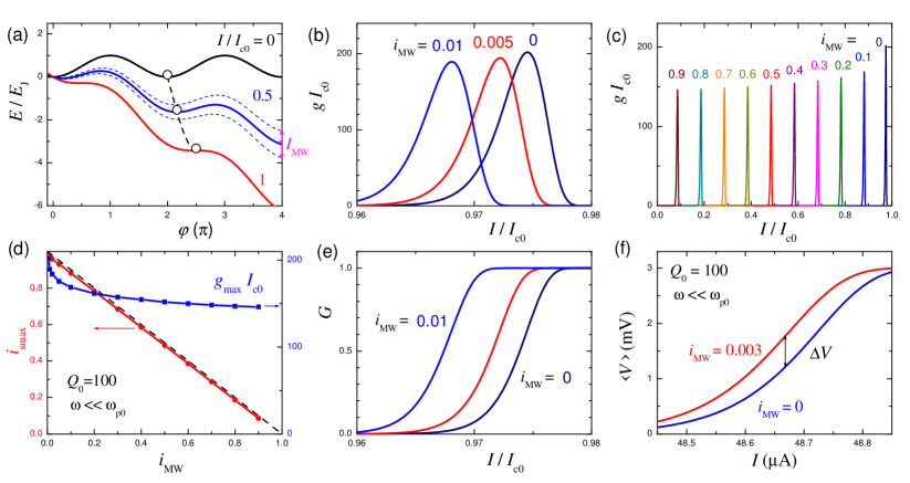
Figs. 1 (b) and (c) show thus calculated probability densities for different MW amplitudes, , for a JJ with A. They corresponds to experimentally measurable switching current histograms, . It is seen that the MW excitation leads to a shift of histograms with successive reduction of the most probable switching current . Fig. 2 (d) represents the MW-dependence of (red squares, left axis). The black dashed line shows the fluctuation free according to Eq. (5). Blue circles (right axis) represent the maximum probability density . It exhibits a rapid decline at small and then saturates at larger . As will be shown below, the rapid decline ensures a non-diverging responsivity at , see Fig. 3 (a). Fig. 1 (e) shows switching probabilities for the same as in Fig. 1 (b). Since tunnel junctions switch to the bias-independent gap voltage, represent the time-average dc-voltage, . Note that although varies gradually with , the switching remains abrupt at each measurement.
Fig. 1 (f) clarifies the operation principle of the SCD. Here time-average - characteristics, , are shown without MW (blue) and with a small (red). The voltage response, , is equal to the vertical shift of the curves. At small , it is proportional to the shift and the slope of the step-like ,
| (10) |
Therefore, maximum sensitivity is achieved at the steepest part in the middle of the step .
Resonant activation at
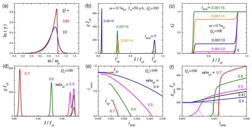
Josephson plasma resonance occurs when [45, 44, 15]. Since the amplitude of forced oscillations is proportional to , resonant activation greatly enhances the escape rate in underdamped junctions with . In Ref. [44] a fitting function was suggested for the resonant gain factor :
| (11) | |||
| (12) | |||
| (13) |
(in these expressions I used explicit values for parameters , in Eq. (6.5) from Ref. [44], as suggested by the authors, and , as follows from Fig. 19 from Ref. [44]).
Figure 2 (a) shows resonant escape gain factors for and 100, calculated from Eqs. (11-13). They resemble response functions of a driven oscillator, but have a sharp exponential cutoff at [45]. The resonant escape is easily analyzed by substituting Eqs. (11-13) in Eq. (8) and subsequently in Eqs. (2) and (3).
Fig. 2 (b) shows calculated switching histograms for , A, , K for several MW amplitudes, . The plasma resonance is manifested by a bifurcation at some threshold MW amplitude, leading to splitting of histograms [44, 15, 20]. A new plasma peak emerges at a switching current, , lower than that in the absence of MW, . Fig. 2 (c) shows the two-step switching probabilities in the bifurcation region.
The plasma peak corresponds to the resonant condition , yielding,
| (14) |
Fig. 2 (d) shows split-histograms at different MW frequencies. It can be seen that moves upwards with reducing , in accord with Eq. (14). Figs. 2 (e) and (f) show MW amplitude dependencies of (e) peak currents and (d) heights, , for several MW frequencies. From Fig. 2 (e) it is seen that decay approximately parabolically with . The dependency becomes stronger with increasing , which is in contrast to Eq. (4), but in line with Eq. (14).
The bifurcation region can be extremely narrow: in Fig. 2 (c) it starts at and finishes at 0.00115. Its width, , is two orders of magnitude narrower than that in the absence of MW, as shown in Fig. 1 (b). The extremely narrow bifurcation region indicates an extraordinary sensitivity to MW. However, the problem for detector application is in the presence of a threshold , below which the response is practically zero. This follows from the independence of sub-threshold and on , as shown by open symbols in Figs. 2 (e) and (f). From Figs. 2 (d-f) it can be seen that the threshold is reduced with reducing frequency and disappears when the two peaks merge, . At this point the plasma resonance occurs within the accessible bias range for . For the chosen parameters in Fig. 2, this occurs at , indicated by the black line in Fig. 2 (f). Inverting Eq. (14), we can see that SCD has optimal sensitivity at
| (15) |
At higher frequencies the threshold appears. At lower frequencies switching occurs before reaching the resonant conditions.
Discussion
A good sensor should have a large sensitivity, and a low noise-equivalent-power (NEP). However, equally important, it should have a high absorption efficiency, i.e., the ratio of absorbed to impacting MW power. A junction alone can not absorb the MW power because its size is much smaller that the electromagnetic wavelength in free space, , [41]. Therefore, achieving a high efficiency requires implementation of impedance-matching MW antennas [41, 40, 42]. In what follows I shall assume in Eq. (6), typical for well-matched MW devices.
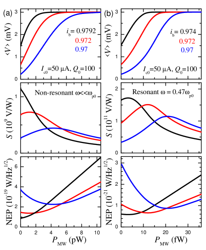
Figures 3 summarizes performances of (a) non-resonant SCD at low frequencies and (b) resonant SCD at the optimal frequency, . They are based on simulations from Figs. 1 and 2, respectively. Top panels show time-average voltage versus for three bias amplitudes, , close to . Middle panels represent sensitivities. Largest sensitivities at low are achieved for black curves at bias current corresponding to the middle of the steps . With increasing the response saturates at . This occurs when the shift of exceeds the width of the histogram , as for the blue curve at from Fig. 1 (e). By reducing the bias current below the optimal point it is possible to extend the dynamic range at the expense of lower sensitivity. Bottom panel show NEP. Calculation of NEP requires estimation of the voltage noise in the measurement setup. It is in the range of few nV/Hz1/2 for conventional dc-measurements, but could be greatly reduced by lock-in measurements [54]. The lock-in technique is particularly suitable for statistical measurements of SCD response over many bias periods [21]. Below I will assume nV/Hz1/2, easily accessible with lock-in readout.
Although the behavior of non-resonant and resonant SCD’s from Figs. 3 (a) and (b) is qualitatively similar, there are important differences. First of all, the resonant SCD has a significantly higher sensitivity as a consequence of resonant activation. Another important difference is the frequency and -dependencies. The response of non-resonant SCD is frequency independent within the range of applicability, . It is also almost independent of , which appears only in the prefactor of Eq. (1). For the resonant SCD the situation is completely different, as illustrated in Figure 4.
Fig. 4 (a) shows frequency dependence of the time-average voltage at different bias amplitudes for a small . Junction parameters are the same as in Fig. 2. The response shows a sharp peak at , which corresponds to the plasma resonance in this bias range. The shape of the peak reflects the resonant gain factor, shown by the red line in Fig. 2 (a). The maximum response is obtained at , corresponding to the middle of the switching step, (red curve). The optimal sensitivity at this bias is shown by black lines in Fig. 3 (b). Thus, the resonant SCD has a very strong frequency dependence.
The ultimate sensitivity of SCD
The sensitivity and NEP, shown in Fig. 3 (b) are remarkably good, in line or even better than the most sensitive photon detectors reported so far [2, 6, 5, 7, 8]. However, this is not the ultimate limit of a resonant SCD. These calculations are made for fairly modest junction parameters and there are several ways to improve the sensitivity. Firstly, the responsivity is determined by the relative MW current, . Therefore, the sensitivity is increasing with decreasing . This can be done by reducing the junction area or by suppression of the critical current with magnetic field, . Secondly, the resonant gain is increasing with the quality factor, as seen from Fig. 2 (a). Thus, optimization of sensitivity requires proper tuning of junction parameters.
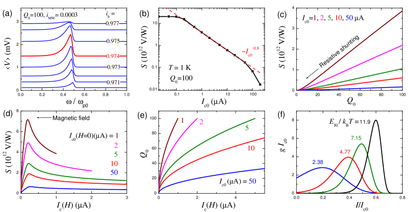
Reducing the junction area proportionally reduces , while keeping and unchanged. In Fig. 4 (b) we show a log-log plot of the optimal sensitivity for junctions with different area and at a fixed . The red line indicates that scales as , before it saturates at (V/W), corresponding to an astonishing value of (W/Hz1/2). This is the ultimate limit for and K, but it could be further increased by increasing and decreasing .
The quality factor can be tuned by resistive shunting of the junction. In this case the stays constant, but is reduced. Fig. 4 (c) shows optimal sensitivities versus the quality factor for junctions with several fixed . It is seen that increases approximately linear with at , as expected for forced plasma oscillations.
Finally, it is possible to in-situ tune junction parameters by changing temperature or applying magnetic field [50]. Figs. 4 (d) and (e) illustrate the effect of magnetic field. Here we consider junctions with different areas having the same , but different at . With application of magnetic field is suppressed and is reduced , as shown in Fig. 4 (e). This drives the sensitivity in opposite directions and leads to appearance of maxima in , as shown in Fig. 4 (d).
Yet the ultimate sensitivity is limited by another phenomenon - entrance in the phase-diffusion state [46, 47, 26, 27]. With reducing , the Josephson energy is reducing proportionally. When becomes comparable with , the particle is no longer stationary in the washboard, but can diffuse in the potential even without a tilt at . Fig. 4 (f) shows switching histograms without MW for , 0.2, 0.3 and 0.5 A, corresponding to 2.38, 4.22, 7.15 and 11.9, respectively. It is seen that becomes significantly larger than zero at A (red curve) for K. From Figs. 4 (b) and (d) it can be seen that the maxima of sensitivity are reached at the same current A, irrespective of . As seen from Fig. 4 (f), entering in the phase-diffusion state broadens the switching histograms, which deteriorates the sensor performance. Nevertheless, the sensor may still work even in the phase diffusion state. Moreover, sharpening of switching histograms may occur in moderately damped junctions [47, 26, 27], but the analysis of operation at the edge of phase-diffusion requires proper analysis of the retrapping process, which is beyond the scope of this work. The phase diffusion can be reduced by lowering the temperature, with the ultimate limit set by the crossover temperature to macroscopic quantum tunneling (MQT) , which is typically few tens of mK [50, 51, 52, 14]. Alternatively, the sensitivity can be improved by increasing the quality factor, e.g. by means of an additional capacitive shunting of the junction [26]. Cascade amplification of the readout voltage using arrays of coupled JJs can also strongly enhance the ultimate sensitivity [39].
Limitations
As seen from Fig. 4 (b), for realistic parameters of Nb/AlOx/Nb tunnel junctions with , the limits of sensitivity and noise-equivalent power at K reach outstanding values of (V/W) and (WHz-1/2). However, it comes at a certain expense.
Firstly, although the achievable sensitivity would be more than sufficient for single photon resolution in the MW range, however SCD at the maximal sensitivity has dark count rate and, therefore, does not work as a single photon detector. It is possible to reduce the dark count rate by reducing bias, but this comes at the expense of reduced sensitivity, as shown in Fig. 3. Yet, the sensitivity is so high that a certain reduction may be tolerated in order to enable a robust single photon detection.
Secondly, at the optimal sensitivity SCD is quite slow. Because of a large dark-count rate, the response signal can be obtained only by collecting a large statistical ensemble, which takes time. On a positive side, lock-in measurement can be performed over many bias periods to reduce noise [21, 54]. In the sub-optimal regime with deterministic photon counting, a single switching event is sufficient and, therefore, it could be fast.
Thirdly, the resonant SCD is a narrow-band detector with the maximum sensitivity at , as shown in 2 (a). For given experimental settings, optimal sensitivity is achieved at a frequency given by Eq. (15). However, a JJ is easily tunable. The plasma frequency can be varied from the maximum value to zero by applying a small magnetic field, as shown in Fig. 4 (d).
Beyond the resonant region a JJ may still have a good and broad-band non-resonant response, as demonstrated in Fig. 3 (a) for the case . For higher frequencies, , the response is caused by a simple shift of the switching histograms according to Eq. (4). Expanding the latter for small amplitudes, , and using Eq. (10), we obtain for the maximum sensitivity.
| (16) |
Taking into account that for the case of Fig. 1 (b), we obtain (V/W) at GHz. This is comparable to the low-frequency non-resonant sensitivity, shown in Fig. 3 (a). However, the high-frequency non-resonant response, Eq. (16), decays quadratically with increasing frequency.
To conclude, I described the operation of a stochastic switching current detector of electromagnetic radiation, based on an underdamped Josephson junction. The key physical phenomenon that busts SCD performance is a resonant activation at a Josephson plasma frequency. The plasma resonance enhances the detector responsivity by the quality factor of the junction. The ways of tuning the detector for achieving optimal operation are discussed. For realistic parameters of Nb/AlOx/Nb tunnel junctions with , the sensitivity and noise-equivalent power at K can reach limiting values of (V/W) and (WHz-1/2), respectively. These outstanding characteristics facilitate both bolometric and single-photon detection in microwave and terahertz ranges.
Acknowledgements
The work was supported by the Science for Peace and Security Program, grant G5796. Stimulating discussions with R. Hovhannisyan and R. Cattaneo are gratefully acknowledged.
References
- [1] M. Zhang and J.T.W. Yeow, Nanotechnology-Based Terahertz Biological Sensing. IEEE Nanotechn. Mag. 10, 30 (2016).
- [2] R. A. Lewis, A review of terahertz detectors. J. Phys. D: Appl. Phys. 52, 433001 (2019).
- [3] S. R. Kasjoo, M. B. Mohd Mokhar, N. F. Zakaria and N. J. Juhari, A brief overview of detectors used for terahertz imaging systems. AIP Conf. Proc. 2203, 020020 (2020).
- [4] M. D. Eisaman, J. Fan, A. Migdall, and S. V. Polyakov. Invited Review Article: Single-photon sources and detectors. Rev. Sci. Instrum. 82, 071101 (2011).
- [5] S. Komiyama, O. Astafiev, V. Antonov, T. Kutsuwa, and H. Hirai, A single-photon detector in the far-infrared range. Nature 403, 405 (2000).
- [6] G. Auton, D. B. But, J. Zhang, E. Hill, D. Coquillat, C. Consejo, P. Nouvel, W. Knap, L. Varani, F. Teppe, J. Torres, and A. Song, Terahertz Detection and Imaging Using Graphene Ballistic Rectifiers. Nano Lett. 17, 7015 (2017).
- [7] G.-H. Lee, D. K. Efetov, W. Jung, L. Ranzani, E. D. Walsh, T. A. Ohki, T. Taniguchi, K. Watanabe, P. Kim, D. Englund, K. C. Fong. Graphene-based Josephson junction microwave bolometer. Nature 586, 42 (2020).
- [8] E. D. Walsh, W. Jung, G.-H. Lee, D. K. Efetov, B.-I. Wu, K.-F. Huang, T. A. Ohki, T. Taniguchi, K. Watanabe9, P. Kim, D. Englund, K. C. Fong, Josephson junction infrared single-photon detector. Science 372, 409–412 (2021).
- [9] J. A. Lau, V. B. Verma, D. Schwarzer, and A. M. Wodtke, Superconducting single-photon detectors in the mid-infrared for physical chemistry and spectroscopy. Chem. Soc. Rev. 52, 921 (2023).
- [10] C. C. Grimes, P. L. Richards, S. Shapiro. Josephson‐Effect Far‐Infrared Detector. J. Appl. Phys. 39, 3905–3912 (1968).
- [11] H. Kanter, F. L. Vernon, Jr. High‐Frequency Response of Josephson Point Contacts. J. Appl. Phys. 43, 3174–3183 (1972).
- [12] A.N. Vystavkin, V.N. Gubankov, L.S. Kuzmin, K.K. Likharev, V.V. Migulin, V.K. Semenov. S-c-S junctions as nonlinear elements of microwave receiving devices. Rev. de Physique Appl. 9, 79-109 (1974).
- [13] J. R. Tucker, M. J. Feldman. Quantum detection at millimeter wavelengths. Rev. Mod. Phys. 57, 1055 (1985).
- [14] I. A. Devyatov, L. S. Kuzmin, K. K. Likharev, V. V. Migulin, A. B. Zorin. Quantum‐statistical theory of microwave detection using superconducting tunnel junctions. J. Appl. Phys. 60, 1808-1828 (1986).
- [15] N. Grønbech-Jensen, M. G. Castellano, F. Chiarello, M. Cirillo, C. Cosmelli, L.V. Filippenko, R. Russo, and G. Torrioli. Microwave-Induced Thermal Escape in Josephson Junctions. Phys. Rev. Lett. 93, 107002 (2004).
- [16] A. Poudel, R. McDermott, and M. G. Vavilov. Quantum efficiency of a microwave photon detector based on a current-biased Josephson junction. Phys. Rev. B 86, 174506 (2012).
- [17] G. Oelsner, L. S. Revin; E. Il’ichev, A. L. Pankratov, H.-G. Meyer, L. Grönberg, J. Hassel, and L. S. Kuzmin. Underdamped Josephson junction as a switching current detector. Appl. Phys. Lett. 103, 142605 (2013).
- [18] C. K. Andersen, and K. Mølmer. Effective description of tunneling in a time-dependent potential with applications to voltage switching in Josephson junctions. Phys. Rev. A 87, 052119 (2013).
- [19] K. Inomata, Z. Lin, K. Koshino, W. D. Oliver, J.-S. Tsai, T. Yamamoto, and Y. Nakamura. Single microwave-photon detector using an artificial -type three-level system. Nature Commun. 7, 12303 (2016).
- [20] G. Oelsner, C. K. Andersen, M. Rehák, M. Schmelz, S. Anders, M. Grajcar, U. Hübner, K. Mølmer, and E. Il’ichev. Detection of Weak Microwave Fields with an Underdamped Josephson Junction. Phys. Rev. Appl. 7, 014012 (2017).
- [21] E. A. Borodianskyi and V. M. Krasnov, Josephson emission with frequency span 1-11 THz from small Bi2Sr2CaCu2O8+δ mesa structures, Nat. Commun. 8, 1742 (2017).
- [22] L. S. Revin, A. L. Pankratov, A. V. Gordeeva, A. A. Yablokov, I. V. Rakut, V. O. Zbrozhek, and L. S. Kuzmin. Microwave photon detection by an Al Josephson junction. Beilstein J. Nanotechnol. 11, 960–965 (2020).
- [23] V. V. Pavlovskiy, I. I. Gundareva, O. Y. Volkov, Y. Y. Divin. Wideband detection of electromagnetic signals by high- Josephson junctions with comparable Josephson and thermal energies. Appl. Phys. Lett. 116, 082601 (2020).
- [24] R. Cattaneo, E. A. Borodianskyi, A. A. Kalenyuk, and V. M. Krasnov, Superconducting Terahertz Sources with 12% Power Efficiency. Phys. Rev. Appl. 16, L061001 (2021).
- [25] F. Chiarello, et al., Investigation of Resonant Activation in a Josephson Junction for Axion Search With Microwave Single Photon Detection. IEEE Trans. Appl. Supercond. 32, 1100305 (2022).
- [26] V. M. Krasnov, T. Bauch, S. Intiso, E. Hürfeld, T. Akazaki, H. Takayanagi, and P. Delsing, Collapse of Thermal Activation in Moderately Damped Josephson Junctions. Phys. Rev. Lett. 95, 157002 (2005).
- [27] V. M. Krasnov, T. Golod, T. Bauch and P. Delsing, Anticorrelation between temperature and fluctuations of the switching current in moderately damped Josephson junctions. Phys. Rev. B 76, 224517 (2007).
- [28] S. O. Katterwe, H. Motzkau, A. Rydh, and V. M. Krasnov. Coherent generation of phonon-polaritons in Bi2Sr2CaCu2O8+x intrinsic Josephson junctions. Phys. Rev. B 83, 100510(R) (2011).
- [29] R. Kleiner and P. Müller, Intrinsic Josephson effects in high- superconductors. Phys. Rev. B 49, 1327 (1994).
- [30] V. M. Krasnov. Interlayer tunneling spectroscopy of Bi2Sr2CaCu2O8+δ: A look from inside on the doping phase diagram of high- superconductors. Phys. Rev. B 65, 140504(R) (2002).
- [31] L. Ozyuzer, A. E. Koshelev, C. Kurter, N. Gopalsami, Q. Li, M. Tachiki, K. Kadowaki, T. Yamamoto, H. Minami, H. Yamaguchi, T. Tachiki, K. E. Gray, W.-K. Kwok, and U. Welp, Emission of Coherent THz Radiation from Superconductors. Science 318, 1291 (2007).
- [32] T. M. Benseman, K. E. Gray, A. E. Koshelev, W.-K. Kwok, U. Welp, H. Minami, K. Kadowaki, and T. Yamamoto, Powerful terahertz emission from Bi2Sr2CaCu2O8+δ mesa arrays. Appl. Phys. Lett. 103, 022602 (2013).
- [33] T. Kashiwagi, T. Yamamoto, H. Minami, M. Tsujimoto, R. Yoshizaki, K. Delfanazari, T. Kitamura, C. Watanabe, K. Nakade, T. Yasui, K. Asanuma, Y. Saiwai, Y. Shibano, T. Enomoto, H. Kubo, K. Sakamoto, T. Katsuragawa, B. Marković, J. Mirković, R. A. Klemm, and K. Kadowaki, Efficient Fabrication of Intrinsic-Josephson-Junction Terahertz Oscillators with Greatly Reduced Self-Heating Effects. Phys. Rev. Appl. 4, 054018 (2015).
- [34] H. Zhang, R. Wieland, W. Chen, O. Kizilaslan, S. Ishida, C. Han, W. Tian, Z. Xu, Z. Qi, T. Qing, Y. Lv, X. Zhou, N. Kinev, A. B. Ermakov, E. Dorsch, M. Ziegele, D. Koelle, H. Eisaki, Y. Yoshida, V. P. Koshelets, R. Kleiner, H. Wang, and P. Wu, Resonant Cavity Modes in Bi2Sr2CaCu2O8+x Intrinsic Josephson Junction Stacks, Phys. Rev. Appl. 11, 044004 (2019).
- [35] Y. Ono, H. Minami, G. Kuwano, T. Kashiwagi, M. Tsujimoto, K. Kadowaki, R. A. Klemm. Superconducting Emitter Powered at 1.5 Terahertz by an External Resonator. Phys. Rev. Appl. 13, 064026 (2020).
- [36] M. Tsujimoto, S. Fujita, G. Kuwano, K. Maeda, A. Elarabi, J. Hawecker, J. Tignon, J. Mangeney, S. S. Dhillon, I. Kakeya. Mutually Synchronized Macroscopic Josephson Oscillations Demonstrated by Polarization Analysis of Superconducting Terahertz Emitters. Phys. Rev. Appl. 13, 051001(R) (2020).
- [37] J. C. LeFebvre, E. Cho, H. Li, K. Pratt, and S. A. Cybart, Series arrays of planar long Josephson junctions for high dynamic range magnetic flux detection. AIP Adv. 9, 105215 (2019).
- [38] S. Yu. Grebenchuk, R. Cattaneo, and V. M. Krasnov. Nonlocal Long-Range Synchronization of Planar Josephson-Junction Arrays. Phys. Rev. Appl. 17, 064032 (2022).
- [39] R. Cattaneo, A. E. Efimov, K. I. Shiianov, O. Kieler, and V. M. Krasnov, Cascade switching current detectors based on arrays of Josephson junctions. preprint.
- [40] M. M. Krasnov, N. D. Novikova, R. Cattaneo, A. A. Kalenyuk and V. M. Krasnov, Design aspects of Bi2Sr2CaCu2O8+δ THz sources: optimization of thermal and radiative properties. Beilstein J. Nanotechnol. 12, 1392 (2021).
- [41] V. M. Krasnov, A distributed active patch antenna model of a Josephson oscillator. Beilstein J. Nanotechnol. 14, 151 (2023).
- [42] C.A. Balanis, Antenna Theory: Analysis and Design, 3rd ed.; John Wiley & Sons, Inc., Publ.: Hoboken, New Jersey, 2005.
- [43] V. M. Krasnov, Coherent flux-flow emission from stacked Josephson junctions: Nonlocal radiative boundary conditions and the role of geometrical resonances. Phys. Rev. B 82, 134524 (2010).
- [44] M. H. Devoret, D. Esteve, J. M. Martinis, A. Cleland, and J. Clarke, Resonant activation of a Brownian particle out of a potential well: Microwave-enhanced escape from the zero-voltage state of a Josephson junction. Phys. Rev. B 36, 58 (1987).
- [45] A. I. Larkin and Yu. N. Ovchinnikov, Resonance Reduction of the Lifetime of the Metastable State of Tunnel Junctions. J. Low Temp. Phys. 63, 317 (1986).
- [46] R. L. Kautz and J. M. Martinis, Noise-affected I-V curves in small hysteretic Josephson junctions. Phys. Rev. B 42, 9903 (1990).
- [47] J. M. Kivioja, T. E. Nieminen, J. Claudon, O. Buisson, F. W. J. Hekking, and J. P. Pekola, Observation of Transition from Escape Dynamics to Underdamped Phase Diffusion in a Josephson Junction. Phys. Rev. Lett. 94, 247002 (2005).
- [48] A. Barone and G. Paterno, Physics and Applications of the Josephson Effect (John Wiley & Sons, 1982),
- [49] N. V. Kinev, K. I. Rudakov, L. V. Filippenko, A. M. Baryshev, and V. P. Koshelets, IEEE Trans. Terahertz Sci. Technol. 9, 557–564 (2019).
- [50] J. M. Martinis, M. H. Devoret, and J. Clarke, Experimental tests for the quantum behavior of a macroscopic degree of freedom: The phase difference across a Josephson junction. Phys. Rev. B 35, 4682 (1987).
- [51] H. Grabert, P. Olschowski, and U. Weiss, Quantum decay rates for dissipative systems at finite temperatures. Phys. Rev. B 36, 1931 (1987).
- [52] J. M. Martinis and H. Grabert, Thermal enhancement of macroscopic quantum tunneling: Derivation from noise theory. Phys. Rev. B 38, 2371 (1988).
- [53] M. Büttiker and R. Landauer, Traversal Time for Tunneling. Phys. Rev. Lett. 49, 1739 (1982).
- [54] R. A. Hovhannisyan, O. M. Kapran, T. Golod and V. M. Krasnov, Accurate Determination of the Josephson Critical Current by Lock-In Measurements. Nanomaterials 11, 2058 (2021).