.
Understanding the Interlayer Coupling in
1T/1H-NbSe2 Hetero-Bilayers
Abstract
The properties of 2D materials are strongly influenced by their substrate, leading to a variety of ”proximity effects” like screening, charge transfer, and hybridization. Surprisingly, there is a dearth of theoretical studies on these effects. Particularly, previous theoretical research on the Star of David (SOD) structure in 1T-NbSe2 has focused on single-layer configurations or stacking with the same 1T phase without any real substrate. Here, we depart from these approaches and explore how these proximity effects shape the electronic and magnetic properties of the 1T-NbSe2 phase when it is grown on the metallic 1H-NbSe2 substrate. Using Density Functional Calculations, we establish a common framework to define the key characteristics of both free-standning 1T-NbSe2 and 1H-NbSe2. We then identify the optimal stacking arrangement for these two layers, revealing a transfer from the 1T to the 1H phase and a reorganization of charge within each layer. Our findings indicate that the magnetic moment of the SOD structure is still robust; however, is diminished due to a reduction in the on-site Coulomb interaction of the Hubbard bands. Additionally, the interlayer coupling induces metallicity in the 1T phase and increases the decoupling of the lower Hubbard band from the valence band.
I Introduction
In recent years, two-dimensional (2D) van der Waals (vdW) materials, particularly transition metal dichalcogenides (TMDs), have captured the attention of the scientific community[1, 2]. These materials, heralded for their versatile applications in optoelectronic and spintronic technologies, offer a unique playground for material engineering and device fabrication[3]. Among TMDs, NbSe2 is a prominent example, showcasing a spectrum of electronic phases such as charge density wave (CDW), superconductivity, and variable electronic structures in its different phases like single layers (SL) of the 1H and 1T phases.[4, 5, 6, 7, 8]. The 1T phase of NbSe2, distinct from the 1H phase in terms of symmetry and electronic properties, adds an extra layer of complexity and potential to these materials, paving the way for tailoring the overall properties of the system through phase engineering. While the 1H phase is a metal, that at low temperatures ( = 7.2K for bulk and Tc = 3.2K for the monolayer [9, 10, 4, 11, 12]) develops superconductivity, the 1T was first identified as a Mott insulator[13], recently instead it has been characterized as a Charge Transfer Insulator (CT)[8].
The interplay between the 1H and 1T phases in hetero-layers of NbSe2 enriches its physical properties, allowing for the manipulation of electronic and spin states in novel ways. This ability to tailor the characteristics of TMDs by controlling their phase composition opens new avenues for customized material properties, particularly in the context of proximity effects in heterostructures and their applications in advanced technologies [14].
More recently, magnetic impurities have been deposited on clean surfaces of NbSe2, resulting in the appearance of Yu-Shiba-Rusinov (YSR) bound states in the superconducting gap[15]. This could be linked to the creation of a topological phase and Majorana bound states. The experimental exploration of the vertically stacked 1T and 1H NbSe2 layers (hereafter referred to as 1T/1H) has unveiled intriguing phenomena that occur at the interface of these two phases. When the 1T phase is combined with the 1H phase, distinct and noteworthy effects have been observed, such as the emergence of Yu-Shiba-Rusinov (YSR) bound states and Kondo resonances within the superconducting gap[8]. These effects highlight the complex and unique interactions at the 1T/1H interface, showcasing how the combination of different phases can lead to new physical behaviors.
These experimental results suggest a significant modification of electronic and magnetic properties at the interface. This modification indicates an underlying influence that could be akin to a proximity effect[16], where the presence of one phase impacts the properties of the adjacent phase. These findings are pivotal in understanding the coupled dynamics of the 1T and 1H phases and offer valuable insights into the potential mechanisms driving their interaction. This experimental backdrop forms an important context for our theoretical study.
From the theoretical point of view and within the framework of calculations based on the Density Functional Theory (DFT), the simultaneous description of monolayers in 1H and 1T phases of is a great challenge due to the different physical characteristics that each of them presents. Consequently, different approximations are utilized in their computational treatment to address this complexity and enhance the overall accuracy of the theoretical framework [17, 6, 18, 8].
In this theoretical work, we intend to simultaneously capture the main features of both phases from DFT calculations finding a common set of parameters such as lattice parameter and effective on-site Coulomb interaction (Ueff), that correctly describe both phases. Then we shift our focus towards exploring the interactions at the interlayer interface. This exploration is crucial for understanding how the distinct properties of each phase influence each other when combined in a heterostructure. We investigate the nuances of interlayer coupling, particularly how it affects the electronic and magnetic properties of the combined system. This part of our work aims to provide a deeper insight into the synergistic effects at play between the 1H and 1T phases, shedding light on the potential of these interactions to induce novel phenomena in NbSe2 heterostructures.
II Methods
Spin polarized DFT calculations were performed with the VASP code [19, 20, 21, 22, 23, 24] within the slab-supercell approach and using the projector augmented-wave (PAW) method [23]. Wave functions were expanded using a plane wave basis set with an energy cut-off of 500 eV. We used the PBE functional [25] to treat the exchange-correlation energy. We added the missing van der Waals interactions using the Tkatchenko-Scheffler scheme [26]. The strongly-correlated correction is considered with the DFT+U approach [27] to deal with the Nb d-electrons. In this study, we investigated the influence of varying Ueff values for Nb(d) atoms on the lattice constant, electronic properties, and magnetic properties of isolated 1T and 1H monolayers (see Supporting Information). Furthermore, we used linear response theory [28] to estimate an optimal value for both monolayers. Overall, this approach allowed us to analyze the interplay between electronic structure, magnetic behavior, and lattice parameters, providing valuable insights into the properties of these materials. The isolated monolayers of 1H and 1T were studied using 11 and unit cells. Test calculations for the 33 CDW of the 1H phase revealed that our primarily conclusions remain unchanged, even when considering a 11 unit cell. The 33 CDW in NbSe2 is weak and does not significantly alter the band structure or DOS. For the heterobilayer 1T/1H, a unit cell was used. It is worth mentioning that incorporating a commensurate unit cell for the CDW of both 1T and 1H layers would necessitate an unfeasible large unit cell. The 4p64d45s1 states of Nb atoms and the 4s24p4 states of Se atoms are treated as valence states. For ionic relaxation, we used a 13131 and 331 k-grids for 11 and , respectively. For the PDOS, we used a 1001001 and 18181 k-grids for 11 and , respectively.
To analyze the charge transfer process, we employed the Bader scheme [29] to calculate the charge in the 1T/1H, 1T and 1H optimal structures. In order to gain further insights, we also computed the difference between the charge densities of the entire 1T/1H model and the separated 1T and 1H layers, denoted as . Here, , , and refer to the charge densities of the whole 1T/1H system, the 1T layer, and the 1H layer, respectively. To obtain and , we removed the 1H monolayer and the 1T layers from the entire system respectively, while keeping the remaining atomic structures unchanged.
III Results and Discussion
III.1 Single-layer (SL) of 1T and 1H NbSe2
Single layers of 1H-NbSe2 consist of hexagonal arrangements of Nb atoms enveloped within a trigonal prismatic Se atom environment (see Figure 1). Prior theoretical investigations have highlighted various atomic structures that are compatible with the 33 CDW distortions, and these alternatives exist within a narrow energy range of approximately 3 meV per formula unit [6]. This intriguing observation suggests a coexistence of these structures. Moreover, the deviations in atomic positions from the ideal 11 arrangement are relatively minor [6]. These findings collectively illuminate the complex interplay between structural modifications and electronic behaviours within the intricate landscape of 1H-NbSe2. When it comes to the role of magnetism in 1H-NbSe2, the exact nature of this phase is not clear [17, 6, 30].
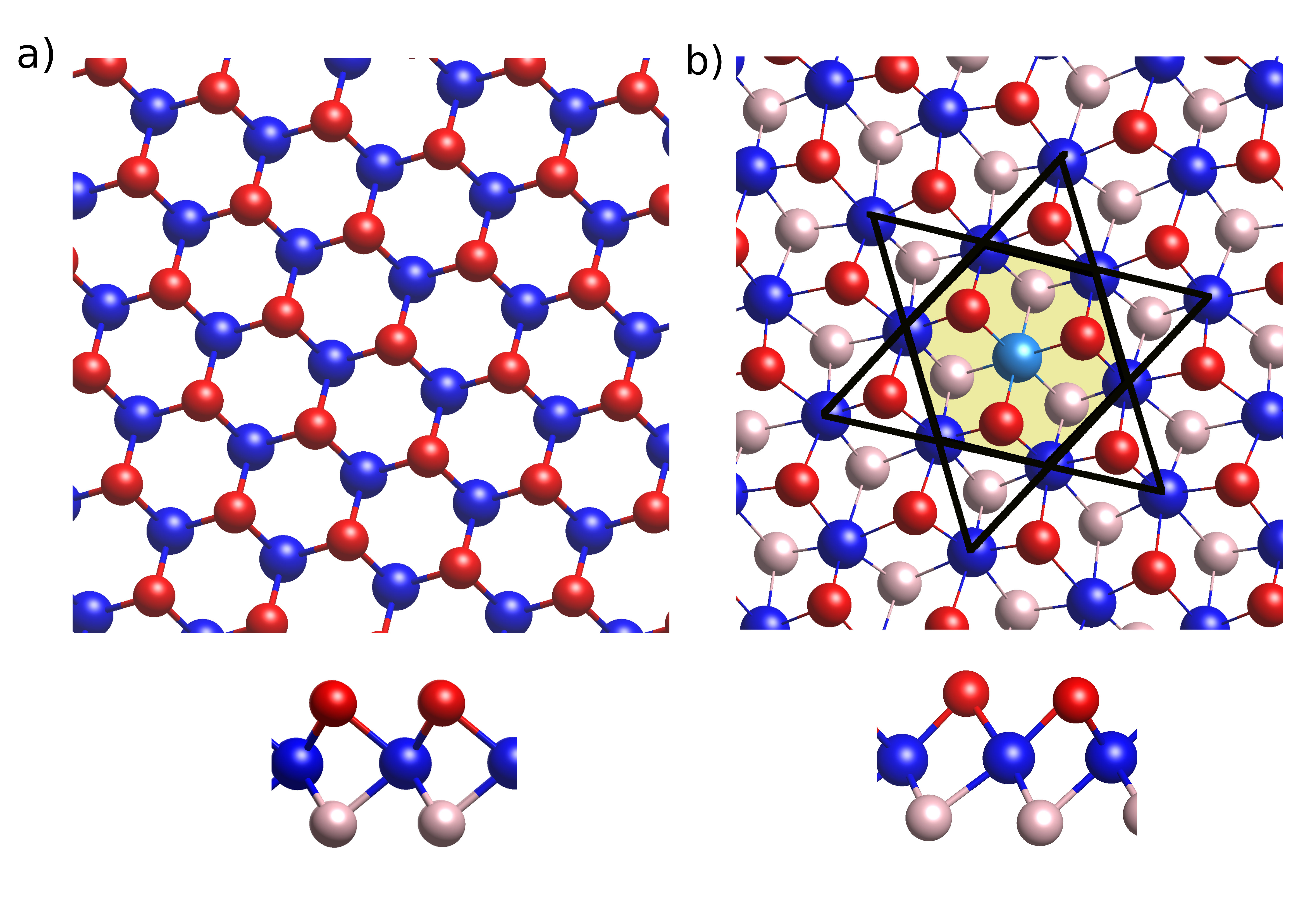
Regarding the 1T-NbSe2 phase, mono- and few-layers are, so far, experimentally accessible using molecular beam epitaxy [13, 8, 31, 32, 33]. The single-layer (SL) 1T-NbSe2 phase is characterized by a distinctive star-of-David (SOD) CDW pattern with a periodicity [13]. Within this CDW pattern, each SOD comprises twelve outer Nb atoms that undergo contraction toward a central Nb atom. Additionally, six Se atoms are positioned in the upper plane and six in the lower plane of each SOD, as visually depicted in Figure 1. In contrast to the 1H polytype, in the 1T phase, each Nb atom achieves octahedral coordination with its neighboring Se atoms. 1T-NbSe2 is proposed as a Charge Transfer insulator [8], in which the Valence Band (VB), mainly composed of the Se pz states, appreciably hybridizes with the Lower Hubbard Band (LHB) [34, 31].
In light of our ultimate objective, which centers on the comprehensive investigation of the physical characteristics exhibited by bilayer configurations composed of 1T and 1H stacked structures, it becomes paramount to establish a singular computational approach capable of encapsulating their salient attributes. Of particular significance is the determination of a unique lattice constant and the appropriate choice of the parameter for the treatment of Nb(4d) electrons. These parameters are pivotal not only in rendering an accurate representation of the metallic and insulating characteristics intrinsic to 1H and 1T single layers but also in elucidating their magnetic properties.
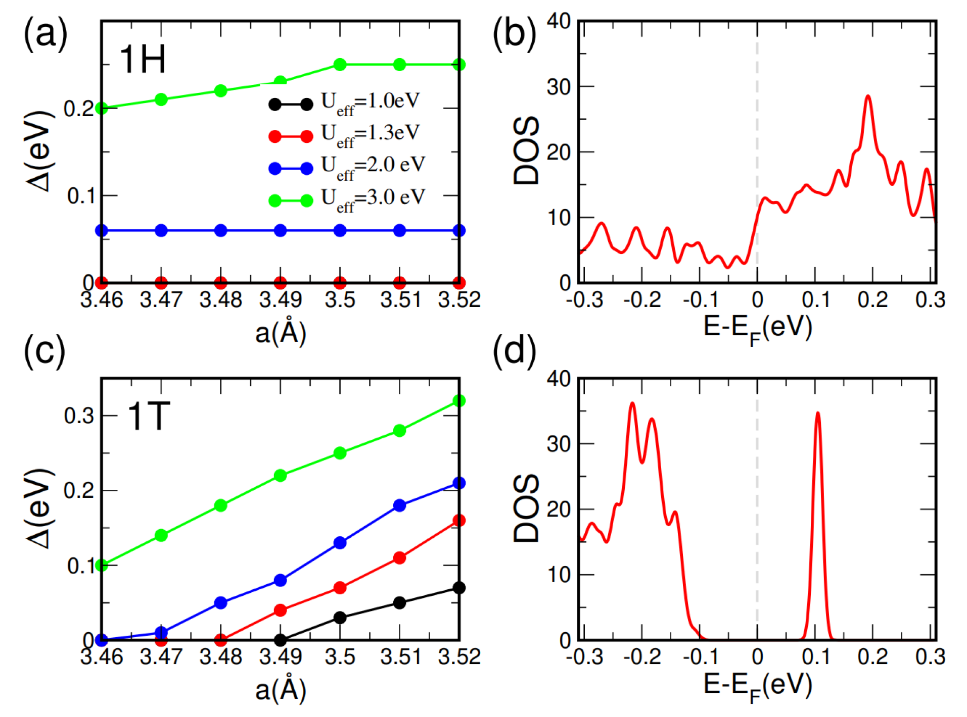
For the 1H single layer (SL), the variation of the band gap, denoted as , with respect to the lattice constant is depicted in Figure 2(a) for different values of . As expected, for high enough values of the Hubbard parameter, 2 eV, the system becomes an insulator. Additionally, due to the presence of an odd number of electrons within the unit cell, the total magnetic moment is MT = 1 when the system becomes an insulator. An intriguing observation to note is that, for a fixed value of , the strain applied to the SL does not exert a pronounced influence on the band gap. All in all, the metal-to-insulator transition triggered by strong electron-electron correlations imposes constraints on the permissible range of values that we can select to accurately model the established electronic characteristics of the 1H SL. In particular, when considering 1.3 eV, it is noteworthy that the SL exhibits a consistently metallic behaviour across the entire range of lattice parameters examined. While the presented results correspond to a 11 structural model, test calculations considering geometries based on the 33 CDW exhibit similar trends, further enhancing the validation of our findings.
In the context of the 1T SL, we apply a methodology similar to that used for the 1H counterpart. However, we investigate a unit cell configuration, which is a distinctive feature associated with the SOD.
In Figure 2(c), we illustrate a pronounced dependence of on both lattice parameters and the interaction parameter. This dependence also translates to the magnetic properties (see Figure S2 in the SI). For instance, for small enough values of both parameters, the known insulator state and the magnetic characteristics of the 1T phase (SOD) are lost. This outcome aligns with previous research findings that have underscored a strong correlation between the charge transfer gap and the structural distortion linked to the SOD [35]. Particularly, the authors have emphasized the potential of applying mechanical strain as a promising strategy for the precise adjustment and fine-tuning of the charge transfer gap in this material [35]. It is noteworthy to highlight that, within the context of the 1T SL, an increase in strain results in a corresponding augmentation of the magnetic moment and this phenomenon may be attributed to the enhanced super-exchange interaction, as suggested by Liu et al. [36].
Putting together the information gathered so far on 1H and 1T SLs, it is clear that our nuanced and balanced approach can effectively capture and describe the collective physical properties of both SL configurations. In particular, we have identified that setting the effective Hubbard interaction parameter, , to 1.3 eV, and the lattice constant to 3.52 Å, successfully reproduces the main characteristics of the density of states (DOS) (see 2(b-d)) and magnetic characteristics of both the experimental 1T and 1H phases. This choice preserves the metallic and insulating properties characteristic of each phase, respectively. For the 1T-SL, our calculations indicate a band gap of 0.15 eV, in good agreement with the experimental gap (i.e 0.15 eV) found by Liu et al [8]. Furthermore, the SOD exhibits behavior akin to that of a spin-1/2 system, with the central Nb atom () and its nearest neighbor Nb atom () displaying magnetic moments of 0.43 and 0.36 (in total), respectively.
It is worth noting that the selected lattice constant exhibits minimal dispersion, with a variation of less than 1% compared to the optimal values, being for 1H and for 1T. Furthermore, these chosen lattice constants align well with experimental measurements (i.e. 34814 pm and 34311 pm for 1H and 1T respectively) [37].
Additionally, we implemented linear response theory [28] and obtained for both phases an eV, very close to our choice of . This validates both the chosen value and the use of a single one for both phases.
III.2 Heterogeneous 1T/1H NbSe2 bilayer
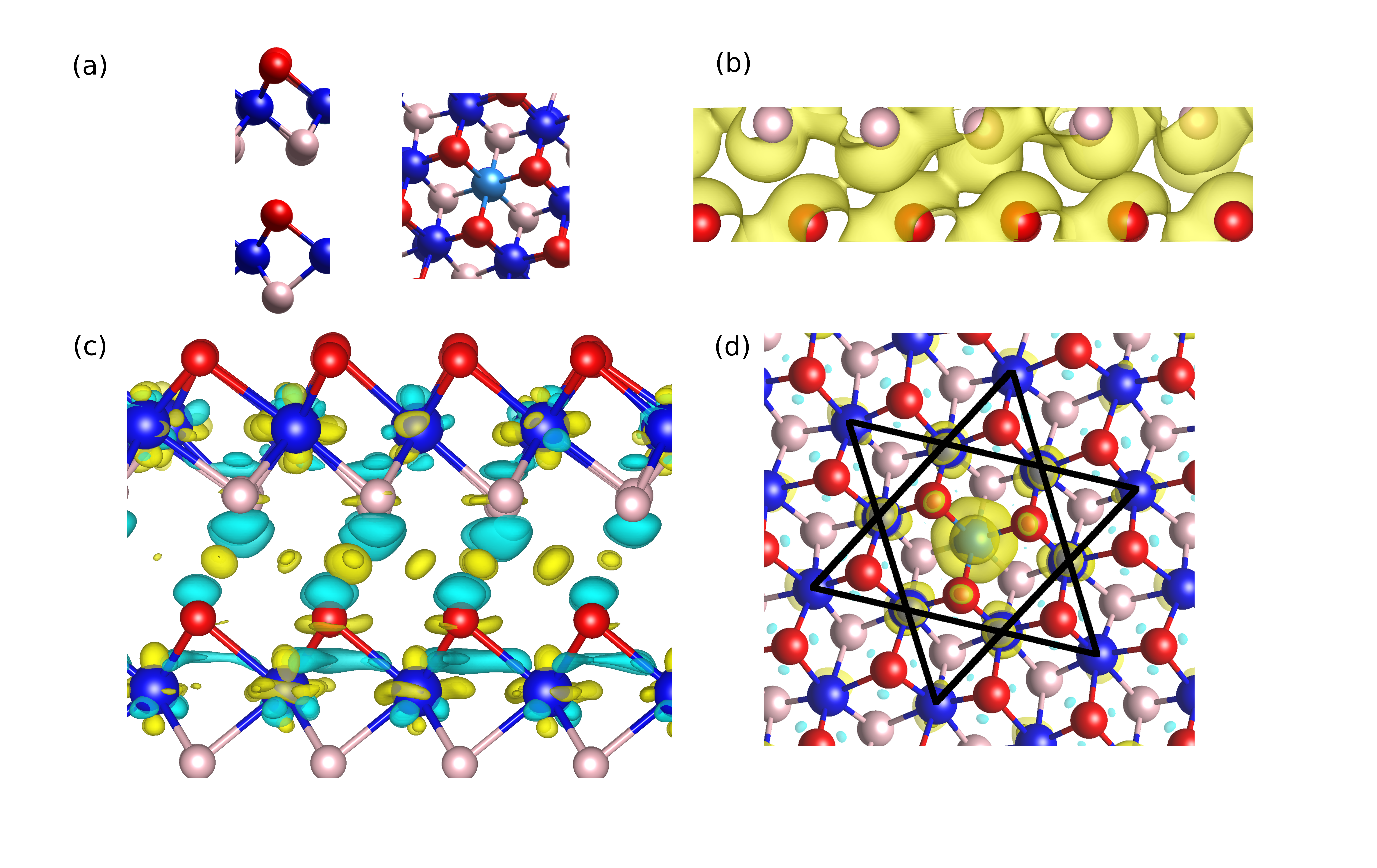
To determine the optimal arrangement of the 1T-NbSe2 on 1H-NbSe2 substrate, we explored different stacking configurations (Figure S3 in the SI). There are six high symmetry adsorption sites where the 1T monolayer can stack on top of the 1H monolayer [38, 39]. Figure 3(a) shows the lowest energy stacking geometry. Here, the Nb atoms in the 1T and 1H SLs lie on top of each other, and the interfacial Se atoms in the bottom layer, denoted as B1T within the 1T arrangement, align precisely with the hollow sites corresponding to the interfacial Se atoms in the top layer, designated as T1H within the 1H structure. This geometric arrangement gives rise to a hexagonal pattern when viewed from the top. The interlayer distance between the Nb atoms in 1T and 1H layers is dint= 6.08 Å consistent with the distance between planes in bulk 2H- (i.e. 6.2 0.1 Å) [40] while the distance between Se in the B1T and T1H layers is 2.8 Å. The cohesive energy between the layers is -4.47 eV, with the van der Waals (vdW) contribution being -5.13 eV.
The hexagonal stacking among Se atoms in the interface greatly enhances the interfacial wavefunction overlap among them. Each Se atom within the B1T layer engages in hybridized interactions with its closest neighbors in the T1H layer, as visually depicted in Figure 3(b). This bonding interaction results in the emergence of interlayer bonds that exhibit characteristics akin to ”covalent-like quasi-bonds.”[41] Such interlayer bonding behavior has been observed in other bilayer systems as well, as referenced in prior works [41]. These results serve as a distinctive hallmark of the interlayer interactions occurring between the 1T and 1H layers.
The interlayer interaction is thoroughly elucidated through a comprehensive analysis of the charge transfer process between the 1T and 1H arrangements, as visualized in Figure 3(c) and summarized in Table 1. This investigation reveals a charge transfer and reorganization when comparing the monolayers to the newly constructed bilayer structure. In particular, the central Nbc atom within the 1T phase, and to a somewhat lesser extent, the neighboring Nb1 atoms, exhibit a marginal decrease in charge, with charge variations per atom quantifying at less than 0.01 . The external Nb atoms of the SOD accumulate a marginal charge of 0.01 per atom. All in all, the net change in the overall charge of the Nb layer within the 1T phase amounts to a mere increment of 0.01 . Notably, the lower Se atoms within the 1T phase experience a charge loss approximately five times more significant than their upper counterparts within the same phase, resulting in a net charge reduction of 0.18 within the Se layers of the 1T phase. Consequently, a charge transfer of 0.17 is observed, flowing from the 1T phase to the 1H phase. This is in line with our expectations, as it is consistent with the reduced work function of the 1T phase, eV, relative to the 1H phase eV. Within the 1H layer, a distinct redistribution of charge is also observed. The Nb layer increases its charge by 0.27 , while there is a slight charge depletion (0.10 ) in the Se layers. It is important to highlight that the charge transfer from the 1T phase to the 1H layer is significantly reduced when compared to the TaS2 system, as previously documented in Crippa et al. [42], and this variation in the charge transfer process may lead to other distinct behaviors and outcomes.
All in all, the charge transfer and reorganization processes, as outlined earlier, result in the concentration of charge at the interface between the 1T and 1H layers, with a notable emphasis on the vicinity of the Se atoms of the B1T and T1H layers (see Figure3(c)). This observation aligns with the presence of interfacial states, visually exemplified in Figure 3(b). Additionally, when the 1T and 1H layers come into close proximity, it leads to a reduction in the magnetic moment of the SOD structure, as indicated in Table 1. Similar to the single-layer (SL) case, the magnetic moment of the SOD (see Figure 3(d)), primarily originates from the Nb(dz2) states of Nbc and Nb1 atoms. However, it is noteworthy that the total magnetic moment of these states decreases from 0.72 in the 1T-SL configuration to 0.43 in the 1T-BL configuration.
| Species | (Nb) (e-) | (Se) (e-) | (Nb) () | (Se) () |
| 1T | 0.014 (tot.) | -0.180 (tot.) | -0.180 (Nbc) | 0 (av.) |
| 1H | 0.273 (total) | -0.107 (total) | -0.102 (av.) | 0 (av.) |
The electronic hybridization of interfacial Se atoms and the charge transfer processes among the layers are pivotal factors that significantly influence the electronic structures of the entire system, contrasting with the properties of their isolated components.
In the SL-1T, as depicted in Figure 4(a), the valence band and the Lower Hubbard Band (LHB) are known to undergo hybridization, resulting in a broad peak [43], which, in our specific study, is centered at -0.22 eV. This hybridization arises from the significant overlap of the Se pz states within the valence band with the LHB [43]. The complex interplay of these electronic states poses a substantial challenge when it comes to precisely determining the position of the LHB. In contrast, the Upper Hubbard Band (UHB) in the 1T-SL exhibits a well-defined, narrow peak, which, in our investigation, is centered at 0.11 eV.
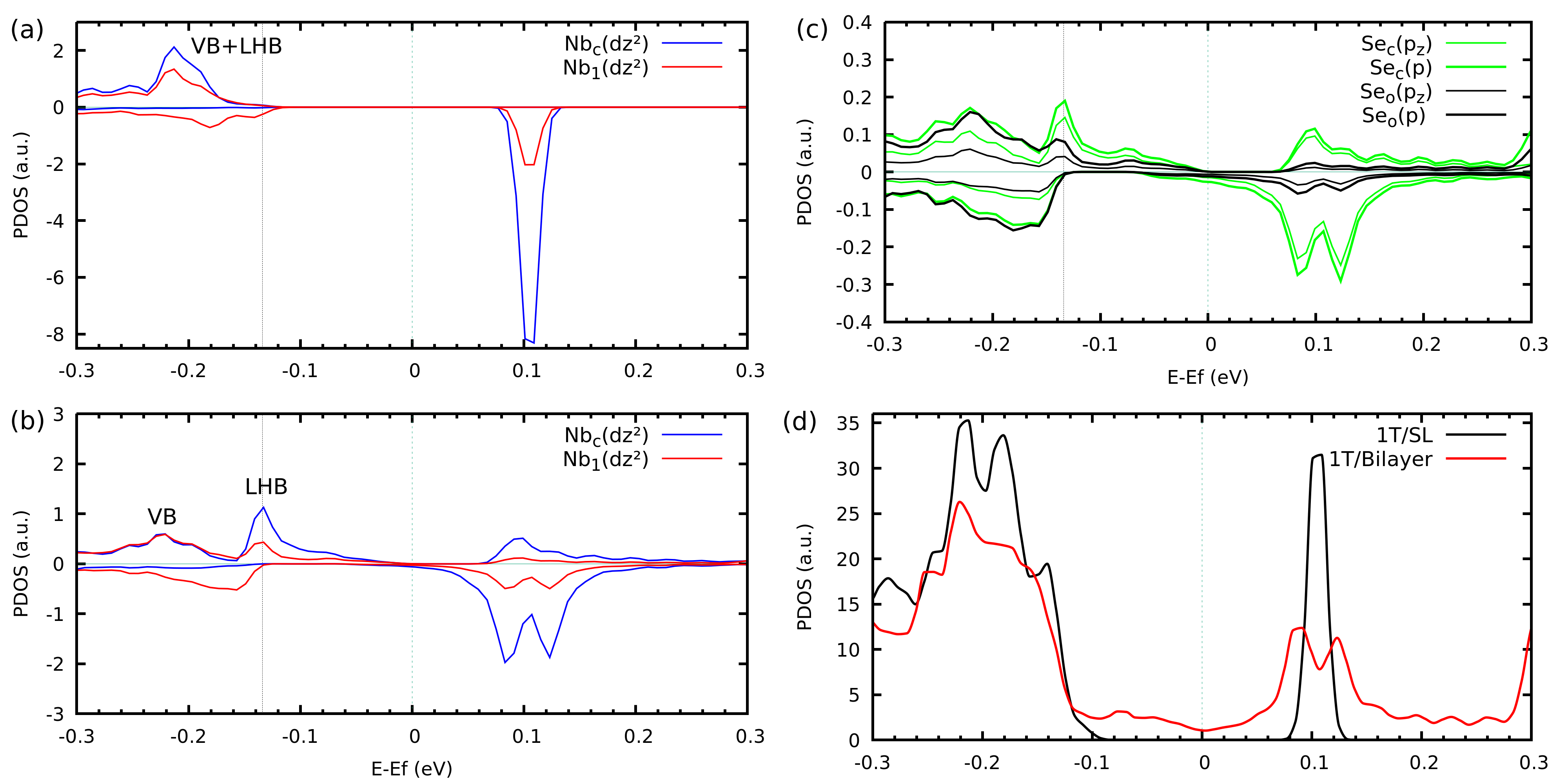
When we contrast the SL-1T with its bilayer counterpart (as depicted in Figure 4b), the previously observed broad peak al -0.22 eV undergoes a notable transformation, resolving into two distinct smaller peaks. The peak at -0.14 eV displays clear spin-polarized characteristics, primarily stemming from the involvement of Nb() and Se() orbitals (see Figure 4 b-c). Notably, the contribution from the Nbc SOD center exceeds that of its nearest neighbor Nb atoms, Nb1. These distinct features are also evident in the spatial distribution of the energy-resolved charge density (see Figure S4 in the SI). On the contrary, the peak positioned at -0.22 eV displays a diminished degree of spin polarization, embodying a more hybridized character. In this instance, Nbc and its nearest neighbor Nb atoms contribute almost equally, a trend consistently evident in the corresponding energy-resolved charge density (refer to Figure S4 in the Supplementary Information). Notably, this particular electronic structure spans a broader energy range, with a distinct and substantial contribution originating from Se() orbitals. All in all, our calculations suggest that the combined VB and LHB in the 1T-SL undergo a distinct separation when the 1T layer is in close proximity to the 1H layer. Specifically, the peak centered at -0.14 eV predominantly exhibits LHB characteristics, while the structure with a central energy of -0.22 eV displays a more pronounced Valence Band (VB) character.
The UHB in our observations also undergoes substantial alterations when compared to the Single-Layer (SL) case. Notably, we have observed that the UHB peak broadens and separates into two distinct components. The exact cause of this splitting remains unclear, as both peaks exhibit significant contributions from Nbc() states, along with contributions from their nearest neighbors (as evidenced in Figure 4b and further illustrated in Figure S4 in the Supplementary Information).
To further support the assignment of the LHB, VB and UHB we conducted a series of calculations using different Ueff parameters within our DFT+U framework. These calculations provided valuable insights into the behavior of these bands. Specifically, we observed that the peak associated with the LHB shifts towards lower energies, and the gap between the LHB and UHB increases as the Ueff values are elevated, in line with our expectations. Intriguingly, we also found that the splitting of the UHB is influenced by the Ueff parameter (for detailed visualization, refer to Figure S5 in the Supplementary Information).
The preceding discussion highlights the significant impact of the proximity between the 1T and 1H layers on the behavior of the LHB and UHB, resulting in their shifting closer to the Fermi level. This observed phenomenon can be attributed to the dielectric screening effects originating from the lower layer acting on the uppermost layer. This dielectric screening effectively reduces the on-site Coulomb repulsion (Hubbard U), thereby decreasing the energy gap between the LHB and the UHB111A similar reduction, attributed to the addition of extra layers, was also observed in 1T-TaSe2[45].. As a direct consequence of the reduction in U, a decrease in the charge within the majority spin is observed, along with an increase in the occupation of the Nbc(dz2) and Nb1(dz2) states in the minority spin. Importantly, this shift in charge distribution occurs while the overall total charge of the states remains relatively unchanged. This phenomenon serves to elucidate the underlying cause of the decrease in the magnetic moment of the SOD structure (additional details available in Figure S6 of the Supplementary Information).
The reduced on-site Coulomb repulsion U effectively decreases the gap between the Hubbard bands. In conjunction with their hybridization with the valence band, this leads to broadening, reduced localization, and extended tails. These effects contribute to the emergence of states at the Fermi level, consistent with the 1T phase’s transition towards a metallic phase. Evidence of this is seen in the PDOS for the 1T whole arrangement, as depicted in Figure 4d. The orbital composition of these states not only involves atoms and orbitals that are directly associated with the Hubbard bands. This observation strongly reinforces the idea that the overall system, rather than the Hubbard bands in isolation, plays a pivotal role in accounting for the population of these states and, consequently, for the insulating-to-metallic transition within the 1T phase in the bilayer system. This transition is a direct result of the proximity effect induced by the metallic 1H counterpart, reflecting the intricate interplay of electronic interactions within the system.
In summary, our findings indicate that the magnetic moment of the SOD persists within the heterostructure. Moreover, we find evidence of hybridization between 1T and 1H layers, along with a reduction in the effective Coulomb interaction, U, within the LHB and UHB. These characteristics align well with the scenario proposed by Liu et al. [8], where itinerant electrons in metallic 1H-NbSe2 couple with the spin of the SOD in 1T-NbSe2, resulting in the emergence of the Kondo screening effect.
IV Conclusions
In this theoretical investigation, we conducted a comprehensive study of 1T-NbSe2 and 1H-NbSe2 SLs and their heterobilayer structure by means of Density Functional Theory. Our findings indicate that a 1.3 eV and a lattice constant of 3.52 Å describe the overall physical properties of both SL configurations. For the 1T/1H heterobilayer, we explored the interlayer interaction between the SLs. Our investigation found a charge transfer and reorganization process between 1T and 1H layers of 0.17 flowing from the 1T phase to the 1H phase and supported by work function calculations. In particular, there is a concentration of charge at the interface between the 1T and 1H layers, primarily in the vicinity of the Se atoms. Upon bringing the 1T and 1H layers into close proximity, a discernible reduction in the magnetic moment of the star-of-David (SOD) structure is observed, diminishing from 0.72 to 0.43 . In the context of the 1T-SL, it is well-documented that the Valence Band (VB) and the Lower Hubbard Band (LHB) undergo hybridization, resulting in the formation of a broad peak. However, when the two SLs come into contact, this broad peak undergoes a notable transformation, splitting into two distinct structures. One is situated at -0.14 eV, characterized by clear LHB attributes, while the other, positioned at -0.22 eV, exhibits a diminished degree of spin polarization and a more hybridized character. The Upper Hubbard Band (UHB), which maintains a narrower profile in the SL, undergoes peak broadening while preserving its spin-polarized characteristics. This transformation of the electronic structure near the Fermi level is accompanied by a reduction in the Hubbard U, thanks to the dielectric screening effect between the layers. This reduction leads to an Insulator-to-Metal transition. In summary, the reduction in the effective Hubbard U and the broadening resulting from hybridization between single layers (SLs) with extended tails play a major role and provide a comprehensive explanation for the appearance of states at the Fermi level.
Acknowledgements.
R.P., I. H. and P.A. acknowledge the financial support from CONICET PIP-0083 and the computational time provided by the CCT-Rosario computational center and Computational Simulation Center (CSC) for Technological Applications, members of the High Performance Computing National System (SNCAD-MincyT Argentina). This work was also supported by the project PID2021-127917NB-I00 funded by MCIN/AEI/10.13039/501100011033, IT-1527-22 funded by the Basque Government, and 202260I187 funded by CSIC.Data availability statement
All data that support the findings of this study are included within the article (and any supplementary files).
References
- Novoselov et al. [2016] K. S. Novoselov, A. Mishchenko, A. Carvalho, and A. H. C. Neto, 2d materials and van der waals heterostructures, Science 353, aac9439 (2016), https://www.science.org/doi/pdf/10.1126/science.aac9439 .
- Geim and Grigorieva [2013] A. K. Geim and I. V. Grigorieva, Van der waals heterostructures, Nature 499, 419 (2013).
- Bernardi et al. [2017] M. Bernardi, C. Ataca, M. Palummo, and J. C. Grossman, Optical and electronic properties of two-dimensional layered materials, Nanophotonics 6, 479 (2017).
- Xi et al. [2016] X. Xi, Z. Wang, W. Zhao, J.-H. Park, K. T. Law, H. Berger, L. Forró, J. Shan, and K. F. Mak, Ising pairing in superconducting nbse2 atomic layers, Nature Physics 12, 139 (2016).
- Ugeda et al. [2016] M. M. Ugeda, A. J. Bradley, Y. Zhang, S. Onishi, Y. Chen, W. Ruan, C. Ojeda-Aristizabal, H. Ryu, M. T. Edmonds, H.-Z. Tsai, A. Riss, S.-K. Mo, D. Lee, A. Zettl, Z. Hussain, Z.-X. Shen, and M. F. Crommie, Characterization of collective ground states in single-layer nbse2, Nature Physics 12, 92 (2016).
- Guster et al. [2019] B. Guster, C. Rubio-Verdú, R. Robles, J. Zaldívar, P. Dreher, M. Pruneda, J. . Silva-Guillén, D.-J. Choi, J. I. Pascual, M. M. Ugeda, P. Ordejón, and E. Canadell, Coexistence of elastic modulations in the charge density wave state of 2h-nbse2, Nano Letters 19, 3027 (2019), pMID: 30998364, https://doi.org/10.1021/acs.nanolett.9b00268 .
- Lian et al. [2018] C.-S. Lian, C. Si, and W. Duan, Unveiling charge-density wave, superconductivity, and their competitive nature in two-dimensional nbse2, Nano Letters 18, 2924 (2018), pMID: 29652158, https://doi.org/10.1021/acs.nanolett.8b00237 .
- Liu et al. [2021a] M. Liu, J. Leveillee, S. Lu, J. Yu, H. Kim, C. Tian, Y. Shi, K. Lai, C. Zhang, F. Giustino, and C.-K. Shih, Monolayer 1t-nbse2 as a 2d-correlated magnetic insulator, Science Advances 7, eabi6339 (2021a), https://www.science.org/doi/pdf/10.1126/sciadv.abi6339 .
- Frindt [1972] R. F. Frindt, Superconductivity in ultrathin nb layers, Phys. Rev. Lett. 28, 299 (1972).
- Staley et al. [2009] N. E. Staley, J. Wu, P. Eklund, Y. Liu, L. Li, and Z. Xu, Electric field effect on superconductivity in atomically thin flakes of , Phys. Rev. B 80, 184505 (2009).
- Hamill et al. [2021] A. Hamill, B. Heischmidt, E. Sohn, D. Shaffer, K.-T. Tsai, X. Zhang, X. Xi, A. Suslov, H. Berger, L. Forró, F. J. Burnell, J. Shan, K. F. Mak, R. M. Fernandes, K. Wang, and V. S. Pribiag, Two-fold symmetric superconductivity in few-layer nbse2, Nature Physics 17, 949 (2021).
- Nakata et al. [2018] Y. Nakata, K. Sugawara, S. Ichinokura, Y. Okada, T. Hitosugi, T. Koretsune, K. Ueno, S. Hasegawa, T. Takahashi, and T. Sato, Anisotropic band splitting in monolayer nbse2: implications for superconductivity and charge density wave, npj 2D Materials and Applications 2, 12 (2018).
- Nakata et al. [2016] Y. Nakata, K. Sugawara, R. Shimizu, Y. Okada, P. Han, T. Hitosugi, K. Ueno, T. Sato, and T. Takahashi, Monolayer 1t-nbse2 as a mott insulator, NPG Asia Materials 8, 10.1038/am.2016.157 (2016), publisher Copyright: © 2016 The Author(s).
- Liu et al. [2023a] L. Liu, X. Song, X. Huang, H. Ji, Z. Hu, Y. Huang, H.-J. Gao, and Y. Wang, Review: Exploring spin properties in van der waals materials with star-of-david pattern, Materials Today Electronics 6, 100068 (2023a).
- Liebhaber et al. [2020] E. Liebhaber, S. Acero González, R. Baba, G. Reecht, B. W. Heinrich, S. Rohlf, K. Rossnagel, F. von Oppen, and K. J. Franke, Yu–shiba–rusinov states in the charge-density modulated superconductor nbse2, Nano Letters 20, 339 (2020), pMID: 31842547, https://doi.org/10.1021/acs.nanolett.9b03988 .
- Liu et al. [2023b] L. Liu, X. Song, J. Dai, H. Yang, Y. Chen, X. Huang, Z. Huang, H. Ji, Y. Zhang, X. Wu, J.-T. Sun, Q. Zhang, J. Zhou, Y. Huang, J. Qiao, W. Ji, H.-J. Gao, and Y. Wang, Unveiling electronic behaviors in heterochiral charge-density-wave twisted stacking materials with 1.25 nm unit dependence, ACS Nano 17, 2702 (2023b), pMID: 36661840, https://doi.org/10.1021/acsnano.2c10841 .
- Divilov et al. [2021] S. Divilov, W. Wan, P. Dreher, E. Bölen, D. Sánchez-Portal, M. M. Ugeda, and F. Ynduráin, Magnetic correlations in single-layer nbse2, Journal of Physics: Condensed Matter 33, 295804 (2021).
- Calandra [2018] M. Calandra, Phonon-assisted magnetic mott-insulating state in the charge density wave phase of single-layer , Phys. Rev. Lett. 121, 026401 (2018).
- Kresse and Hafner [1993a] G. Kresse and J. Hafner, Ab initio molecular dynamics for liquid metals, Phys. Rev. B 47, 558 (1993a).
- Kresse and Hafner [1993b] G. Kresse and J. Hafner, Ab initio molecular dynamics for open-shell transition metals, Phys. Rev. B 48, 13115 (1993b).
- Kresse and Furthmüller [1996a] G. Kresse and J. Furthmüller, Efficiency of ab-initio total energy calculations for metals and semiconductors using a plane-wave basis set, Comput. Mater. Sci. 6, 15 (1996a).
- Kresse and Furthmüller [1996b] G. Kresse and J. Furthmüller, Efficient iterative schemes for ab initio total-energy calculations using a plane-wave basis set, Phys. Rev. B 54, 11169 (1996b).
- Kresse and Joubert [1999] G. Kresse and D. Joubert, From ultrasoft pseudopotentials to the projector augmented-wave method, Phys. Rev. B 59, 1758 (1999).
- Hafner [2008] J. Hafner, Ab-initio simulations of materials using vasp: Density-functional theory and beyond, J. Comput. Chem. 29, 2044 (2008).
- Perdew et al. [1996] J. P. Perdew, K. Burke, and M. Ernzerhof, Generalized gradient approximation made simple, Phys. Rev. Lett. 77, 3865 (1996).
- Tkatchenko and Scheffler [2009] A. Tkatchenko and M. Scheffler, Accurate molecular van der waals interactions from ground-state electron density and free-atom reference data, Phys. Rev. Lett. 102, 073005 (2009).
- Dudarev et al. [1998] S. L. Dudarev, G. A. Botton, S. Y. Savrasov, C. J. Humphreys, and A. P. Sutton, Electron-energy-loss spectra and the structural stability of nickel oxide: An lsda+u study, Phys. Rev. B 57, 1505 (1998).
- Cococcioni and de Gironcoli [2005] M. Cococcioni and S. de Gironcoli, Linear response approach to the calculation of the effective interaction parameters in the method, Phys. Rev. B 71, 035105 (2005).
- Yu and Trinkle [2011] M. Yu and D. R. Trinkle, Accurate and efficient algorithm for bader charge integration, The Journal of Chemical Physics 134, 064111 (2011).
- Wickramaratne et al. [2020] D. Wickramaratne, S. Khmelevskyi, D. F. Agterberg, and I. I. Mazin, Ising superconductivity and magnetism in , Phys. Rev. X 10, 041003 (2020).
- Chen et al. [2021] Y. Chen, L. Liu, X. Song, H. Yang, Z. Huang, T. Zhang, H. Yang, H.-J. Gao, and Y. Wang, Twisted charge-density-wave patterns in bilayer 2d crystals and modulated electronic states, 2D Materials 9, 014007 (2021).
- Zhang et al. [2021] Q. Zhang, Y. Hou, T. Zhang, Z. Xu, Z. Huang, P. Yuan, L. Jia, H. Yang, Y. Huang, W. Ji, J. Qiao, X. Wu, and Y. Wang, Visualizing spatial evolution of electron-correlated interface in two-dimensional heterostructures, ACS Nano 15, 16589 (2021), pMID: 34606233, https://doi.org/10.1021/acsnano.1c06332 .
- Liu et al. [2023c] L. Liu, X. Song, J. Dai, H. Yang, Y. Chen, X. Huang, Z. Huang, H. Ji, Y. Zhang, X. Wu, J.-T. Sun, Q. Zhang, J. Zhou, Y. Huang, J. Qiao, W. Ji, H.-J. Gao, and Y. Wang, Unveiling electronic behaviors in heterochiral charge-density-wave twisted stacking materials with 1.25 nm unit dependence, ACS Nano 17, 2702 (2023c), pMID: 36661840, https://doi.org/10.1021/acsnano.2c10841 .
- Liu et al. [2021b] Z.-Y. Liu, S. Qiao, B. Huang, Q.-Y. Tang, Z.-H. Ling, W.-H. Zhang, H.-N. Xia, X. Liao, H. Shi, W.-H. Mao, G.-L. Zhu, J.-T. Lü, and Y.-S. Fu, Charge Transfer Gap Tuning via Structural Distortion in Monolayer 1T-NbSe2, Nano Letters 21, 7005 (2021b).
- Liu et al. [2019] Y. Liu, Y. Huang, and X. Duan, Van der waals integration before and beyond two-dimensional materials, Nature 567, 323 (2019).
- Liu et al. [2023d] Y. Liu, Y. Feng, L. Hu, X. Wu, S. Qiao, and G. Gao, Structural, electronic phase transitions and thermal spin transport properties in 2d nbse2 and nbs2: a first-principles study, Phys. Chem. Chem. Phys. 25, 1632 (2023d).
- Huang et al. [2022] Z. Huang, X. Song, Y. Chen, H. Yang, P. Yuan, H. Ma, J. Qiao, Y. Zhang, J. Sun, T. Zhang, Y. Huang, L. Liu, H.-J. Gao, and Y. Wang, Size dependence of charge-density-wave orders in single-layer nbse2 hetero/homophase junctions, The Journal of Physical Chemistry Letters 13, 1901 (2022), pMID: 35179388, https://doi.org/10.1021/acs.jpclett.1c04138 .
- Kezilebieke et al. [2020] S. Kezilebieke, M. N. Huda, P. Dreher, I. Manninen, Y. Zhou, J. Sainio, R. Mansell, M. M. Ugeda, S. van Dijken, H.-P. Komsa, and P. Liljeroth, Electronic and magnetic characterization of epitaxial vse2 monolayers on superconducting nbse2, Communications Physics 3, 116 (2020).
- Hu et al. [2018] X. Hu, Y. Wang, X. Shen, A. V. Krasheninnikov, L. Sun, and Z. Chen, 1t phase as an efficient hole injection layer to tmds transistors: a universal approach to achieve p-type contacts, 2D Materials 5, 031012 (2018).
- Zhang et al. [2022] H. Zhang, A. Rousuli, K. Zhang, L. Luo, C. Guo, X. Cong, Z. Lin, C. Bao, H. Zhang, S. Xu, R. Feng, S. Shen, K. Zhao, W. Yao, Y. Wu, S. Ji, X. Chen, P. Tan, Q.-K. Xue, Y. Xu, W. Duan, P. Yu, and S. Zhou, Tailored ising superconductivity in intercalated bulk nbse2, Nature Physics 18, 1425 (2022).
- Dai et al. [2023] J. Dai, J. Qiao, C. Wang, L. Zhou, X. Wu, L. Liu, X. Song, F. Pang, Z. Cheng, X. Kong, Y. Wang, and W. Ji, Layer sliding and twisting induced electronic transitions in correlated magnetic 1t-nbse2 bilayers, Advanced Functional Materials 33, 2302989 (2023), https://onlinelibrary.wiley.com/doi/pdf/10.1002/adfm.202302989 .
- Crippa et al. [2024] L. Crippa, H. Bae, P. Wunderlich, I. I. Mazin, B. Yan, G. Sangiovanni, T. Wehling, and R. Valentí, Heavy fermions vs doped mott physics in heterogeneous ta-dichalcogenide bilayers, Nature Communications 15, 1357 (2024).
- Liu et al. [2021c] L. Liu, H. Yang, Y. Huang, X. Song, Q. Zhang, Z. Huang, Y. Hou, Y. Chen, Z. Xu, T. Zhang, X. Wu, J. Sun, Y. Huang, F. Zheng, X. Li, Y. Yao, H.-J. Gao, and Y. Wang, Direct identification of mott hubbard band pattern beyond charge density wave superlattice in monolayer 1t-nbse2, (2021c).
- Note [1] A similar reduction, attributed to the addition of extra layers, was also observed in 1T-TaSe2[45].
- Chen et al. [2020] Y. Chen, W. Ruan, M. Wu, S. Tang, H. Ryu, H.-Z. Tsai, R. L. Lee, S. Kahn, F. Liou, C. Jia, O. R. Albertini, H. Xiong, T. Jia, Z. Liu, J. A. Sobota, A. Y. Liu, J. E. Moore, Z.-X. Shen, S. G. Louie, S.-K. Mo, and M. F. Crommie, Strong correlations and orbital texture in single-layer 1t-tase2, Nature Physics 16, 218 (2020).