Microelectronic readout of a diamond quantum sensor
Abstract
Quantum sensors based on the nitrogen-vacancy (NV) centre in diamond are rapidly advancing from scientific exploration towards the first generation of commercial applications. While significant progress has been made in developing suitable methods for the manipulation of the NV centre spin state, the detection of the defect luminescence has so far limited the performance of miniaturized sensor architectures. The recent development of photoelectric detection of the NV centre’s spin state offers a path to circumvent these limitations, but has to-date required research-grade low current amplifiers to detect the picoampere-scale currents obtained from these systems. Here we report on the photoelectric detection of magnetic resonance (PDMR) with NV ensembles using a complementary metal-oxide semiconductor (CMOS) device. The integrated circuit delivers a digitized output of the diamond sensor with low noise and 50 femtoampere resolution. This integration provides the last missing component on the path to a compact, diamond-based quantum sensor. The device is suited for continuous wave (CW) as well as pulsed operation. We demonstrate its functionality with DC and AC magnetometry up to several megahertz, coherent spin rotation and multi-axial decoupling sequences for quantum sensing.
I Introduction
Device miniaturization and integration opens up new perspectives for applications of quantum sensors based on atom-like systems in crystals [1, 2, 3, 4, 5, 6, 7, 8]. Based on its excellent spin coherence time, greater than 1.8 ms for a single NV [9], its optically addressable spin state, and its large dynamic range, the nitrogen-vacancy (NV) centre in diamond [10] is now firmly established as a room-temperature quantum sensor for crystal stress [11], pressure [12], electric fields [13], temperature [14], and magnetic fields [15, 16, 17, 18, 19, 20], including nuclear magnetic resonance spectroscopy [21, 22].
Such systems reach excellent sensitivity, resolution, bandwidth and range, but commonly require large and costly instruments for their manipulation and readout. These factors have so far limited their adoption to highly specialized applications and also hinder the scalability with respect to the number of sensor elements on a single device. Therefore in recent years, significant efforts have been undertaken towards the miniaturization of NV-based sensors [8, 23, 1, 24] including their required periphery. Typically, the form factor is strongly affected by the microwave chain, including bulky, high-power amplifiers, and by the optical components required to read out the NV centre’s spin state. Regarding spin control, it has been shown that microwave generation can be realized directly on a silicone (Si) chip underneath the diamond [1]. Furthermore, the use of microwave resonators can provide a way to effectively reduce the necessary amplifier size and power at the cost of bandwidth [25]. The optical excitation and detection system typically includes a green (510 - ) excitation laser and single-photon counting modules (SPCM) to collect the red NV centre fluorescence. The excitation apparatus can already be reduced in size by making use of directly driven laser diodes [26], and the integration of the diamond sensor on, or in proximity of, an optical fiber tip has also been explored [27, 28, 24].
However, optical detection suffers from the high refractive index of diamond, such that typically only a few percent of the emitted photons actually reach the detectors. This has, to a degree, been circumvented by elaborate surface engineering such as focused ion beam milled solid immersion lenses with NV centres at their centre [29, 30] as well as small-scale photodiodes in close proximity to the NV-based sensor [24, 8]. However, all of these systems still lack a compact and robust readout system for the NV centre spin state that can be scaled down to the few- or even single-defect level.
The advent of photoelectric detection of the NV centre’s spin state presents a viable path towards integrated electronic detection [31, 32, 33, 34, 35, 36, 37]. Charge carriers are generated at the NV centre in a two-photon ionization process by laser illumination which, in contrast to optical detection, relies on the direct capture of charge carriers through electrodes fabricated onto the diamond surface and does not suffer from total internal reflection due to the relatively high refractive index of diamond. Photoelectric readout furthermore offers the potential to avoid the limiting saturation behavior of optical readout, since the charge carrier generation can occur at a far higher rate than photoemission [38]. Chiefly, this method obviates the need for bulky collection optics and mitigates the detrimental effect of the high refractive index on signal acquisition.
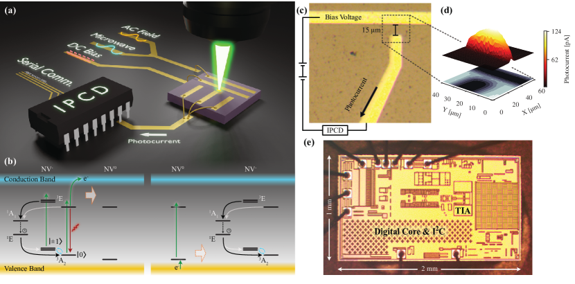
Here we report on the miniaturization and circuit integration of an NV centre based sensor through photocurrent detection with state-of-the-art microchip technology (see Fig. 1a). The small-footprint device features low readout noise, high resolution and a photocurrent signal on the order of , which is detected at room temperature by an integrated photocurrent detector (IPCD). We demonstrate the functionality of the device by detecting both DC and AC magnetic fields, with frequencies larger than one MHz, as well as performing an exemplary decoupling sequence towards advanced quantum sensing applications.
II Photocurrent detection of the nitrogen-vacancy centre
The NV centre is formed by replacing two adjacent carbon atoms within the diamond lattice by a nitrogen atom and a vacancy. This configuration forms a stable, atom-sized defect with a triplet ground state. Optically induced spin polarization and spin-dependent fluorescence enable remarkable spin purity and readout contrast, even at room temperature [39, 40]. The ground state features a zero-field splitting of between the and sub-levels which can be manipulated via magnetic resonance. The resonance frequencies between the and sub-levels are sensitive to electric and magnetic fields as well as to crystal strain and temperature. In particular, external magnetic fields parallel to the N-V axis induce a Zeeman splitting of the states given by
| (1) |
where is the electronic gyromagnetic ratio of and the -component of the magnetic field measured along the NV centre symmetry axis [10]. Since, due to geometrical constrains within the diamond lattice, NV centres can only be oriented along four axes, ensembles of NV centres can be used to perform vector magnetometry [41, 42, 43].
While optical excitation of the sub-level preferentially results in photon emission, the populations decay to a meta-stable level with a branching ratio close to 0.5, reducing the fluorescence from these states and allowing spin state readout (see Fig. 1b). Furthermore, the meta-stable level decays to both and , though preferentially towards , leading to state initialization [10, 40]. These mechanisms allow optical detection of magnetic resonances (ODMR), where fluorescence collection upon excitation will decrease if a resonant microwave signal is applied to transfer population from to or .
Similarly to fluorescence readout, in electrical readout the state is mostly not shelved into the meta-stable state and can thus produce more charge carriers via two-photon excitation (see Fig. 1b). The excited states instead decay frequently to the long-lived and dark metastable state which has a far smaller ionization cross-section than . The basic ODMR method described above can therefore be used without alteration for photoelectric detection of magnetic resonances (PDMR), as shown in Fig. 1b.
III On-chip photocurrent detection
Charge carrier collection is enabled by the application of a bias electric field across the electrode gap, as shown in Fig. 1c and d. We use a voltage of up to over a gap of 15 micrometers, produced by a stack of coin cell batteries, resulting in a field gradient of . This value is safely below the limiting value of given by the breakthrough voltage of air under standard conditions obtained from Paschen’s law [44]. Cell batteries were chosen for compactness as a low-noise power supply.
The photocurrent is detected by a non-commercial microchip from Infineon Technologies, which acts as an integrated photocurrent detector (IPCD), amplifier, integrator, and digitizer [45]. Its small packaged footprint of only allows to position it in close proximity to the diamond chip (see Fig. 1a for an abstract representation of the setup, and Fig. 1e for a microscope image of the bare chip). The low-noise, ultra-low power (sub-mW) chip offers a 16 bit analog to digital converter with a least-significant-bit (LSB) equivalent current of , a measurement standard deviation of 1.2 LSB, and an integration time of (see the supplementary information for more details [46]). The chip is powered by a low noise linear regulator at (ADP150AUJZ-1.8-R7) and addressed as well as read out by a microcontroller, which acts only as an I2C-converter to enable communication with the measurement computer.
Fig. 1d shows a simultaneous fluorescence (bottom) and photocurrent (top) scan over the electrodes where the fluorescence counts and the photocurrent are detected for each position. A clear peak in photocurrent is visible in the middle of the gap between the current detector and bias wires. The fluorescence image shows a clear negative image of the deposited structures.
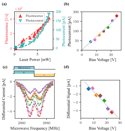
In order to investigate the performance of the IPCD, we perform characterization measurements on the optical and photoelectric characteristics of the diamond sample. First, we perform a saturation scan where we gradually increase the continuous wave (CW) laser power while simultaneously measuring both fluorescence and photocurrent (Fig. 2a). While the power dependence of the fluorescence is consistent with a linear trend, the photocurrent dependence displays the quadratic behaviour expected from the two-photon process involved in charge state conversion (see Fig. 1b). We chose excitation power in all subsequent measurements (see SI for further information [46]). Fig. 2b shows the detected photocurrent while varying the bias voltage across the electrode gap. A linear dependence with respect to the applied bias voltage is observed.
We furthermore probe the to transitions using an external microwave for seven different bias voltages with no applied magnetic bias field (Fig. 2c) where an intrinsic splitting of between the two spin transitions is discernible. Here, the sequence was divided into two parts: In the first half we include the CW microwave together with CW laser excitation while the second half consists of the readout laser alone. Subtraction of the two sequence segments results in a differential signal which increases linearly with the bias voltage (Fig. 2d).
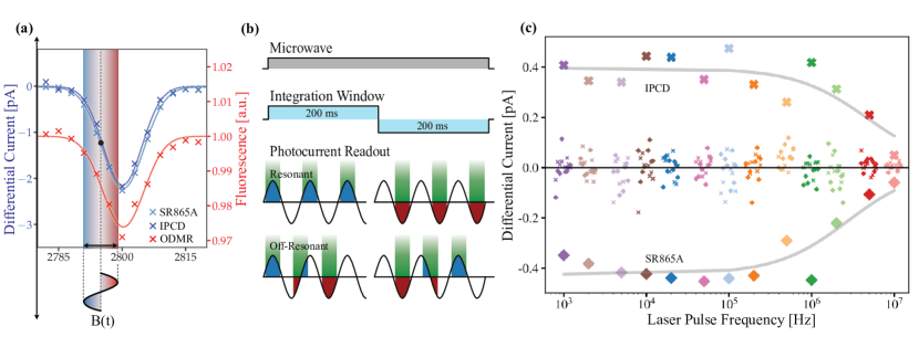
In a further measurement, the performance of the IPCD is compared to a high-end commercial lock-in amplifier (SRS SR865A). The settings of the commercial device are chosen to match the IPCD parameters as closely as possible. The input impedance is set to and, as in the case of the IPCD measurements, a lock-in frequency of 2 Hz is used, with a time constant of 300 ms and a sensitivity of . We change the bias magnetic field to energetically split the ground state levels equally for all NV centre axis orientations in the ensemble sample to maximize the photoelectric spin signal and allow better distinguishability of resonance shifts under external magnetic fields examined in the next section. The green laser is operated at constant intensity, while the microwave signal is scanned in frequency over the resonance. As above, the photocurrent is extracted in a two-step procedure: a segment with microwave signal is followed by a second segment without microwave. The photocurrent readouts of both are subtracted and are shown in Fig. 3a. The measurement shows near-identical results for the IPCD and the commercial lock-in amplifier.
IV Pulsed-Excitation AC Magnetometry
To demonstrate the IPCDs capability for AC magnetometry, a sinusoidally-varying current is applied to a wire adjacent to the detection site. The AC signal is generated by a 10 Volt AC source over a dump resistor, resulting in a magnetic field peak-to-peak amplitude of 3.2 G at the readout junction. In order to detect the frequency of this field, we choose the microwave frequency offset for the measurement to coincide with the highest derivative of the resonance signal with respect to magnetic field changes, as indicated by the dotted vertical line in Fig. 3a. A maximum conversion factor of is obtained there. The measurement sequence is illustrated in Fig. 3b. In order to detect periodic magnetic field variations with periods much shorter than the photocurrent integration window, we implement a method which we term pulsed-laser stroboscopic detection (PLSD) method: The excitation laser is modulated with square-wave pulses at the target detection frequency. We adjust the pulse duration to cover 1/4 of the target AC field period. PLSD operates in a phase-locked manner, where the readout sequence is again split into two segments. The optical pulses for photocurrent generation are shifted by a phase of in the second segment. If the readout is performed resonantly with the AC-field oscillation, the current difference between the two segments will be maximal, while off resonance (and with many repetitions of readout pulses per segment) the obtained currents in the segments average out to zero. Similarly to quantum heterodyne detection or coherently averaged synchronized readout, the frequency resolution of PLSD is not limited by the coherence lifetime of the NV centres [47, 22]. We further note that, by including all four quadratures instead of only two, it is possible to measure AC fields of arbitrary phase with this approach, at the cost of doubling the readout duration.
The results of the PLSD measurements are shown in Fig. 3c. We sweep the laser pulse frequency to probe several external AC fields and keep the laser pulse width constant while varying the inter-pulse distance (see Fig. 3b). We obtain clear signal peaks whenever the pulsed laser readout has the same frequency as the external field. Here, the current values for the SR865A are mirrored around the -axis for better visibility. The two devices measure near-identical currents on resonance (large markers in the figure) while showing no significant current when detuned (small symbols). The measurement covers over four orders of magnitude in frequency and demonstrates that PLSD allows to measure AC fields with a bandwidth of .
V Coherent spin manipulation
While so far, the microwave signal was operated in a continuous fashion and the laser was pulsed for AC magnetometry, many sensing applications using the NV centre strongly benefit from the application of pulsed spin rotation sequences [20, 48, 47]. We thus show that the integrated chip is suitable for pulsed-sequence readout by detecting coherent rotations of the spins.
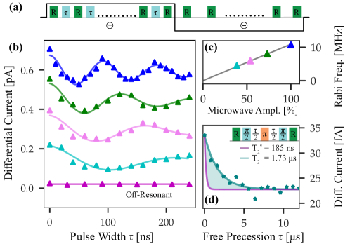
To mitigate inhomogeneous driving and remove the spectral overlap of the four NV orientations in the high-density sample, we first single out one NV orientation using a neodymium magnet to apply a bias field along one of the crystalline orientations. Using the same measurement envelope as in Fig. 2c, we alternate laser and microwave pulses while varying the microwave pulse length (see Fig. 4a). Fig. 4b shows Rabi oscillations with four different microwave powers. We obtain the expected sinusoidal signal (solid lines) with an additional damping due to the coherence time of the sample. Furthermore, the expected linear relationship between microwave amplitude and Rabi frequency is visible in Fig 4c. We additionally perform a measurement under full microwave power, off resonance from the to transition, where no change in photocurrent versus pulse width is observed. This measurement shows that there is negligible cross-talk between the high-power microwave line and the IPCD (darker pink line and data points in Fig. 4b).
The most advanced quantum sensing methods make use of multi-axial decoupling methods to minimize the effects of stray magnetic fields and control pulse imperfections [49]. Fig. 4d shows the results when applying a Carr-Purcell-Meiboom-Gill (CPMG) sequence in order to determine the coherence time of the sample. Compared to the CW-microwave, pulsed-laser method shown in Fig. 3, this method enables to sense external fields at arbitrary frequencies, ranging from DC to an upper limit given by the hardware limit determined only by the attainable Rabi frequency. First, a pulse about the -axis of the Bloch sphere rotates the initial state into a coherent superposition of and . During a subsequent free precession time of length , the superposition will rotate unpredictably along the equator of the Bloch sphere due to magnetic field noise from adjacent spins and external sources. Those external disturbances lead to the comparatively short coherence time extracted from the decay envelope of the Rabi oscillations in Fig. 4b. However, subsequent application of a pulse about the orthogonal axis, followed by an additional free precession time allows the reversal of a large part of these dephasing mechanisms. The sequence is concluded by a pulse which, were it not for irreversible decoherence processes, would lead to a near-complete spin state transfer from to . The pulses are generated by a field programmable gate array (FPGA) [50]. We obtain a coherence time of , corresponding to an improvement by more than an order of magnitude compared to the bare dephasing time . This sequence can already be used to sense external AC magnetic fields with high sensitivity [20].
We note here that lock-in based methods such as photoelectric detection presently integrate over the entire laser pulse duration, while optical detection allows to select the relevant time window of at the beginning of the readout pulse, allowing to optimize the optical readout contrast [51, 40]. Fast gating methods for the electrical readout current are therefore of great interest for further improvement of the technique.
VI Discussion and Conclusion
This work combines several milestones for diamond quantum sensors on the path from the laboratory towards practical applications. Together with previous demonstrations, including small-scale optical excitation [8] and chip-integrated microwave generation [1, 23] to manipulate the spin state, the integration of electrical readout of the NV centre spin state shown in this work completes the foundation for extremely compact, low-power quantum sensors. The implemented device is CMOS compatible and enables photoelectric readout of nitrogen vacancy centres in diamond with sufficiently low noise and high current resolution to even enable the readout of single centres [35]. Due to its low noise and large dynamic range, the IPCD can be used to read out both continuous-wave and pulsed sequences, frequently encountered in quantum sensing applications. The IPCD achieves near-identical performance as a state-of-the-art lock-in amplifier, demonstrating both DC as well as AC magnetometry. The DC sensitivity of reached (see methods) in this first demonstration already compares favorably with previous approaches [1], while necessitating far lower excitation power, and can be improved dramatically with optimized substrates [38]. Furthermore, the first stepping stones towards the use of more complex dynamical decoupling schemes are shown, underscoring the functionality of the device for a broad range of diamond quantum sensor applications.
The combination with board- or chip-level integration of optical excitation, microwave generation, and sequence control will complete the development towards miniaturized, high-performance diamond quantum sensors based on photoelectric readout.
VII Methods
VII.1 Fabrication and Setup
A high-pressure, high-temperature (HPHT) diamond from Element-6 with a nitrogen concentration 200 ppm served as the NV centre host. It was electron irradiated at 100°C and annealed at 900°C to increase NV centre yield and resulting in an NV concentration of ppm. After cleaning in a mixture of potassium nitrate and sulfuric acid, followed by repeated cleaning in solvents (acetone, isopropanol, ethanol, and methanol) the sample was further left in oxygen plasma for five minutes at 100 W. Subsequently, a custom-made silicon hard mask was positioned on it, immediately followed by another oxygen plasma cleaning step and metal deposition. First, a layer of titanium was sputtered onto the sample, followed by of thermally evaporated copper and of gold to avoid oxidation of the copper layer. The electrode arrangement is shown in Fig. 1c. The width of the wires and the gap size are both .
After deposition, the sample was repeatedly cleaned in the previously mentioned solvents, mounted and bonded onto a printed circuit board (PCB), with electrical connections formed by thick aluminium bond wires (details in supplementary information [46]). The PCB provides an electrical interface to our measurement and manipulation hardware, as well as to the commercial lock-in amplifier for device comparison [46]. While currently a microcontroller reads out each part of the differential signal and the values are subtracted in the measurement computer, the IPCD can be altered to provide the background subtracted signal directly, obviating the need for the microcontroller. This direct lock-in mode is already available, albeit with an unsuitable combination of lock-in frequency and signal gain. Furthermore, a built-in feature of the IPCD is given by a synchronous TTL output, in phase with the lock-in cycle, which can be used to directly control the laser driver or microwave switch such that no external TTL source would be required.
In order to compare photoelectric readout to conventional, optically detected magnetic resonance, the PCB was mounted into a confocal microscope setup using an Olympus microscope objective with a numerical aperture of 0.85. A laser diode provided green excitation, necessary for spin initialization and readout, with a maximum power of . The photoluminescence was filtered with a longpass filter. We underline that, while collection path filtering and photodetection are not needed for electrical readout, an excitation path which provides a sufficiently high intensity (on the order of ) remains necessary.
The microwave signal necessary to drive the spin transitions was generated by an Analog Devices ADF4351 RF synthesizer, switched using a Mini-Circuits ZASWA2-50-DR+ RF switch, and amplified by with a Mini-Circuits ZHL-16W-43+ high power amplifier. The amplified signal was combined with an AC source (0-500 MHz) used for the PLSD measurements using a custom made diplexer (Wainwright Instruments). The combined signal output was connected to the PCB, reaching the the microfabricated wire on the diamond chip through a bond wire.
VII.2 Comparison of Photoelectric and Optical Readout
In photoluminescence readout, we observe a photon collection rate of cts/s from the NV ensemble after reducing the collection efficiency with neutral density (ND) filters by 5.7 orders of magnitude, and including all system losses. Removing the ND filters would result in a rate of cts/s. The minimum detectable field in a CW ODMR magnetometry measurement for small fields is given by [20]
| (2) |
where is the full width at half-maximum of the lineshape, the Planck constant, g the Landé factor, the Bohr magneton, the readout contrast and the average detection rate. The angle between the NV centre axis and the applied field leads to an increase of . The factor accounts for the equal bisection of the sequence into a measurement part, with the microwave field applied, and a normalization measurement without. Using the values from the measurement in Fig. 3 (, %), we find a raw sensitivity for optical detection of , while correcting for the attenuation by the ND filters yields a nominal sensitivity of . The nominal sensitivity for electrical readout results instead from the rate of charge carriers collected in the system. There, with an average photocurrent of , the rate is s-1 yielding a sensitivity of .
The sensitivity of the PLSD measurements at a frequency is reduced by the duty cycle of , with the duration of the illumination pulse. Additionally, the average detected field during a readout pulse is reduced, compared to a DC field, because of the sinusoidal time dependence. However, both portions of the sequence are used to measure the magnetic field, improving the sensitivity by . These factors lead to a minimum detectable field of
| (3) |
We use a duty cycle of %, resulting in a nominal sensitivity of .
All sensitivity values achieved here can be improved significantly by optimizing the material properties of the diamond. The defect density is a key parameter: For decreasing nitrogen and NV centre density, the spin resonance linewidth decreases and the photocurrent per NV centre increases, while the photoluminescence per NV centre remains constant. It will therefore be possible to generate similar photocurrents while drastically reducing the spin resonance linewidth, thus improving the sensitivity of the device, by using tailored diamond substrates. Furthermore, recent experiments under similar conditions on a different diamond have resulted in a photocurrent of at similar laser powers, translating to a sensitivity improvement by an order of magnitude [38].
Even better sensitivity is possible using a larger detection volume and higher excitation power [52]. From the obtained photon count rate and estimated NV centre density in our sample we calculate the sensor volume using our excitation beam to be . However, we note that the volume extracted from photon collection will most likely be larger than the actual interrogation volume available for photocurrent detection, due to the latter’s quadratic dependence on laser power. Nonetheless, using this conservative estimate, fabrication of interdigitated electrodes across the entire diamond surface would allow to improve the sensitivity significantly: For a interrogation volume, the nominal sensitivity would improve by another 5 orders of magnitude, reaching . Further improvement towards and below will be possible using NV ensembles with narrower spin resonance linewidth and optimized photocurrent collection.
VII.3 Noise Estimation
The IPCD exhibits a noise floor of 1.2 least-significant bits (LSB), corresponding to a nominal noise floor of which represents the largest of the contributing noise factors. The electron shot noise at is , an order of magnitude smaller than the bit noise, and the thermal Johnson-Nyquist noise is . Inherent noise factors are thus still almost two orders of magnitude below our detected differential signal of in CW-PDMR. The relative noise floor can be reduced by increasing the photoelectric signal, either by use of a different diamond host that produces a larger photoelectric current, or by implementing low-noise, chip-scale pre-amplification of the obtained signal[53].
VIII Acknowledgments
We wish to acknowledge the support from the FFG via projects 870002 (QSense4Life) and 877615 (QSense4Power), and the QuantERA FFG project 864036 (Q-Magine). This project has received funding from the European Union’s Horizon Europe research and innovation program under Grant Agreement No. 101046911 (QuMicro). We thank J. Pribošek, K. Harms, T. Moldaschl, G. Auböck, C. Hirschl, F. Starmans, and F. Michl for useful discussions.
Conflict of Interest: The authors declare no conflict of interest.
References
- Kim et al. [2019] D. Kim, M. I. Ibrahim, C. Foy, M. E. Trusheim, R. Han, and D. R. Englund, A cmos-integrated quantum sensor based on nitrogen–vacancy centres, Nature Electronics 2, 284 (2019).
- Liu et al. [2013] X. Liu, J. Cui, F. Sun, X. Song, F. Feng, J. Wang, W. Zhu, L. Lou, and G. Wang, Fiber-integrated diamond-based magnetometer, Applied Physics Letters 103, 143105 (2013).
- Patel et al. [2016] R. N. Patel, T. Schröder, N. Wan, L. Li, S. L. Mouradian, E. H. Chen, and D. R. Englund, Efficient photon coupling from a diamond nitrogen vacancy center by integration with silica fiber, Light: Science & Applications 5, e16032 (2016).
- Fedotov et al. [2016] I. Fedotov, S. Blakley, E. Serebryannikov, P. Hemmer, M. Scully, and A. Zheltikov, High-resolution magnetic field imaging with a nitrogen-vacancy diamond sensor integrated with a photonic-crystal fiber, Optics letters 41, 472 (2016).
- Chatzidrosos et al. [2017] G. Chatzidrosos, A. Wickenbrock, L. Bougas, N. Leefer, T. Wu, K. Jensen, Y. Dumeige, and D. Budker, Miniature cavity-enhanced diamond magnetometer, Physical Review Applied 8, 044019 (2017).
- Barson et al. [2017] M. S. Barson, P. Peddibhotla, P. Ovartchaiyapong, K. Ganesan, R. L. Taylor, M. Gebert, Z. Mielens, B. Koslowski, D. A. Simpson, L. P. McGuinness, et al., Nanomechanical sensing using spins in diamond, Nano letters 17, 1496 (2017).
- Webb et al. [2019] J. L. Webb, J. D. Clement, L. Troise, S. Ahmadi, G. J. Johansen, A. Huck, and U. L. Andersen, Nanotesla sensitivity magnetic field sensing using a compact diamond nitrogen-vacancy magnetometer, Applied Physics Letters 114, 231103 (2019).
- Stürner et al. [2019] F. M. Stürner, A. Brenneis, J. Kassel, U. Wostradowski, R. Roelver, T. Fuchs, K. Nakamura, H. Sumiya, S. Onoda, J. Isoya, et al., Compact integrated magnetometer based on nitrogen-vacancy centres in diamond, Diamond and Related Materials 93, 59 (2019).
- Balasubramanian et al. [2009] G. Balasubramanian, P. Neumann, D. Twitchen, M. Markham, R. Kolesov, N. Mizuochi, J. Isoya, J. Achard, J. Beck, J. Tissler, et al., Ultralong spin coherence time in isotopically engineered diamond, Nature materials 8, 383 (2009).
- Doherty et al. [2013] M. W. Doherty, N. B. Manson, P. Delaney, F. Jelezko, J. Wrachtrup, and L. C. Hollenberg, The nitrogen-vacancy colour centre in diamond, Physics Reports 528, 1 (2013).
- Grazioso et al. [2013] F. Grazioso, B. R. Patton, P. Delaney, M. L. Markham, D. J. Twitchen, and J. M. Smith, Measurement of the full stress tensor in a crystal using photoluminescence from point defects: The example of nitrogen vacancy centers in diamond, Applied Physics Letters 103, 101905 (2013).
- Doherty et al. [2014] M. W. Doherty, V. V. Struzhkin, D. A. Simpson, L. P. McGuinness, Y. Meng, A. Stacey, T. J. Karle, R. J. Hemley, N. B. Manson, L. C. Hollenberg, et al., Electronic properties and metrology applications of the diamond nv- center under pressure, Physical review letters 112, 047601 (2014).
- Dolde et al. [2011a] F. Dolde, H. Fedder, M. W. Doherty, T. Nöbauer, F. Rempp, G. Balasubramanian, T. Wolf, F. Reinhard, L. C. Hollenberg, F. Jelezko, et al., Electric-field sensing using single diamond spins, Nature Physics 7, 459 (2011a).
- Plakhotnik et al. [2014] T. Plakhotnik, M. W. Doherty, J. H. Cole, R. Chapman, and N. B. Manson, All-optical thermometry and thermal properties of the optically detected spin resonances of the nv–center in nanodiamond, Nano letters 14, 4989 (2014).
- Acosta et al. [2010] V. M. Acosta, E. Bauch, M. P. Ledbetter, A. Waxman, L.-S. Bouchard, and D. Budker, Temperature dependence of the nitrogen-vacancy magnetic resonance in diamond, Physical review letters 104, 070801 (2010).
- Dolde et al. [2011b] F. Dolde, H. Fedder, M. W. Doherty, T. Nöbauer, F. Rempp, G. Balasubramanian, T. Wolf, F. Reinhard, L. C. Hollenberg, F. Jelezko, et al., Electric-field sensing using single diamond spins, Nature Physics 7, 459 (2011b).
- Degen [2008] C. Degen, Scanning magnetic field microscope with a diamond single-spin sensor, Applied Physics Letters 92, 243111 (2008).
- Balasubramanian et al. [2008] G. Balasubramanian, I. Chan, R. Kolesov, M. Al-Hmoud, J. Tisler, C. Shin, C. Kim, A. Wojcik, P. R. Hemmer, A. Krueger, et al., Nanoscale imaging magnetometry with diamond spins under ambient conditions, Nature 455, 648 (2008).
- Maze et al. [2008] J. R. Maze, P. L. Stanwix, J. S. Hodges, S. Hong, J. M. Taylor, P. Cappellaro, L. Jiang, M. G. Dutt, E. Togan, A. Zibrov, et al., Nanoscale magnetic sensing with an individual electronic spin in diamond, Nature 455, 644 (2008).
- Rondin et al. [2014] L. Rondin, J.-P. Tetienne, T. Hingant, J.-F. Roch, P. Maletinsky, and V. Jacques, Magnetometry with nitrogen-vacancy defects in diamond, Reports on Progress in Physics 77, 056503 (2014).
- Mamin et al. [2013] H. Mamin, M. Kim, M. Sherwood, C. Rettner, K. Ohno, D. Awschalom, and D. Rugar, Nanoscale nuclear magnetic resonance with a nitrogen-vacancy spin sensor, Science 339, 557 (2013).
- Glenn et al. [2018] D. R. Glenn, D. B. Bucher, J. Lee, M. D. Lukin, H. Park, and R. L. Walsworth, High-resolution magnetic resonance spectroscopy using a solid-state spin sensor, Nature 555, 351 (2018).
- Shalaginov et al. [2020] M. Y. Shalaginov, S. I. Bogdanov, A. S. Lagutchev, A. V. Kildishev, A. Boltasseva, and V. M. Shalaev, On-chip single-layer integration of diamond spins with microwave and plasmonic channels, ACS Photonics 7, 2018 (2020), https://doi.org/10.1021/acsphotonics.0c00325 .
- Stürner et al. [2021] F. M. Stürner, A. Brenneis, T. Buck, J. Kassel, R. Rölver, T. Fuchs, A. Savitsky, D. Suter, J. Grimmel, S. Hengesbach, et al., Integrated and portable magnetometer based on nitrogen-vacancy ensembles in diamond, Advanced Quantum Technologies 4, 2000111 (2021).
- Bayat et al. [2014] K. Bayat, J. Choy, M. Farrokh Baroughi, S. Meesala, and M. Loncar, Efficient, uniform, and large area microwave magnetic coupling to nv centers in diamond using double split-ring resonators, Nano Letters 14, 1208 (2014), pMID: 24571706, https://doi.org/10.1021/nl404072s .
- Wang et al. [2022] X. Wang, D. Zheng, X. Wang, X. Liu, Q. Wang, J. Zhao, H. Guo, L. Qin, J. Tang, Z. Ma, et al., Portable diamond nv magnetometer head integrated with 520 nm diode laser, IEEE Sensors Journal 22, 5580 (2022).
- Fedotov et al. [2014] I. Fedotov, L. Doronina-Amitonova, D. Sidorov-Biryukov, N. Safronov, S. Blakley, A. Levchenko, S. Zibrov, A. Fedotov, S. Y. Kilin, M. Scully, et al., Fiber-optic magnetic-field imaging, Optics letters 39, 6954 (2014).
- Patel et al. [2020] R. Patel, L. Zhou, A. Frangeskou, G. Stimpson, B. Breeze, A. Nikitin, M. Dale, E. Nichols, W. Thornley, B. Green, M. Newton, A. Edmonds, M. Markham, D. Twitchen, and G. Morley, Subnanotesla magnetometry with a fiber-coupled diamond sensor, Phys. Rev. Applied 14, 044058 (2020).
- Marseglia et al. [2011] L. Marseglia, J. P. Hadden, A. C. Stanley-Clarke, J. P. Harrison, B. Patton, Y.-L. D. Ho, B. Naydenov, F. Jelezko, J. Meijer, P. R. Dolan, J. M. Smith, J. G. Rarity, and J. L. O’Brien, Nanofabricated solid immersion lenses registered to single emitters in diamond, Applied Physics Letters 98, 133107 (2011), https://doi.org/10.1063/1.3573870 .
- Vasconcelos et al. [2020] R. Vasconcelos, S. Reisenbauer, C. Salter, G. Wachter, D. Wirtitsch, J. Schmiedmayer, P. Walther, and M. Trupke, Scalable spin–photon entanglement by time-to-polarization conversion, npj Quantum Information 6, 9 (2020).
- Bourgeois et al. [2015] E. Bourgeois, A. Jarmola, P. Siyushev, M. Gulka, J. Hruby, F. Jelezko, D. Budker, and M. Nesladek, Photoelectric detection of electron spin resonance of nitrogen-vacancy centres in diamond, Nature communications 6, 1 (2015).
- Hrubesch et al. [2017] F. M. Hrubesch, G. Braunbeck, M. Stutzmann, F. Reinhard, and M. S. Brandt, Efficient electrical spin readout of nv- centers in diamond, Physical review letters 118, 037601 (2017).
- Bourgeois et al. [2017] E. Bourgeois, E. Londero, K. Buczak, J. Hruby, M. Gulka, Y. Balasubramaniam, G. Wachter, J. Stursa, K. Dobes, F. Aumayr, et al., Enhanced photoelectric detection of nv magnetic resonances in diamond under dual-beam excitation, Physical Review B 95, 041402 (2017).
- Gulka et al. [2017] M. Gulka, E. Bourgeois, J. Hruby, P. Siyushev, G. Wachter, F. Aumayr, P. R. Hemmer, A. Gali, F. Jelezko, M. Trupke, et al., Pulsed photoelectric coherent manipulation and detection of n- v center spins in diamond, Physical Review Applied 7, 044032 (2017).
- Siyushev et al. [2019] P. Siyushev, M. Nesladek, E. Bourgeois, M. Gulka, J. Hruby, T. Yamamoto, M. Trupke, T. Teraji, J. Isoya, and F. Jelezko, Photoelectrical imaging and coherent spin-state readout of single nitrogen-vacancy centers in diamond, Science 363, 728 (2019).
- Morishita et al. [2020] H. Morishita, S. Kobayashi, M. Fujiwara, H. Kato, T. Makino, S. Yamasaki, and N. Mizuochi, Room temperature electrically detected nuclear spin coherence of nv centres in diamond, Scientific reports 10, 1 (2020).
- Gulka et al. [2021] M. Gulka, D. Wirtitsch, V. Ivády, J. Vodnik, J. Hruby, G. Magchiels, E. Bourgeois, A. Gali, M. Trupke, and M. Nesladek, Room-temperature control and electrical readout of individual nitrogen-vacancy nuclear spins, Nature Communications 12, 4421 (2021).
- Bourgeois et al. [2020] E. Bourgeois, M. Gulka, and M. Nesladek, Photoelectric detection and quantum readout of nitrogen-vacancy center spin states in diamond, Advanced Optical Materials 8, 1902132 (2020).
- Gruber et al. [1997] A. Gruber, A. Drabenstedt, C. Tietz, L. Fleury, J. Wrachtrup, and C. v. Borczyskowski, Scanning confocal optical microscopy and magnetic resonance on single defect centers, Science 276, 2012 (1997).
- Wirtitsch et al. [2023] D. Wirtitsch, G. Wachter, S. Reisenbauer, M. Gulka, V. Ivády, F. Jelezko, A. Gali, M. Nesladek, and M. Trupke, Exploiting ionization dynamics in the nitrogen vacancy center for rapid, high-contrast spin, and charge state initialization, Physical Review Research 5, 013014 (2023).
- Clevenson et al. [2018] H. Clevenson, L. M. Pham, C. Teale, K. Johnson, D. Englund, and D. Braje, Robust high-dynamic-range vector magnetometry with nitrogen-vacancy centers in diamond, Applied Physics Letters 112, 252406 (2018).
- Chen et al. [2020] B. Chen, X. Hou, F. Ge, X. Zhang, Y. Ji, H. Li, P. Qian, Y. Wang, N. Xu, and J. Du, Calibration-free vector magnetometry using nitrogen-vacancy center in diamond integrated with optical vortex beam, Nano Letters 20, 8267 (2020), pMID: 33135901, https://doi.org/10.1021/acs.nanolett.0c03377 .
- Pham et al. [2011] L. M. Pham, D. L. Sage, P. L. Stanwix, T. K. Yeung, D. Glenn, A. Trifonov, P. Cappellaro, P. R. Hemmer, M. D. Lukin, H. Park, A. Yacoby, and R. L. Walsworth, Magnetic field imaging with nitrogen-vacancy ensembles, New Journal of Physics 13, 045021 (2011).
- Paschen [1886] Paschen, Ueber die zum funkenübergang in luft, wasserstoff und kohlensäure bei verschiedenen drucken erforderliche potentialdifferenz, Annalen der Physik 273, 69 (1886).
- Sant et al. [2016] L. Sant, A. Fant, S. Stojanović, S. Fabbro, and J. L. Ceballos, A 13.2 b optical proximity sensor system with 130 klx ambient light rejection capable of heart rate and blood oximetry monitoring, IEEE Journal of Solid-State Circuits 51, 1674 (2016).
- [46] Supplementary Information.
- Schmitt et al. [2017] S. Schmitt, T. Gefen, F. M. Stürner, T. Unden, G. Wolff, C. Müller, J. Scheuer, B. Naydenov, M. Markham, S. Pezzagna, J. Meijer, I. Schwarz, M. Plenio, A. Retzker, L. P. McGuinness, and F. Jelezko, Submillihertz magnetic spectroscopy performed with a nanoscale quantum sensor, Science 356, 832 (2017), https://www.science.org/doi/pdf/10.1126/science.aam5532 .
- Grotz et al. [2011] B. Grotz, J. Beck, P. Neumann, B. Naydenov, R. Reuter, F. Reinhard, F. Jelezko, J. Wrachtrup, D. Schweinfurth, B. Sarkar, and P. Hemmer, Sensing external spins with nitrogen-vacancy diamond, New Journal of Physics 13, 055004 (2011).
- Barry et al. [2020] J. F. Barry, J. M. Schloss, E. Bauch, M. J. Turner, C. A. Hart, L. M. Pham, and R. L. Walsworth, Sensitivity optimization for nv-diamond magnetometry, Rev. Mod. Phys. 92, 015004 (2020).
- Reisenbauer et al. [2022] S. Reisenbauer, P. Behal, G. Wachter, and M. Trupke, LithPulser: An open-source pulse generator with 1 ns time resolution based on the Red Pitaya STEMlab 125-10 featuring real-time conditional logic for experimental control, Review of Scientific Instruments 93, 014708 (2022), https://pubs.aip.org/aip/rsi/article-pdf/doi/10.1063/5.0058786/16579052/014708_1_online.pdf .
- Magaletti et al. [2024] S. Magaletti, L. Mayer, J.-F. Roch, and T. Debuisschert, Modelling rabi oscillations for widefield radiofrequency imaging in nitrogen-vacancy centers in diamond, New Journal of Physics 26, 023020 (2024).
- Villaret et al. [2023] G. Villaret, L. Mayer, M. Schmidt, S. Magaletti, M. De Feudis, M. Markham, A. Edmonds, J.-F. Roch, and T. Debuisschert, Efficient and all-carbon electrical readout of a nv-based quantum sensor, Applied Physics Letters 122 (2023).
- Djekic et al. [2017] D. Djekic, G. Fantner, J. Behrends, K. Lips, M. Ortmanns, and J. Anders, A transimpedance amplifier using a widely tunable pvt-independent pseudo-resistor for high-performance current sensing applications, in ESSCIRC 2017-43rd IEEE Eur. Solid State Circuits Conf. (IEEE, 2017) pp. 79–82.