Spintronic Implementation of UNet for Image Segmentation
Abstract
Image segmentation plays a crucial role in computer vision applications like self-driving cars, satellite imagery analysis, and medical diagnosis. Implementing these complex deep neural networks on conventional hardware is highly inefficient. In this work, we propose hardware implementation of UNet for segmentation tasks, using spintronic devices. Our approach involves designing hardware for convolution, deconvolution, ReLU, and max pooling layers of the UNet architecture. We demonstrate the synaptic behavior of the domain wall MTJ, and design convolution and deconvolution layers using the domain wall-based crossbar array. We utilize the orthogonal current injected MTJ with its continuous resistance change and showcase the ReLU and max pooling functions. We employ a hybrid simulation setup by coupling micromagnetic simulation, non-equilibrium Green’s function, Landau-Lifshitz-Gilbert-Slonczewski equations, and circuit simulation with Python programming to incorporate the diverse physics of spin-transport, magnetization dynamics, and CMOS elements in our proposed designs. We evaluate our UNet design on the CamVid dataset and achieve segmentation accuracies that are comparable to software implementation. During training, our design consumes 43.59pJ of energy for synaptic weight updates.
I Introduction
Semantic image segmentation is a pixel-level classification of an image and involves clustering parts of the image that belong to the same class[1, 2, 3]. This deep learning task is integral to computer vision and pattern recognition and has substantial use in fields such as medical imaging[4], self-driving cars[5], and satellite imagery analysis[6]. While convolutional neural networks (CNNs) like LeNet, VGGNet, and GoogleNet are commonly used for classification tasks, where the output is a single class label, semantic segmentation requires localization information, i.e., a class label for each pixel. Consequently, image segmentation, with its pixel-wise classification, is computationally more demanding than object classification. The architectures for image segmentation, like UNet, play a crucial role in diffusion models used for image generation, such as OpenAI’s DALL-E. This emphasizes the necessity of developing hardware implementations for these networks.
Implementing these complex deep neural network algorithms on traditional hardware which are based on von-Neumann architecture is resource-intensive in terms of energy consumption, area, and time. This is primarily due to the separation of memory and processing units. So, there is a need for specialized hardware designs that utilize in-memory computing paradigm[7], offering optimization tailored for the efficient implementation of deep neural networks.
Several studies have investigated the specialized hardware implementation of segmentation tasks[8, 9]. These works are based on optimizing the segmentation for FGPA implementation[9] and deploying a pipelined VLSI architecture[8]. These works are based on CMOS devices and consume high power and area. Spintronic devices on the other hand consume lower power, area[7] and are compatible with CMOS technology[10]. Spintronic devices also have the advantage of having a diverse range of properties such as non-volatility, oscillatory, plasticity, high endurance, linear response, and stochastic behavior [7, 11, 12, 13, 14]. These properties give a wide range of tools to design specialized hardware for deep neural network implementation. Spintronic realization of segmentation has been explored by [15]. However, their focus primarily revolves around optimizing dataflow and memory access for matrix multiplication and does not delve into the specialized hardware design for image segmentation. The realization and optimization of other crucial components like activation and pooling layers are also needed. We propose a spintronic implementation of convolution, deconvolution, ReLU, and max-pooling layers that are essential for segmentation tasks. Domain-wall MTJ and SHE-MTJs are employed for realizing these layers. We utilize a hybrid simulation method that couples micromagnetic simulation, Keldysh non-equilibrium Green’s (NEGF) function, Landau-Lifshitz-Gilbert-Slonczewski (LLGS) equations, and HSPICE circuit simulation with Python programming to capture the diverse physics of spintronic and CMOS devices in our designs.
The rest of the paper is organized as follows, in section II, we describe the UNet architecture used for image segmentation and explain how convolution and deconvolution can be realized using cross-bar arrays and the characteristics of ReLU and max pooling layers. Section III delves into the simulation method, outlining the coupling of micromagnetic simulation, NEGF, LLGS equation, and circuit simulation with Python programming to execute image segmentation. In section IV, we describe the domain-wall MTJ and discuss the synaptic behavior of the domain-wall device. In section V, we present the orthogonal current injected MTJ device and circuit designs for ReLU and max pooling functions. In section VI, we show the results of the image segmentation using the CamVid dataset and the on-chip energy consumption of the proposed network. We conclude in section VII.
II Architecture for Segmentation
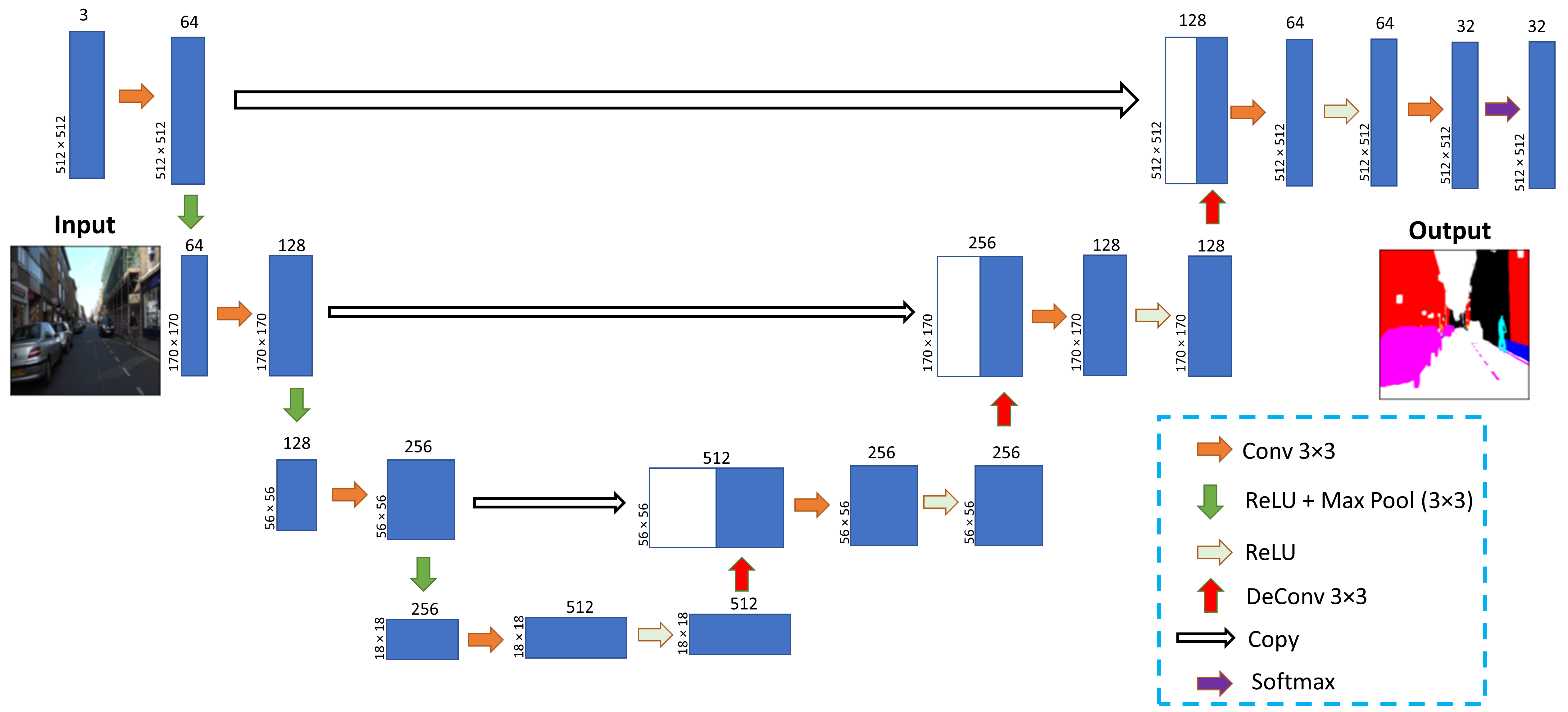
There are multiple architectures developed for image segmentation like UNet, SegNet, etc. Among these, UNet has been widely adopted in segmentation tasks. The UNet architecture was initially proposed by Olaf Ronneberger et al[16] for medical image segmentation. This architecture consists of two main components: the contracting path (also known as the encoder) and the expanding path (also known as the decoder), connected by a copy path (also referred to as skip connection). The contracting path reduces the feature map while extracting image features, and the expanding path utilizes these features to localize objects and reconstruct the segmentation mask[16]. As the feature map undergoes a reduction in the contracting path, some information is lost, to address this, the copy connection (skip connection) is employed to reintroduce the lost information to the expanding path. Figure 1 shows the schematic of a UNet structure, here the contracting path contains convolution, ReLU, and Max-pooling layers while the expanding path contains deconvolution, convolution, and ReLU layers terminated by a softmax function.
Implementing image segmentation through UNet on hardware necessitates the design of circuits dedicated to convolution, deconvolution, ReLU activation functions, and max-pooling layers. In the following sections, we describe the networks designed for these layers.
II.1 Convolution
The convolution operation entails matrix-vector multiplication, where the input is multiplied with a kernel. This matrix-vector multiplication operation is fundamental to artificial neural networks where the input/feature map is multiplied with a weight matrix. In convolution, the kernel can be thought of as a weight matrix. Performing this vector multiplication requires a lot of memory fetches when using traditional hardware based on von-Neumann architecture. So, crossbar arrays[17, 18, 19] have become very popular for matrix-vector multiplication, an example of a crossbar array is shown in Fig. 2. In crossbar arrays, the weight matrix/kernels are stored in non-volatile memory elements (synapses), where analog memory and computing units are intricately interwoven, leading to faster and more energy-efficient matrix multiplication. In Fig. 2, the inputs are applied to horizontal lines, while the kernel weights are stored as conductances of synapses in the vertical lines, and the output of the vector multiplication(weighted sum of inputs) is given by the current value in the vertical lines.
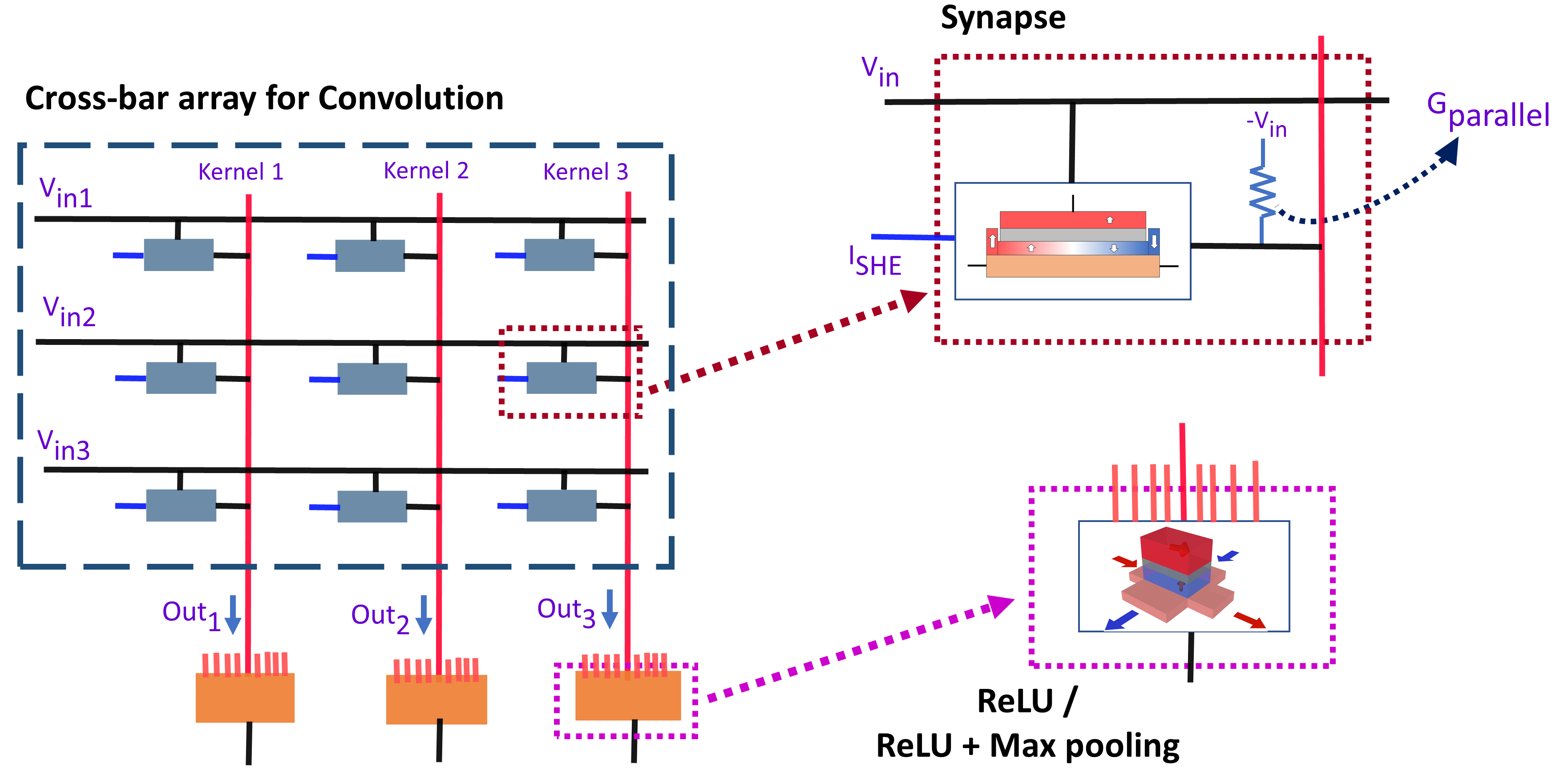
To implement such a crossbar array, a non-volatile synaptic device is necessary. Therefore, we employ a domain-wall-based magnetic tunnel junction (DW-MTJ) device to store the kernel weight. The neural network can have both positive and negative weights, but the conductance values of the DW-MTJ are positive only. To address this we add a conductance in parallel to the DW-MTJ as shown in Fig. 2. So the weight can be represented as
| (1) |
| (2) |
Here, is the weight connecting input with kernel, is the conductance of the DW-MTJ. and are the anti-parallel and parallel concordances of the DW-MTJ. Further details about the DW-MTJ device are elaborated in Section IV.
II.2 Deconvolution
Deconvolution, also referred to as transposed convolution or fractionally-strided convolution, operates in the reverse direction of convolution. It extrapolates new information from the feature map and can be thought of as a one-to-many connection[9]. Deconvolution serves as a technique for upsampling images, resulting in an output size larger than the input size. This operation has significant application in generative adversarial networks and fully convolutional networks[20].
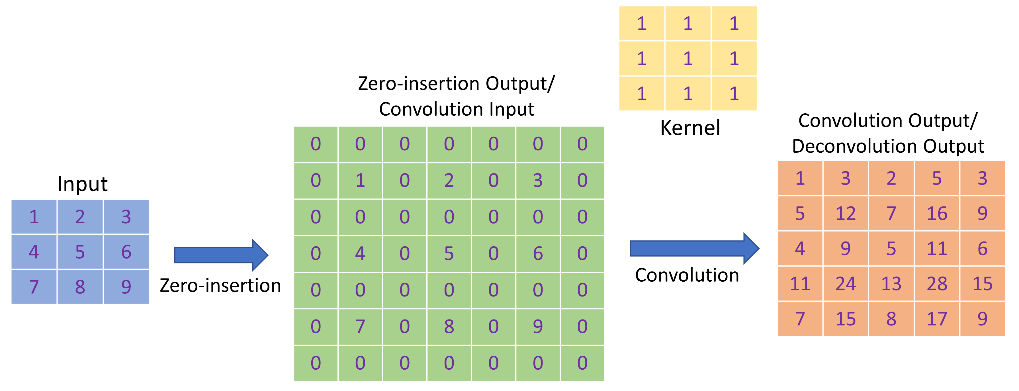
The deconvolution operation can be achieved by introducing zeros into the input matrix and performing a convolution operation[21, 20]. Figure 3 illustrates the deconvolution operation as a combination of zero insertion and convolution. Zeros are inserted along each row and column, including at the edges of the input matrix, thereby expanding the input size. This up-sampled matrix is then used as input for convolution. This combination of zero insertion and convolution yields the same effect as deconvolution. While this method involves redundant operations of multiplication with zeros, it allows us to utilize the convolution operation for which we have designed a hardware implementation using cross-bar arrays in the previous section. This approach reduces the complexity of the hardware design for the segmentation tasks. Hence, in our network design, we represent deconvolution through the convolution operation with an additional step of zero insertion.
II.3 ReLU and Max-pooling
Activation functions play a crucial role in neural networks, introducing non-linearity that enables the network to learn intricate structures and distinguish between outputs[22]. The rectified linear activation function (ReLU)[23] has emerged as a default choice for various networks, as it has been shown to improve learning in neural networks[24, 25, 26]. In convolutional neural networks (CNNs), UNet, and fully connected convolutional networks, a pooling layer is commonly incorporated to reduce the size and parameters while extracting features. Among various pooling methods, max pooling is popular, max pooling also has the ability to suppress noise by discarding noisy activations[22].
To implement the ReLU function, we employ an orthogonal current-injected MTJ design. Subsequently, we utilize this ReLU circuit to construct a max pooling network that simultaneously performs both ReLU and max-pooling functions. We discuss these implementations in Section V.
III Simulation method
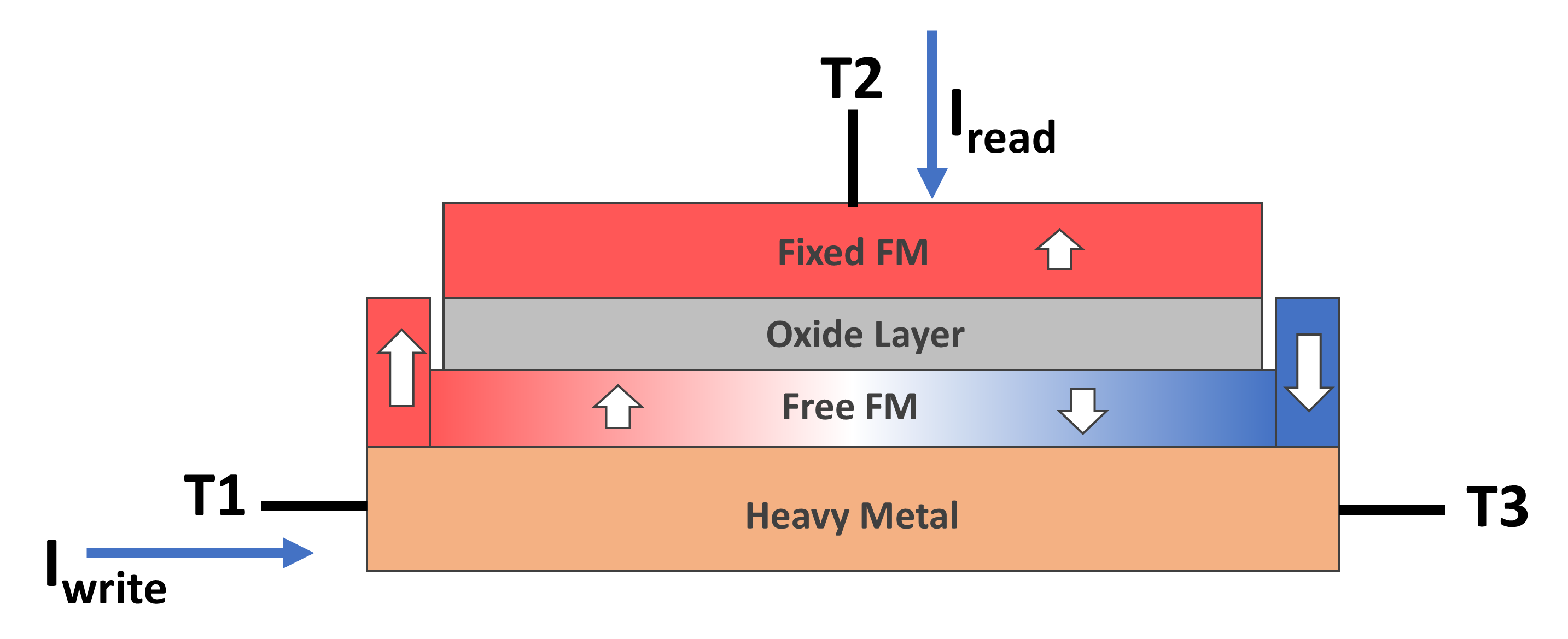
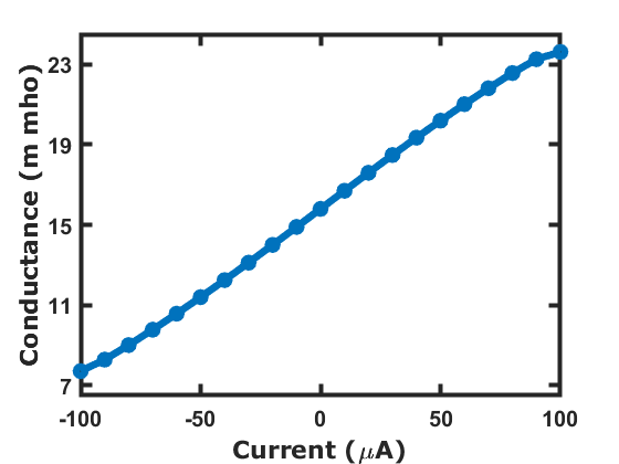
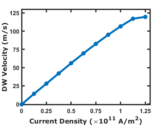
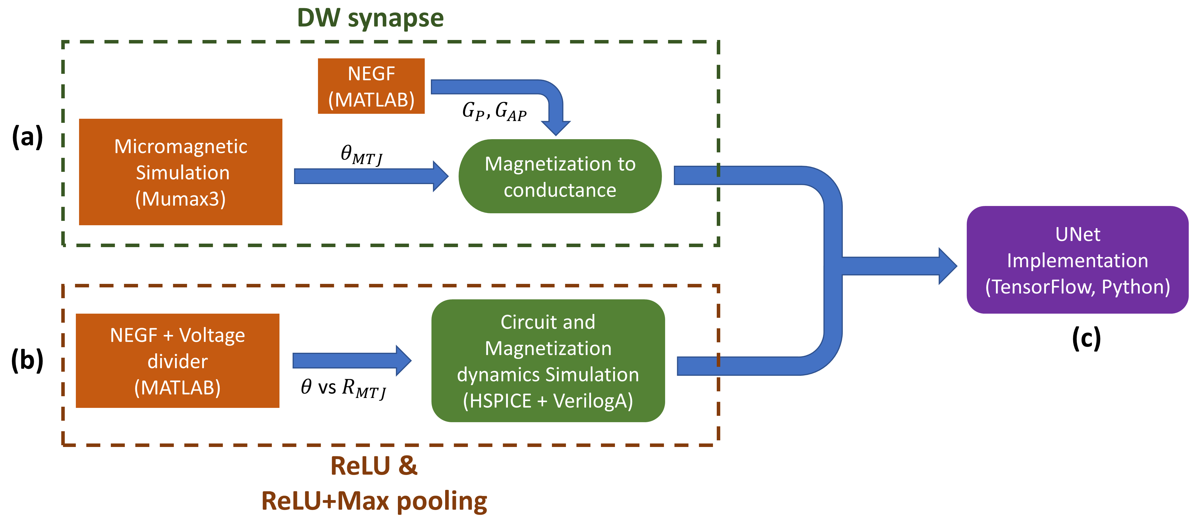
Figure 4 presents an overview of the simulation method, encompassing micromagnetic simulation, NEGF formalism, magnetization dynamics, circuit simulation, and UNet implementation. The simulation can be divided into three components: domain-wall synapse simulation, ReLU-max pooling design, and UNet implementation.
The implementation of the domain-wall synapse involves micromagnetic simulation, which gives the response in magnetization of the free ferromagnetic layer due to applied current. To perform these micromagnetic simulations, the mumax3 software[27, 28] was employed. These magnetization results are used to obtain the conductance of DW-MTJ devices using the following equation [29, 30].
| (3) |
Here, represents the angle between free-FM and fixed-FM magnetizations, and are the parallel and anti-parallel conductances of the MTJ. NEGF simulation is utilized to compute the and conductance values.
In the simulation of the ReLU-Max pooling network, NEGF simulation is self-consistently coupled with the voltage divider(formed by MTJ and a fixed resistor). Here the MTJ angle is varied to find the resistance of the MTJ by iteratively calculating the voltage across the MTJ. The results from the NEGF simulation are incorporated into the HSPICE circuit simulator through VerilogA. The HSPICE also performs magnetization dynamics simulation to find the MTJ angle along with the CMOS device simulations based on the 16nm predictive technology model[31]. The results of the domain-wall synapse, ReLU, and max pooling are incorporated into the Python programming, where the UNet architecture shown in Fig.1 is implemented using the TensorFlow package.
III.1 Quantum transport: NEGF
We use the Keldysh NEGF technique [32, 33, 12] to simulate the transport through MTJ that has MgO sandwiched between free and fixed CoFeB FM layers. The NEGF formalism is given by
| (4) | |||
| (5) | |||
| (6) | |||
| (7) |
Here is the Green’s function matrix, is the identity matrix, is the energy variable, is the device Hamiltonian, is the device tight-binding matrix, is the Coulomb charging matrix, is the self-energy matrix and are the self-energy matrices for the top (fixed) and bottom (free) FM layers respectively. is the electron correlation matrix and is the in-scattering function.
The quantum transport part leads to the calculation of the current operator () that represents the charge current between two lattice points i and i+1 is given by
| (8) |
| (9) |
The current operator is matrix in the spin space of the lattice point. Here is the charge current through the MTJ device and is the quantum of electronic charge.
III.2 Magnetization dynamics
The LLGS equation [34, 35] is used to describe the magnetization dynamics of the free-FM. The LLGS equation is given by
| (10) |
where is the unit vector along the direction of magnetization of the free magnet, is the gyromagnetic ratio, is the Gilbert damping parameter, is the reduced effective field and is the normalized spin current. The term includes the contribution of the anisotropy field () and the thermal noise (). The thermal noise[36] is given by and represents the ensemble average.
III.3 SHE layer
The charge-to-spin conversion via the spin hall effect(SHE) in heavy metals is used to effectively manipulate the free-FM magnetization. The charge-to-spin conversion of the SHE layer and the polarization of the generated current is given by [37, 38, 39]
| (11) |
| (12) |
| (13) |
Here, is the spin current density and is the charge current density. is the spin current generated, is the spin Hall angle of the heavy metal, L, t are the length and thickness of the heavy metal, and is the charge current injected. is the direction of generated spin current flow, is the direction of input charge current, and is the polarization of the generated spin current. From Eq. 13, injection of charge current to heavy metal in direction results in y-polarized spin current injection to the free-FM (z-direction) on top of the HM layer.
The resistance (R) of the heavy metal is given by
| (14) |
Here, and W are the resistivity and width of the heavy metal respectively.
IV Domain wall Synapse
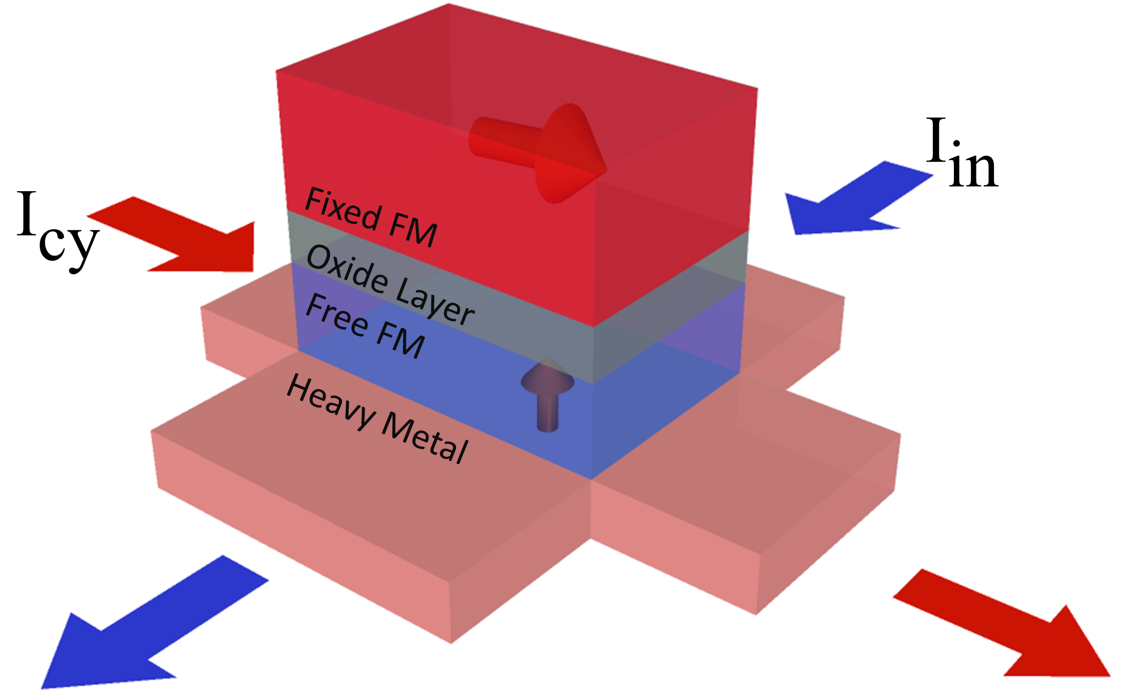
The domain wall synapse is a 3-terminal device as shown in Fig. 5. In this 3-terminal configuration, the read and write paths are distinct, preventing accidental modification of synapse information during reading[29, 30]. The write path in the DW device, illustrated in Fig. 5, is between terminals T1 and T3, while the read path is between terminals T2 and T3. The free-FM layer of the DW-MTJ has two oppositely polarized magnetic regions separated by a domain wall. This domain wall can be moved by spin orbit torque (SOT) exerted by the heavy metal. Thus the charge current flowing through the heavy metal injects spin current into the free-FM layer and moves the domain wall. The two pinned layers on either side of the free FM layer help prevent the domain wall from getting destroyed when a high current is applied. The movement of the domain wall causes one magnetic region to shrink while the other expands this changes the average magnetization of the free-FM layer. This change in magnetization translates to a variation in the conductance of the device, due to the tunnel magneto-resistance effect of the MTJ.
IV.1 Device parameters
The spin orbit coupling at the heavy metal-free FM interface leads to Dzyaloshinskii-Moriya exchange interaction (DMI) which stabilizes the Neel Domain wall[40, 41, 42, 29, 30]. For our synaptic device, we consider a PMA CoFeB ferromagnet with dimensions , saturation magnetization() of 0.7 , PMA constant() of 0.8 , exchange-correlation constant() of 10 , damping constant() of 0.3 and DMI constant() of 1.2 . We consider the highly efficient heavy metal [43, 44], with spin hall angle () of 0.3, resistivity () of 83 and a thickness of 4nm, resulting in a resistance of 1037.5 . is taken as a heavy metal since it has a low spin Hall power factor[44] so it is more power efficient compared to other heavy metals.
IV.2 Results
We show in Fig. 5 the linear conductance relation of the DW-MTJ with the input write current pulse. The domain wall’s initial position is at the center, and a current pulse of 2ns duration is applied. We observed that a 100 current pulse is needed to move the domain wall to the right edge starting from the center, corresponding to the parallel alignment with the fixed FM layer, and -100 is needed to move the domain wall to the left edge, corresponding to the anti-parallel alignment with the fixed FM layer. The velocity of the domain wall due to applied current is shown in Fig. 5, which shows a linear relation for the considered parameters.
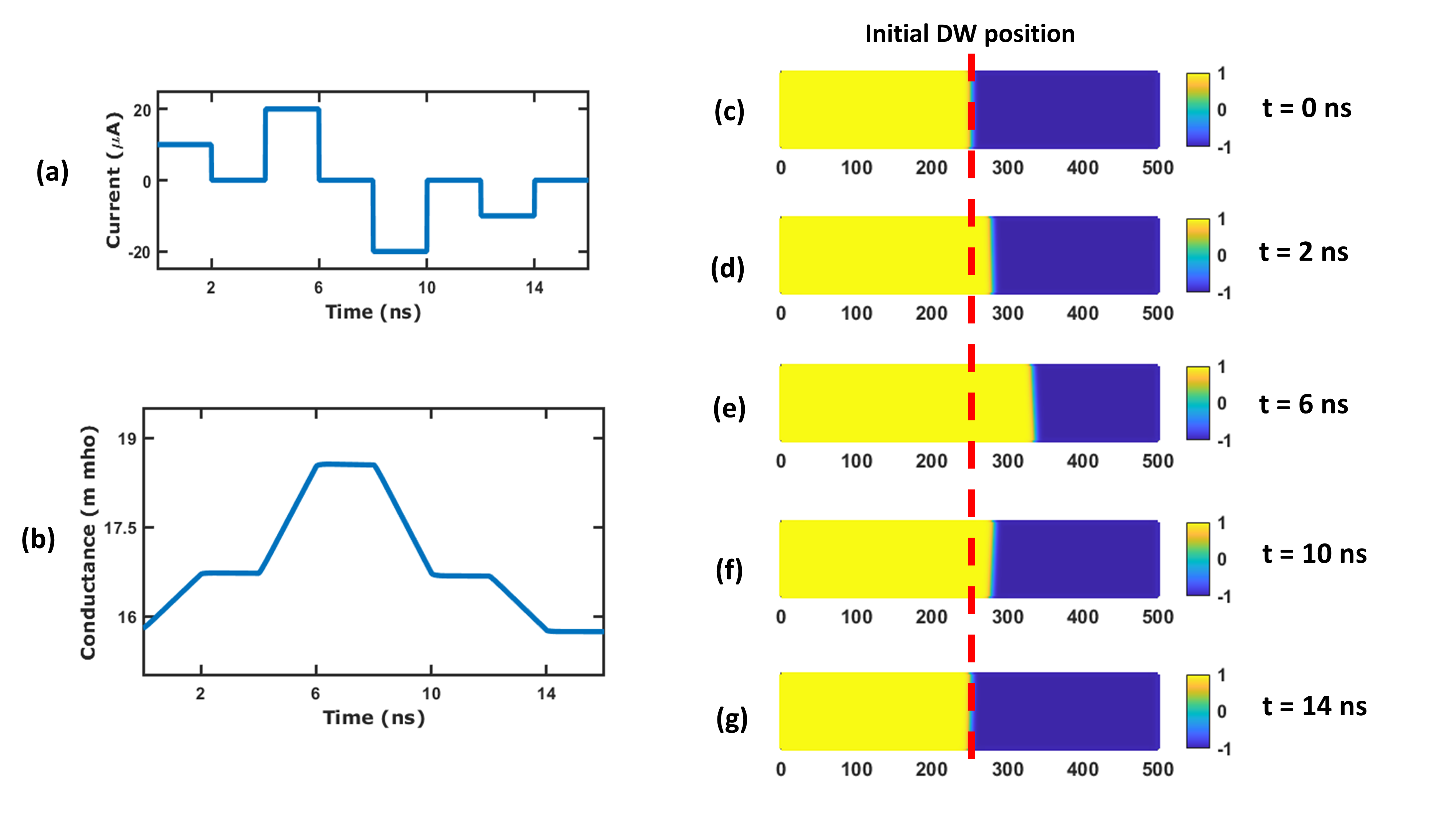
During the training of the neural network, the weights increase and decrease, so corresponding to this requirement we show in Fig. 6 the response of the DW-MTJ to an input write current pulse train. Figure 6(a) shows the current pulse train, and the corresponding conductance of the DW-MTJ is shown in 6(b) over time. Figure. 6(c) - (g) show the snapshots of the free-FM magnetization showing the movement of the domain wall. We observe that the domain wall reaches its initial position over time as the net current applied is zero. We also noted the tilting of the domain wall in the presence of current, this can be explained through 1D domain wall theory[41].
V ReLU and Max pooling
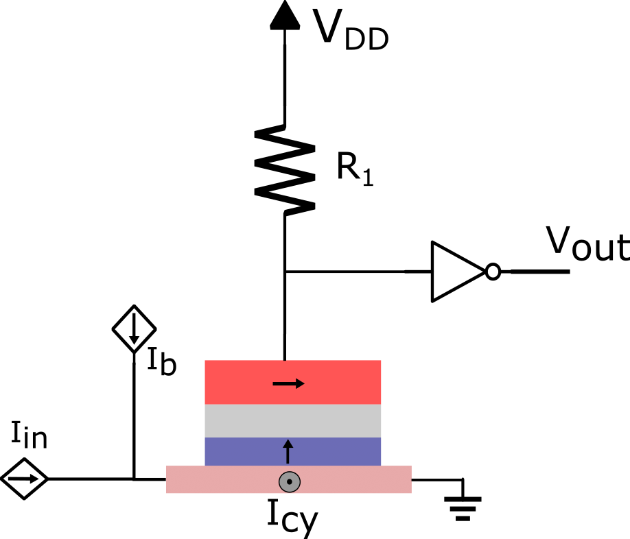
The magnetic tunnel junction possesses several properties, including the ability to undergo continuous/linear changes in resistance, which can be achieved by applying orthogonal spin currents to the free-FM of the MTJ [11]. This continuous change in resistance is essential since the ReLU function contains linear regions, requiring a device with linear characteristics for its emulation. Figure 7 illustrates the schematic of the MTJ injected with orthogonal spin currents generated by the SHE layer. This linear behavior of the MTJ can be utilized to construct a circuit that emulates the ReLU function, as depicted in Fig. 7. The circuit incorporates a resistor , a CMOS inverter, and the MTJ device along with a current source to shift the output and generate the ReLU function.
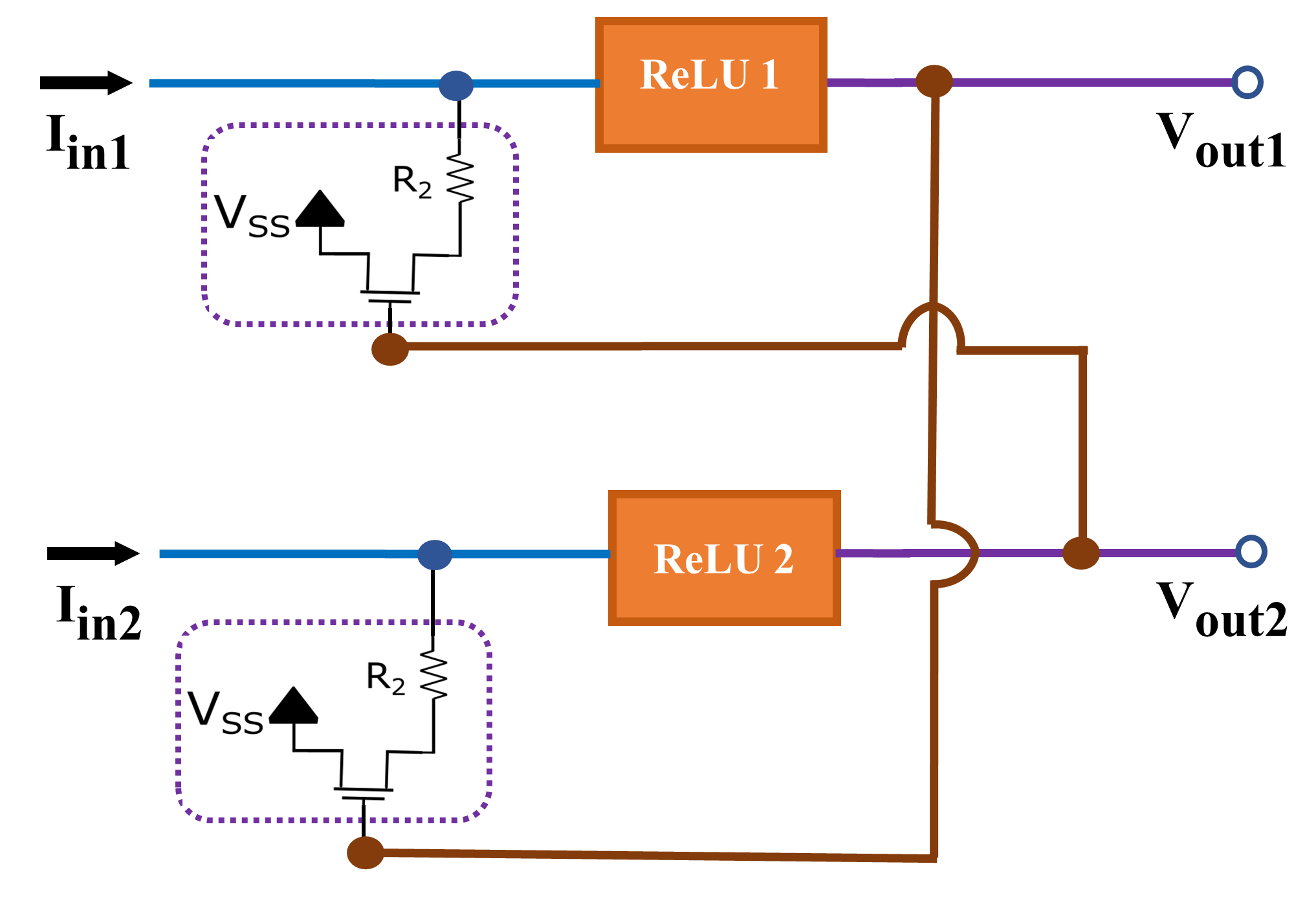
The max pooling function entails finding the maximum of the presented inputs. To achieve this functionality we use multiple ReLU circuits and introduce competition among them so that the circuit with the highest input becomes the winner. We enable this competition through an n-MOSFET and a resistor connected between each pair of ReLU circuits as shown in Fig. 8.
V.1 Device parameters
For the ReLU-max pooling circuits, we utilize a PMA CoFeB ferromagnet with dimensions 14.469.41nm. The saturation magnetization () is 1150, anisotropy field () is 330Oe, the Gilbert damping is 0.01, the thermal stability factor () is 4.58, a lower thermal stability factor was used as it reduces the power consumption and our circuit design still gives accurate results [11, 23]. The heavy metal used is [43, 44], with spin hall angle () of 0.3, resistivity () of 83 and a thickness of 4nm, resulting in input resistance of 1000. The circuit parameters, the current bias is 9.98, resistor is 698.93k and the resistor is 16k.
V.2 Results
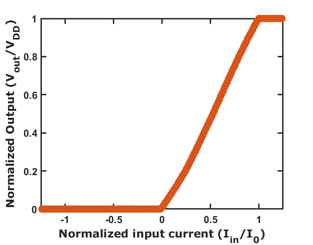
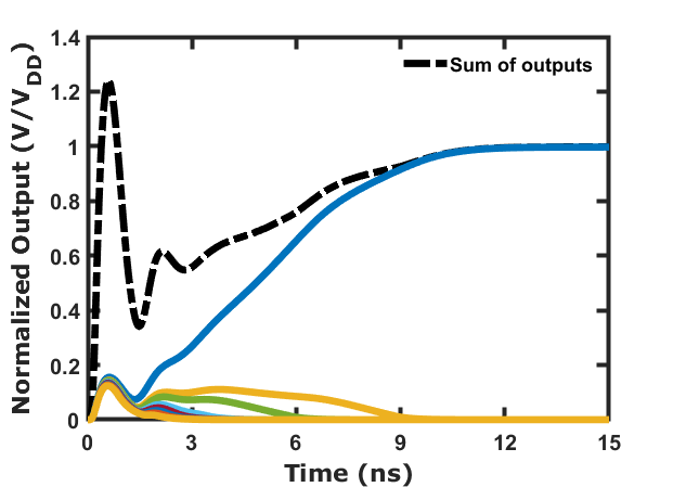
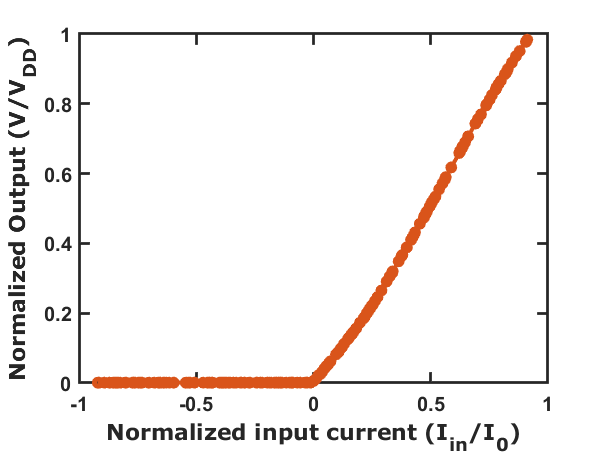
Figure 7 shows the output of the ReLU circuit, which closely resembles the ReLU activation function for normalized inputs of less than 1, here the normalized current is 14.5. The ReLU circuit consumes an average power of 0.343. We show in Fig. 8 the transient results of the ReLU-Max pooling circuit, the 9 inputs are randomly taken to show max pooling functionality. Here we observe competition among the 9 ReLU circuits that enable the max pooling functionality, where the ReLU circuit with the highest input reaches its corresponding output while pushing all other ReLU units to settle to 0V. Figure 8 shows the output of the ReLU-max pooling network where the inputs are chosen using the Monte Carlo simulation. This output closely resembles the ReLU function, demonstrating that our network performs both max pooling and ReLU functions simultaneously. The ReLU-max pooling network consumes an average power of 17.86.
VI Segmentation results
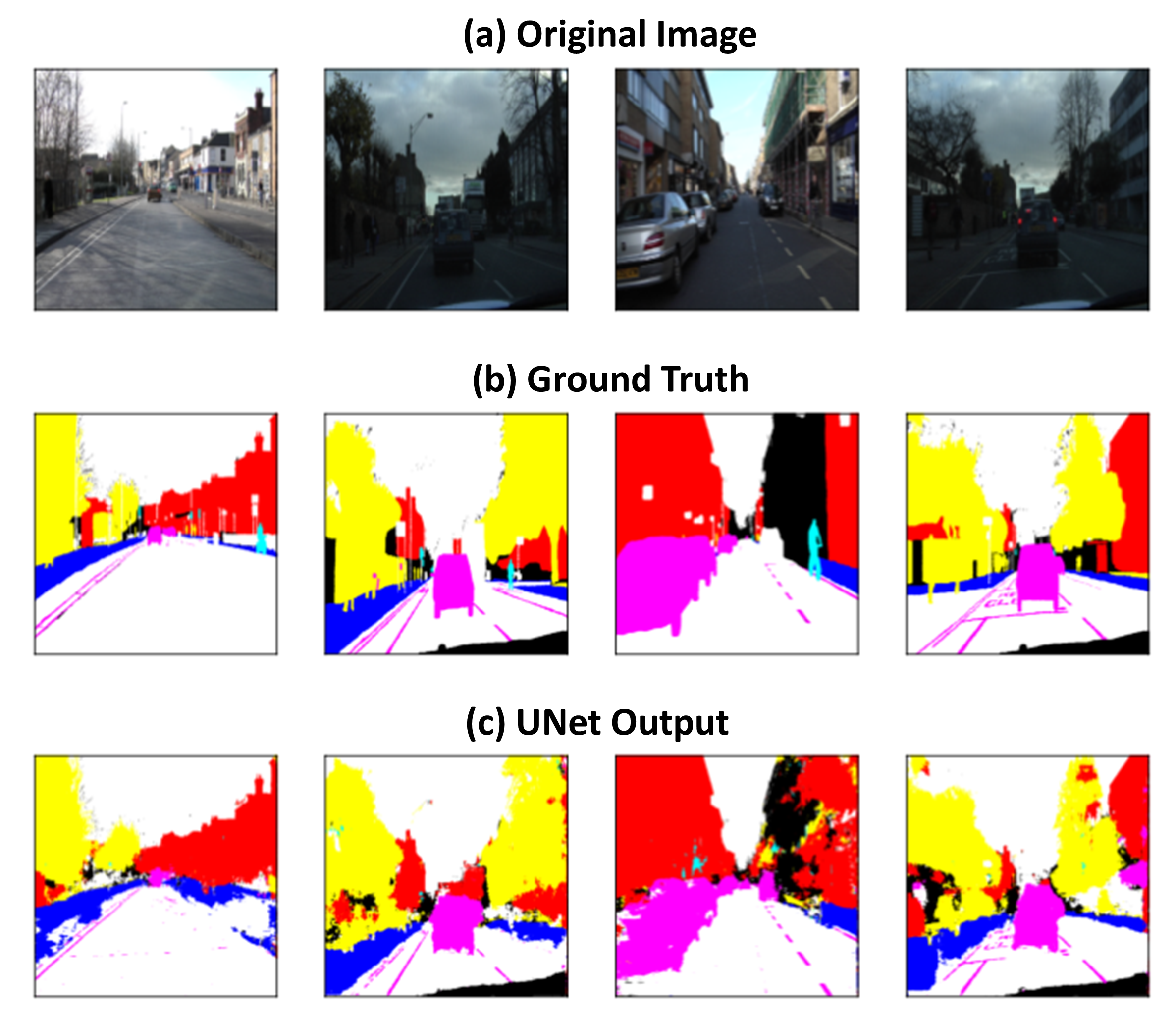
We evaluate our UNet design using the Cambridge-driving labeled video (CamVid) Database [45]. This data was captured from the perspective of a driving car, the driving scene increases the number and diversity of the observed object classes. The dataset contains 701 colored images with dimensions of pixels, each pixel is labeled into one of 32 possible classes. These classes include objects such as buildings, cars, roads, children, bicyclists, etc. To evaluate our network, we partitioned the 701 images into sets of 369 for training, 100 for validation, and 232 for testing purposes.
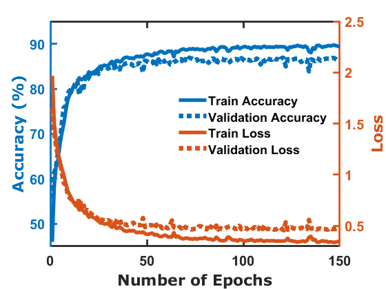
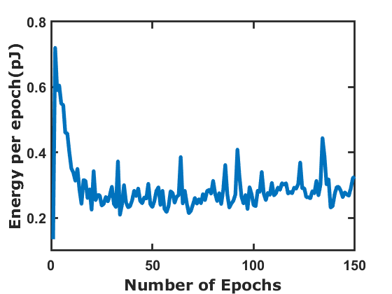
Figure 9 shows the accuracy() and loss of UNet over 150 epochs for testing and validation datasets. We achieved a validation accuracy of 86.48 and testing accuracy of 82.34, these results closely resemble those of the fully software-based implementation, where the validation accuracy is 87.95 and the testing accuracy is 84.53. We also calculated the energy consumed by the synapses during training as shown in Fig. 9. The energy dissipation per epoch decreases as the network undergoes training and the weights converge. The total energy consumed by all the synapses during training over 150 epochs is 43.59.
We show in Fig. 10 the UNet output of four test images along with the ground truth labels. Here the predicted segmentation results based on our spintronic hardware implementation of UNet closely resemble the ground truth labels.
VII Conclusion
In this article, we proposed hardware implementation for highly complex image segmentation tasks. We demonstrated the synaptic behavior of domain wall MTJ and constructed the convolution operation using the domain wall-based cross-bar array. We showed that deconvolution can be implemented using the same hardware design as convolution. Using the linear behavior of MTJ through orthogonal current injection, we showcased the implementation of ReLU and max pooling functions. We presented our simulation platform where we couple the micromagnetic simulation, NEGF, circuit simulation, and Python programming to capture the diverse physics of spin-transport, magnetization dynamics, and CMOS elements. We demonstrated the potential of our hardware implementation of UNet by assessing its performance on the CamVid dataset. Our results closely match those obtained from software implementation, while consuming 43.59pJ of energy for weight updates during training.
Acknowledgments
The author BM acknowledges the support by the Science and Engineering Research Board (SERB), Government of India, Grant No. MTR/2021/000388, and the Ministry of Human Resource Development (MHRD), Government of India, Grant No. STARS/APR2019/NS/226/FS under the STARS scheme. The author AS acknowledges the support by SERB, Grant No. SRG/2023/001327.
References
- [1] Thanos Athanasiadis, Phivos Mylonas, Yannis Avrithis, and Stefanos Kollias. Semantic image segmentation and object labeling. IEEE transactions on circuits and systems for video technology, 17(3):298–312, 2007.
- [2] Xiaolong Liu, Zhidong Deng, and Yuhan Yang. Recent progress in semantic image segmentation. Artificial Intelligence Review, 52:1089–1106, 2019.
- [3] Martin Thoma. A survey of semantic segmentation. arXiv preprint arXiv:1602.06541, 2016.
- [4] Saeid Asgari Taghanaki, Kumar Abhishek, Joseph Paul Cohen, Julien Cohen-Adad, and Ghassan Hamarneh. Deep semantic segmentation of natural and medical images: a review. Artificial Intelligence Review, 54:137–178, 2021.
- [5] Yaodong Cui, Ren Chen, Wenbo Chu, Long Chen, Daxin Tian, Ying Li, and Dongpu Cao. Deep learning for image and point cloud fusion in autonomous driving: A review. IEEE Transactions on Intelligent Transportation Systems, 23(2):722–739, 2021.
- [6] Chengquan Huang, LS Davis, and JRG Townshend. An assessment of support vector machines for land cover classification. International Journal of remote sensing, 23(4):725–749, 2002.
- [7] Julie Grollier, Damien Querlioz, KY Camsari, Karin Everschor-Sitte, Shunsuke Fukami, and Mark D Stiles. Neuromorphic spintronics. Nature electronics, 3(7):360–370, 2020.
- [8] Radhika V Menon, Shantharam Kalipatnapu, and Indrajit Chakrabarti. High speed vlsi architecture for improved region based active contour segmentation technique. Integration, 77:25–37, 2021.
- [9] Shuanglong Liu, Hongxiang Fan, Xinyu Niu, Ho-cheung Ng, Yang Chu, and Wayne Luk. Optimizing cnn-based segmentation with deeply customized convolutional and deconvolutional architectures on fpga. ACM Transactions on Reconfigurable Technology and Systems (TRETS), 11(3):1–22, 2018.
- [10] S-W Chung, Tatsuya Kishi, Jung Woo Park, Masatoshi Yoshikawa, Kyung-Seok Park, Toshihiko Nagase, K Sunouchi, H Kanaya, GC Kim, K Noma, et al. 4gbit density stt-mram using perpendicular mtj realized with compact cell structure. In 2016 IEEE International Electron Devices Meeting (IEDM), pages 27–1. IEEE, 2016.
- [11] Venkatesh Vadde, Bhaskaran Muralidharan, and Abhishek Sharma. Orthogonal spin current injected magnetic tunnel junction for convolutional neural networks. IEEE Transactions on Electron Devices, 70(7):3943–3950, 2023.
- [12] Abhishek Sharma, Ashwin A Tulapurkar, and Bhaskaran Muralidharan. Resonant spin-transfer-torque nano-oscillators. Physical Review Applied, 8(6):064014, 2017.
- [13] Atsufumi Hirohata, Keisuke Yamada, Yoshinobu Nakatani, Ioan-Lucian Prejbeanu, Bernard Diény, Philipp Pirro, and Burkard Hillebrands. Review on spintronics: Principles and device applications. Journal of Magnetism and Magnetic Materials, 509:166711, 2020.
- [14] Kerem Yunus Camsari, Sayeef Salahuddin, and Supriyo Datta. Implementing p-bits with embedded mtj. IEEE Electron Device Letters, 38(12):1767–1770, 2017.
- [15] Partha Kaushik, Amit Monga, Hemkant Nehete, and Brajesh Kumar Kaushik. Enhancing image segmentation performance with mram based processing-in-memory architecture. In 2023 IEEE Nanotechnology Materials and Devices Conference (NMDC), pages 836–841. IEEE, 2023.
- [16] Olaf Ronneberger, Philipp Fischer, and Thomas Brox. U-net: Convolutional networks for biomedical image segmentation. In Medical Image Computing and Computer-Assisted Intervention–MICCAI 2015: 18th International Conference, Munich, Germany, October 5-9, 2015, Proceedings, Part III 18, pages 234–241. Springer, 2015.
- [17] Qiangfei Xia and J Joshua Yang. Memristive crossbar arrays for brain-inspired computing. Nature materials, 18(4):309–323, 2019.
- [18] Seungchul Jung, Hyungwoo Lee, Sungmeen Myung, Hyunsoo Kim, Seung Keun Yoon, Soon-Wan Kwon, Yongmin Ju, Minje Kim, Wooseok Yi, Shinhee Han, et al. A crossbar array of magnetoresistive memory devices for in-memory computing. Nature, 601(7892):211–216, 2022.
- [19] Varun Bhavin Desai, Divya Kaushik, Janak Sharda, and Debanjan Bhowmik. On-chip learning of a domain-wall-synapse-crossbar-array-based convolutional neural network. Neuromorphic Computing and Engineering, 2(2):024006, 2022.
- [20] Ziru Li, Bing Li, Zichen Fan, and Hai Li. Red: A reram-based efficient accelerator for deconvolutional computation. IEEE Transactions on Computer-Aided Design of Integrated Circuits and Systems, 39(12):4736–4747, 2020.
- [21] Fan Chen, Linghao Song, and Yiran Chen. Regan: A pipelined reram-based accelerator for generative adversarial networks. In 2018 23rd Asia and South Pacific Design Automation Conference (ASP-DAC), pages 178–183. IEEE, 2018.
- [22] Ian Goodfellow, Yoshua Bengio, and Aaron Courville. Deep learning. MIT press, 2016.
- [23] Venkatesh Vadde, Bhaskaran Muralidharan, and Abhishek Sharma. She-mtj based relu-max pooling functions for on-chip training of neural networks. AIP Advances, 14(2):025130, 2024.
- [24] Xavier Glorot, Antoine Bordes, and Yoshua Bengio. Deep sparse rectifier neural networks. In Proceedings of the fourteenth international conference on artificial intelligence and statistics, pages 315–323. JMLR Workshop and Conference Proceedings, 2011.
- [25] Hidenori Ide and Takio Kurita. Improvement of learning for cnn with relu activation by sparse regularization. In 2017 international joint conference on neural networks (IJCNN), pages 2684–2691. IEEE, 2017.
- [26] Vinod Nair and Geoffrey E Hinton. Rectified linear units improve restricted boltzmann machines. In Proceedings of the 27th international conference on machine learning (ICML-10), pages 807–814, 2010.
- [27] Arne Vansteenkiste, Jonathan Leliaert, Mykola Dvornik, Mathias Helsen, Felipe Garcia-Sanchez, and Bartel Van Waeyenberge. The design and verification of mumax3. AIP advances, 4(10), 2014.
- [28] Jeroen Mulkers, Bartel Van Waeyenberge, and Milorad V Milošević. Effects of spatially engineered dzyaloshinskii-moriya interaction in ferromagnetic films. Physical Review B, 95(14):144401, 2017.
- [29] Abhronil Sengupta, Yong Shim, and Kaushik Roy. Proposal for an all-spin artificial neural network: Emulating neural and synaptic functionalities through domain wall motion in ferromagnets. IEEE transactions on biomedical circuits and systems, 10(6):1152–1160, 2016.
- [30] Debanjan Bhowmik, Utkarsh Saxena, Apoorv Dankar, Anand Verma, Divya Kaushik, Shouri Chatterjee, and Utkarsh Singh. On-chip learning for domain wall synapse based fully connected neural network. Journal of Magnetism and Magnetic Materials, 489:165434, 2019.
- [31] Predictive technology model (ptm). https://ptm.asu.edu/.
- [32] Kerem Y Camsari, Shuvro Chowdhury, and Supriyo Datta. The non-equilibrium green function (negf) method. arXiv preprint arXiv:2008.01275, 2020.
- [33] Deepanjan Datta, Behtash Behin-Aein, Supriyo Datta, and Sayeef Salahuddin. Voltage asymmetry of spin-transfer torques. IEEE Transactions on Nanotechnology, 11(2):261–272, 2011.
- [34] John C Slonczewski. Current-driven excitation of magnetic multilayers. Journal of Magnetism and Magnetic Materials, 159(1-2):L1–L7, 1996.
- [35] Georgios D Panagopoulos, Charles Augustine, and Kaushik Roy. Physics-based spice-compatible compact model for simulating hybrid mtj/cmos circuits. IEEE Transactions on Electron Devices, 60(9):2808–2814, 2013.
- [36] Jonathan Z Sun, TS Kuan, JA Katine, and Roger H Koch. Spin angular momentum transfer in a current-perpendicular spin-valve nanomagnet. In Quantum Sensing and Nanophotonic Devices, volume 5359, pages 445–455. SPIE, 2004.
- [37] Cheng Song, Ruiqi Zhang, Liyang Liao, Yongjian Zhou, Xiaofeng Zhou, Ruyi Chen, Yunfeng You, Xianzhe Chen, and Feng Pan. Spin-orbit torques: Materials, mechanisms, performances, and potential applications. Progress in Materials Science, 118:100761, 2021.
- [38] Luqiao Liu, OJ Lee, TJ Gudmundsen, DC Ralph, and RA Buhrman. Current-induced switching of perpendicularly magnetized magnetic layers using spin torque from the spin hall effect. Physical review letters, 109(9):096602, 2012.
- [39] Saburo Takahashi and Sadamichi Maekawa. Spin current, spin accumulation and spin hall effect. Science and Technology of Advanced Materials, 9(1):014105, 2008.
- [40] Satoru Emori, Uwe Bauer, Sung-Min Ahn, Eduardo Martinez, and Geoffrey SD Beach. Current-driven dynamics of chiral ferromagnetic domain walls. Nature materials, 12(7):611–616, 2013.
- [41] Eduardo Martinez, Satoru Emori, Noel Perez, Luis Torres, and Geoffrey SD Beach. Current-driven dynamics of dzyaloshinskii domain walls in the presence of in-plane fields: Full micromagnetic and one-dimensional analysis. Journal of Applied Physics, 115(21), 2014.
- [42] Kowsar Shahbazi, Aleš Hrabec, Simone Moretti, Michael B Ward, Thomas A Moore, Vincent Jeudy, Eduardo Martinez, and Christopher H Marrows. Magnetic properties and field-driven dynamics of chiral domain walls in epitaxial pt/co/au x pt 1- x trilayers. Physical Review B, 98(21):214413, 2018.
- [43] Lijun Zhu, Daniel C Ralph, and Robert A Buhrman. Highly efficient spin-current generation by the spin hall effect in au 1- x pt x. Physical Review Applied, 10(3):031001, 2018.
- [44] Venkatesh Vadde, Bhaskaran Muralidharan, and Abhishek Sharma. Power efficient relu design for neuromorphic computing using spin hall effect. Journal of Physics D: Applied Physics, 56(41):415001, 2023.
- [45] Gabriel J Brostow, Julien Fauqueur, and Roberto Cipolla. Semantic object classes in video: A high-definition ground truth database. Pattern Recognition Letters, 30(2):88–97, 2009.