A chip-integrated comb-based microwave oscillator
Low-noise microwave oscillators are cornerstones for wireless communication, radar and clocks. The employment and optimization of optical frequency combs have enabled photonic microwave synthesizers with unrivalled noise performance and bandwidth breaking the bottleneck of those electronic counterparts Fortier et al. (2011); Xie et al. (2016); Li et al. (2014); Nakamura et al. (2020). Emerging interest has been concentrated on photonic microwave generation using chip-based Kerr frequency combs, namely microcombs Kippenberg et al. (2018); Pasquazi et al. (2018). Today microcombs built on photonic integrated circuits feature small size, weight and power consumption Moss et al. (2013); Gaeta et al. (2019); Liu et al. (2021), and can be designed and manufactured to oscillate at any target frequency ranging from microwave to millimeter-wave band Liang et al. (2015a); Liu et al. (2020a); Yao et al. (2022); Tetsumoto et al. (2021); Wang et al. (2021). However, a monolithic microcomb-based microwave oscillator requires photonic integration of lasers, photodetectors and nonlinear microresonators on a common substrate, which has still remained elusive. Here, we demonstrate the first of such a fully integrated, microcomb-based, photonic microwave oscillator at 10.7 GHz. The chip device, powered by a customized microelectronic circuit, leverages hybrid integration of a high-power DFB laser, a Si3N4 microresonator of a quality factor exceeding 25106, and a high-speed photodetector chip of 110 GHz bandwidth (3-dB) and 0.3 A/W responsivity. Each component represents the state of the art of its own class, yet also allows large-volume manufacturing with low cost using established CMOS foundries. The hybrid chip outputs an ultralow-noise laser of 6.9 Hz intrinsic linewidth, a coherent microcomb of 10.7 GHz repetition rate, and a 10.7 GHz microwave carrier of 6.3 mHz linewidth – all the three functions in one entity occupying a footprint of only 76 mm2. The microwave phase noise reaches 75/105/130 dBc/Hz at 1/10/100 kHz Fourier offset frequency. Our results can reinvigorate our information society for communication, sensing, imaging, timing and precision measurement.
Introduction. Low-noise microwave oscillators are ubiquitously deployed in our information society for communication, sensing, spectroscopy and timing. A particularly important frequency band is the microwave X-band (8 to 12 GHz), dedicated for radar, wireless networks, and satellite communication. Currently, a paradigm shift is ongoing which utilizes photonics to synthesize X-band microwaves Fortier et al. (2011); Xie et al. (2016); Li et al. (2014); Liang et al. (2015a); Liu et al. (2020a); Yao et al. (2022); Li et al. (2013a); Li and Vahala (2023); Tang et al. (2018). Compared to the electronic counterpart, the photonic microwave generation enables unrivalled performance, particularly in noise and bandwidth.
Among all photonics-based approaches, optical frequency combs Cundiff and Ye (2003); Fortier and Baumann (2019); Diddams et al. (2020), which coherently link radio- or microwave frequency to optical frequency, have enabled microwaves with unrivalled spectral purity (noise) by leveraging optical frequency division (OFD) Fortier et al. (2011); Xie et al. (2016); Li et al. (2014). Optical-clock-referenced OFD Nakamura et al. (2020) has created 10 GHz microwaves with fractional frequency instability at 1 s, two orders of magnitude more stable than the cesium fountain clocks defining the SI second. Currently, by virtue of high- optical microresonators and harnessing the Kerr nonlinearity, an emerging paradigm is to develop and apply microresonator-based Kerr frequency combs, i.e. “microcombs” Kippenberg et al. (2018); Pasquazi et al. (2018); Herr et al. (2013); Yi et al. (2015); Brasch et al. (2016); Joshi et al. (2016); Xue et al. (2015) that have small size, weight and power consumption. In particular, exploiting recent breakthroughs in fabrication of ultralow-loss photonic integrated circuits (PIC) Moss et al. (2013); Gaeta et al. (2019); Liu et al. (2021), optical microresonators can now be constructed on a plethora of integrated material platforms Kovach et al. (2020); Chang et al. (2022). These PIC-based microresonators have permitted chip-level microcombs with diverse merits and functions. Notably, latest endeavors have demonstrated microcomb-based OFD Kudelin et al. (2023); Sun et al. (2023); Jin et al. (2024); He et al. (2024). Despite, these OFD setups are still bulky, and require sophisticated locking techniques and external references. Therefore, a free-running microcomb-based microwave oscillator that is fully integrated at chip scale is still beneficial, though the phase noise can be compromised.
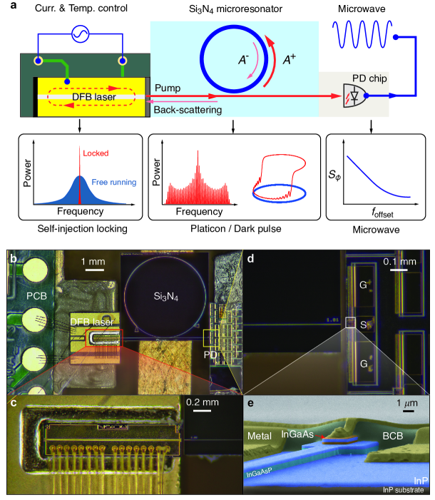
Here, we demonstrate the first fully integrated, microcomb-based, photonic microwave oscillator. The chip device leverages hybrid integration Stern et al. (2018); Raja et al. (2019); Shen et al. (2020) of a distributed-feedback (DFB) laser chip, a high- silicon nitride (Si3N4) microresonator chip, and a photodetector (PD) chip. The schematic and components are depicted in Fig. 1. The DFB laser chip is driven and stabilized by a microelectronic circuit, and emits CW light at 1550 nm. Via edge-coupling, the light enters the Si3N4 microresonator of 10.7 GHz free spectral range (FSR), where a coherent platicon microcomb of 10.7 GHz repetition rate is formed. The output light from the Si3N4 microresonator is delivered to the PD chip. Upon photodetection of the microcomb’s repetition rate Liang et al. (2015a); Liu et al. (2020a); Yao et al. (2022), the PD outputs a microwave carrier of 10.7 GHz and its harmonics. The entire device occupies a footprint of only 76 mm2.
Characterization of individual components
Laser. We use a commercial DFB laser as shown in Fig. 1b,c. The laser outputs 160 mW CW light at 1549.9 nm with 500 mA laser current. The free-running DFB laser exhibits 55 mA current at laser threshold, transverse-electric (TE) polarization, and 1 nm wavelength tunability over a laser current up to 500 mA. The laser’s temperature is stabilized at 30∘C using a thermo-electric cooler (TEC). A printed circuit board (PCB) provides driving current and temperature stabilization to the laser chip. The laser chip is edge-coupled to the Si3N4 chip Raja et al. (2019); Shen et al. (2020); Lihachev et al. (2022). The laser output waveguide is aligned to the inverse taper of the Si3N4 bus waveguide and side-coupled to the microresonator. The coupling efficiency between the laser chip and the Si3N4 chip is measured as 23%, i.e. with 6.4 dB insertion loss. Extra characterization data are shown in Supplementary Information. This loss value can be reduced in the future using optimized inverse taper that matches the laser output mode.
Microresonator. The Si3N4 chip contains a high- microresonator of 10.7 GHz FSR, as shown in Fig. 1b. A high is critical for microcomb generation, since the power threshold for Kerr parametric oscillation is , where is the FSR Kippenberg et al. (2018); Pasquazi et al. (2018). We fabricate Si3N4 waveguides of 300 nm thickness using a deep-ultraviolet (DUV) subtractive process on 150-mm-diameter (6-inch) wafers Ye et al. (2023). The optimized fabrication process is described in Supplementary Information. We choose 300 nm Si3N4 thickness for the following reasons. First, since high-quality Si3N4 films deposited via low-pressure chemical vapor deposition (LPCVD, as used in our case) are prone to crack due to intrinsic tensile stress Luke et al. (2013), Si3N4 films with thickness below 300 nm are free from cracks. Second, 300-nm-thick Si3N4 fabrication process is currently established as a standard process in nearly all CMOS foundries worldwide Muñoz et al. (2019); Xiang et al. (2022).
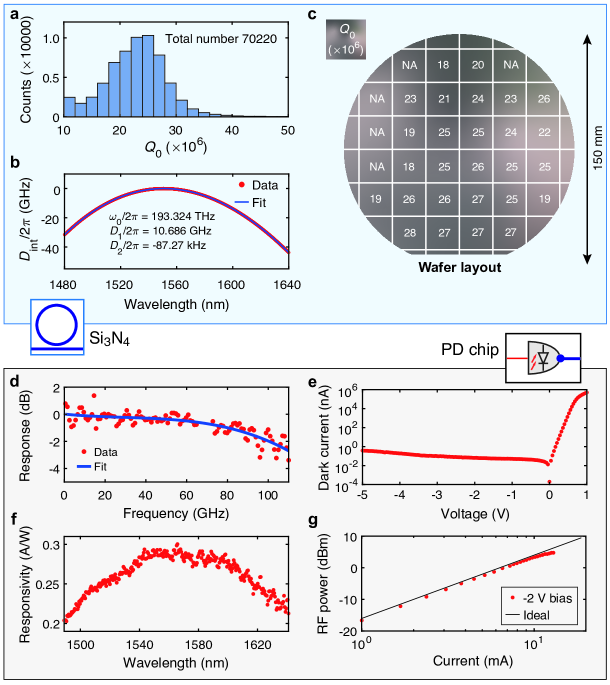
We characterize 70,220 resonances in the fundamental transverse-electric (TE00) mode from 27 chips uniformly distributed over the 6-inch wafer, using a vector spectrum analyzer Luo et al. (2023) covering 1480 to 1640 nm (see Method). The waveguide width of the Si3N4 microresonator is 2.6 m. Each resonance’s intrinsic linewidth and central frequency are measured and fitted. The histogram of intrinsic quality factors of the 70,220 resonances is shown in Fig. 2a. The most probable value is , corresponding to a linear optical loss of dB/m (physical length). Figure 2c shows the measured distribution over the entire wafer, where is found in most places. Such a high value is sufficient for coherent microcomb generation in the Si3N4 microresonator with 37.7 mW power in the bus waveguide.
There are two types of coherent microcombs, i.e. the bright dissipative Kerr soliton (DKS) Herr et al. (2013); Yi et al. (2015); Brasch et al. (2016); Joshi et al. (2016); Liang et al. (2015a), and the dark pulse or platicon Xue et al. (2015); Lobanov et al. (2015); Huang et al. (2015); Parra-Rivas et al. (2016); Nazemosadat et al. (2021). Figure 2b shows the measured microresonator’s integrated dispersion (see definition in Method). Our Si3N4 microresonator features normal group velocity dispersion (GVD, ), permitting platicon generation. In contrast, DKS requires anomalous GVD () that necessitates Si3N4 thickness above 600 nm and specific dispersion engineering Okawachi et al. (2014); Luke et al. (2013).
In addition, we emphasize another two advantages of using platicons instead of DKS for microwave generation. First, compared to DKS, platicons exhibit remarkably higher CW-to-pulse power conversion efficiency Xue et al. (2017); Jang et al. (2021). For 10.7 GHz repetition rate, we achieve power conversion efficiency using platicons (discussed later), while the typical value is for DKS Liu et al. (2020a); Jang et al. (2021). Second, for DKS-based microwave generation, the CW pump must be filtered or blocked before photodetection of the pulse’s repetition rate Liang et al. (2015a); Liu et al. (2020a); Yao et al. (2022). Otherwise, the overwhelmingly strong pump can saturate the PD, yielding deteriorated power and phase noise of the microwave signal. Therefore, a filtering element, e.g. a notch filter, is required in the DKS-based microwave oscillator, which however complicates the overall system and photonic integration. In contrast, platicon-based microwave oscillator does not require such a filter, as in our case. In fact, the presence of the strong CW pump is beneficial. The pump beats against its two neighboring comb lines – with the highest power among all comb lines – and generates strong microwave signal at the repetition rate. In sum, we employ platicons for photonic microwave generation.
Photodetector. The high-speed PD is edge-coupled to the Si3N4 chip’s output waveguide, and is connected by a ground-source-ground (GSG) probe for microwave signal output, as shown in Fig. 1d. The epitaxial structure of the PD chip is grown on a semi-insulating indium phosphide (InP) substrate Li et al. (2023). Figure 1e shows the false-colored scanning electron microscope (SEM) image of the PD’s cross-section and multi-layer structure. The fabrication process of the PD chip starts with P-type contact metals (Ti/Pt/Au/Ti) deposition. Dry etching steps are then performed using inductively coupled plasma etching to form a triple-mesa structure. After the deposition of N-type contact metals (GeAu/Ni/Au), a benzocyclobutene (BCB) layer is implemented beneath the coplanar waveguides (CPWs). This approach eliminates the necessity for air-bridge structures, thus ensuring a consistent and stable connection between p-mesa and CPWs. Details of the fabrication process are found in Supplementary Information.
The frequency response of the InGaAs/InP waveguide device is investigated by an optical heterodyne setup. Upon receiving a heterodyne beatnote between two tunable lasers with wavelengths near 1550 nm, the PD outputs a high-frequency RF signal whose power is measured by a Rohde & Schwarz powermeter (NRP-Z58). Details of the characterization setup are found in Ref. Li et al. (2023). A typical frequency response for m2 PD chip is shown in Fig. 2d. By a polynomial fit of the measured data, 3-dB bandwidth over 110 GHz is shown. The I-V characteristics of the m2 PD chip are measured by a semiconductor device analyzer. Figure 2e shows the measured dark current below 1 nA, which out-performs commercial high-speed PDs. Figure 2f shows the responsivity as high as 0.3 A/W and above 0.2 A/W within 152 nm bandwidth. Figure 2g shows the voltage-dependent saturation property of the PD measured around 10 GHz. The ideal relationship between RF power and DC photo-current is , assuming a 100% modulation depth (), where is the load resistance and is AC photo-current.
Experimental results
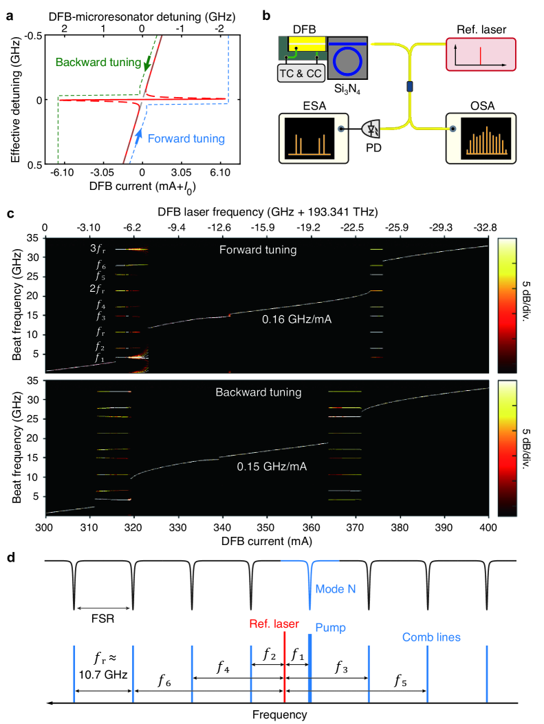
Narrow-linewidth laser and platicon microcomb. First, we characterize the laser dynamics and platicon states with the PD chip removed. The free-running DFB laser’s frequency is increased/decreased by decreasing/increasing the laser driving current. By scanning the DFB current in the forward/backward direction (increasing/decreasing the current) between 300 and 400 mA, the laser frequency is tuned by 32.8 GHz, i.e. with tuning coefficient of GHz/mA. When the laser frequency approaches a microresonator resonance, light is coupled into the Si3N4 microresonator, as shown in Fig. 1a. Due to surface roughness and bulk inhomogeneity of the Si3N4 waveguide, back-scattered light is generated within the microresonator, and is injected back into the laser without an optical isolator. This back-scattered light can trigger laser self-injection locking (SIL) Liang et al. (2015b); Kondratiev et al. (2017, 2023); Voloshin et al. (2021), which locks the laser frequency to the microresonator resonance, as shown in Fig. 3a (see Supplementary Information). The locking range is defined as Kondratiev et al. (2017, 2023)
| (1) |
where is the phase-amplitude factor of the DFB laser, is the coupling efficiency with being the external coupling rate and being the intrinsic loss, is the coupling rate between the counter-propagating modes ( and ) in unit of with , is the DFB laser cavity’s quality factor, is the reflectivity of the output facet of the DFB laser.
Once SIL occurs, the intrinsic laser linewidth is significantly suppressed due to the high quality factor of the Si3N4 microresonator which is much higher than Liang et al. (2015b); Kondratiev et al. (2017, 2023). The suppression ratio of intrinsic laser linewidth can be expresses as
| (2) |
where is the locked laser’s intrinsic linewidth, and is the free-running laser’s intrinsic linewidth. In addition, with sufficient intra-cavity optical power in the Kerr-nonlinear Si3N4 microresonator, nonlinear SIL can lead to DKS Raja et al. (2019); Shen et al. (2020); Voloshin et al. (2021); Pavlov et al. (2018) or platicon formation Jin et al. (2021); Lihachev et al. (2022), depending on the microresonator GVD. In our case with normal GVD, platicons are generated.
The experimental setup to characterize nonlinear SIL dynamics and platicon generation is shown in Fig. 3b. A tunable diode laser (Toptica CTL 1550) is frequency-stabilized to a self-referenced fiber optical frequency comb (Quantum CTek). It serves as a reference laser to beat against the DFB laser emitted from the Si3N4 chip. The beat signal’s frequency is recorded by an electronic spectrum analyser (ESA, Rohde & Schwarz FSW43), and the optical spectrum is recorded by an optical spectrum analyser (OSA, Yokogawa AQ6370D).
As shown in Fig. 3c, while the beat frequency has a global monotonic dependence on the DFB current, it also exhibits multiple flat segments that stay nearly constant when the DFB current varies by less than 10 mA. For example, in the backward tuning, is nearly constant from to mA and from to mA. Such behaviors signal the occurrence of SIL and platicon generation. Degrading SIL performance can be resulted from the presence of the Si3N4 bus waveguide that serves as an extra Fabry-Pérot cavity with weak reflection (see Supplementary information).
The multiple beat frequencies ( to ) in Fig. 3c within the SIL region, e.g. around 320 mA DFB current in the forward tuning, are illustrated in Fig. 3d. Assuming that the pump laser frequency is close to the resonance mode . Then to are the beat frequencies between the reference laser and the platicon’s comb lines including the pump. Meanwhile, ( is an integer) is the beat frequencies among the comb lines, where GHz is the mode spacing (i.e. the platicon’s repetition rate). As the DFB current is tuned to 372 mA in the forward tuning, the laser frequency approaches the resonance mode, leading to another SIL region. Identical behaviors are found in the backward tuning. Considering both directions, the DFB current can be tuned by 12.3 mA in the SIL region, corresponding to a full locking range about 4.0 GHz. Such nonlinear SIL dynamics with platicon generation is similar to the dynamics with DKS generation in Ref. Voloshin et al. (2021).
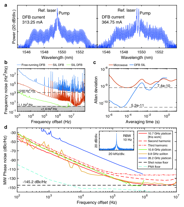
The optical spectra of platicon states at 313.25 and 364.75 mA DFB current in the backward tuning are shown in Fig. 4a. In the SIL region and with 313.25 mA current, the output microcomb power excluding the pump line from the Si3N4 chip is about 1.1 mW. When the DFB laser frequency is off-resonant, the CW output power from the Si3N4 chip is 14 mW. Therefore the CW-to-platicon conversion efficiency is calculated as 8%. Figure 4b shows the optical frequency noise of the SIL laser characterized by a delayed self-heterodyne method Yuan et al. (2022) (see Supplementary Information). The lowest frequency noise is 1.1 Hz2/Hz, corresponding to 6.9 Hz intrinsic linewidth and 31-dB noise suppression on the free-running DFB laser.
Low-noise microwave. The demonstrated narrow linewidth and ultralow noise of the SIL laser are critical for low-noise microwave generation, since the microwave phase noise inherits the laser phase noise with a certain transduction factor Liu et al. (2020a); Tetsumoto et al. (2021). Finally, we edge-couple the PD chip to the Si3N4 chip, enabling photonic microwave generation up to 110 GHz within the PD’s bandwidth. Microwave carriers with frequencies corresponding to the platicon’s repetition rate of GHz and harmonics of are output. Here, we focus on the 10.7 GHz microwave and its second (21.4 GHz in the K-band) and third harmonics (32.1 GHz in the K-band). The RF power exported from the PD chip is // dBm for the 10.7/21.4/32.1 GHz microwave. The 10.7 GHz microwave’s power spectrum is shown in Fig. 4d inset with 6.3 mHz measured linewidth. The microwave’s phase noise is measured with 20-times averaging by a phase noise analyzer (PNA, Rohde & Schwarz FSWP50), as shown in Fig. 4d. The 10.7 GHz microwave’s phase noise reaches // dBc/Hz at 1/10/100 kHz Fourier offset frequency. The phase noise of the second-/third-harmonic microwave is about 6.0/9.5 dB higher, in agreement with the scaling law of ( or ). In comparison, we plot the results in Ref. Jin et al. (2021); Lihachev et al. (2022); Liu et al. (2020a) which use commercial, non-integrated PDs via fiber connection. Figure 4c shows the Allan deviations of the SIL laser frequency and the microwave frequency measured by the PNA. The resemblance in trend indicates that the long term stability of the microwave is dominated by the SIL laser frequency.
Conclusion
In conclusion, we have demonstrated a fully integrated photonic microwave oscillator at 10.7 GHz using a platicon microcomb. Such a hybrid chip device, occupying a footprint of only 76 mm2, consists of a high-power DFB laser, a high- Si3N4 microresonator, and a high-speed PD. Each component represents the state of the art of its own class, yet can be manufactured in large volume with low cost using established CMOS foundries of integrated photonics.
Leveraging laser self-injection locking, the laser frequency noise is suppressed by 31 dB, yielding an intrinsic linewidth of 6.9 Hz and platicon microcomb generation. The PD chip further outputs a 10.7 GHz microwave carrier of 6.3 mHz linewidth, and harmonics of 10.7 GHz benefiting from the PD’s 110 GHz bandwidth. In the future, the long-term stability of the three-in-one – hybrid laser, comb and microwave – can be improved by PDH-locking to an ultra-stable cavity Guo et al. (2022); Cheng et al. (2023). Recent advances Yu et al. (2020); Xiang et al. (2021); Liu et al. (2020b); Snigirev et al. (2023) in heterogeneous integration of III-V, Si3N4 and modulators open a path towards chip devices of further reduced sizes, improved stability and added frequency tunability. Up-shifting the microwave frequency, even into the millimeter-wave band, can be simply realized with Si3N4 microresonators of larger FSR Tetsumoto et al. (2021); Wang et al. (2021) and modified uni-traveling-carrier (MUTC) InP PD chips Li et al. (2023). Such low-noise microwaves from hybrid photonic chips of small size, weight and power consumption can reinvigorate our information technology and applications for microwave photonics, terrestrial broadband, traffic control, tracking, analog-to-digital conversion, wireless networks, space links, and electron paramagnetic resonance spectroscopy.
Methods
Characterization of microresonator dispersion. We use a vector spectrum analyser (VSA) Luo et al. (2023) to measure the central frequency and loaded linewidth of each resonance within 1480 to 1640 nm. The intrinsic loss and external coupling rate can be fitted based on the resonance’s transmission profile Gorodetsky et al. (2000); Li et al. (2013b), extinction ratio Cai et al. (2000) and phase response Luo et al. (2023). The intrinsic () and loaded () quality factors of each resonance can be calculated as and . Due to the presence of microresonator dispersion, the measured resonance grid deviates from an equidistant grid. Thus the resonance frequency can be written as
| (3) | ||||
| (4) |
where is the reference resonance frequency, is the microresonator FSR, describes the GVD, is higher-order dispersion terms. With known , and fitted , the microresonator’s integrated dispersion can be plotted.
Funding Information: J. Liu acknowledges support from the National Natural Science Foundation of China (Grant No.12261131503), Shenzhen-Hong Kong Cooperation Zone for Technology and Innovation (HZQB-KCZYB2020050), and from the Guangdong Provincial Key Laboratory (2019B121203002). B. C. acknowledges support from the National Natural Science Foundation of China (Grant No. 61975121). Z. C. and Y.-H. L. acknowledge support from the China Postdoctoral Science Foundation (Grant No. 2023M731508 and 2022M721482).
Acknowledgments: We thank Zhongkai Wang and Rumin Cheng for assistance in the experiment, Dengke Chen for assistance in data processing, Chengying Bao, Jijun He and Hairun Guo for the fruitful discussion. The DFB lasers were fabricated by Henan Shijia Photons Technology Co., Ltd and Shenzhen PhotonX Technology Co. Ltd. Silicon nitride chips were fabricated by Qaleido Photonics. The PD chips were fabricated with support from the ShanghaiTech University Quantum Device Lab (SQDL).
Author contributions: W. S., Z. C., J. Long, H. Z. performed the experiment with assistance from S. L.. The Si3N4 chips were fabricated by C. S. and L. G., and characterized by B. S. and Y.-H. L.. The PD chips were fabricated by L. L., L. W., Q. C. and B. C.. W. S., Z. C., Y.-H. L., B. C. and J. Liu wrote the manuscript, with the input from others. J. Liu supervised the project.
Disclosures: W. S., Z. C., J. Long and J. Liu are inventors on a patent application related to this work. C. S. and J. Liu are co-founders of Qaleido Photonics, a start-up that is developing heterogeneous silicon nitride integrated photonics technologies. Others declare no conflicts of interest.
Data Availability Statement: The code and data used to produce the plots within this work will be released on the repository Zenodo upon publication of this preprint.
References
- Fortier et al. (2011) T. M. Fortier, M. S. Kirchner, F. Quinlan, J. Taylor, J. C. Bergquist, T. Rosenband, N. Lemke, A. Ludlow, Y. Jiang, C. W. Oates, and S. A. Diddams, Nature Photonics 5, 425 (2011).
- Xie et al. (2016) X. Xie, R. Bouchand, D. Nicolodi, M. Giunta, W. Hänsel, M. Lezius, A. Joshi, S. Datta, C. Alexandre, M. Lours, P.-A. Tremblin, G. Santarelli, R. Holzwarth, and Y. Le Coq, Nature Photonics 11, 44 (2016).
- Li et al. (2014) J. Li, X. Yi, H. Lee, S. A. Diddams, and K. J. Vahala, Science 345, 309 (2014).
- Nakamura et al. (2020) T. Nakamura, J. Davila-Rodriguez, H. Leopardi, J. A. Sherman, T. M. Fortier, X. Xie, J. C. Campbell, W. F. McGrew, X. Zhang, Y. S. Hassan, D. Nicolodi, K. Beloy, A. D. Ludlow, S. A. Diddams, and F. Quinlan, Science 368, 889 (2020).
- Kippenberg et al. (2018) T. J. Kippenberg, A. L. Gaeta, M. Lipson, and M. L. Gorodetsky, Science 361, eaan8083 (2018).
- Pasquazi et al. (2018) A. Pasquazi, M. Peccianti, L. Razzari, D. J. Moss, S. Coen, M. Erkintalo, Y. K. Chembo, T. Hansson, S. Wabnitz, P. Del’Haye, X. Xue, A. M. Weiner, and R. Morandotti, Physics Reports 729, 1 (2018).
- Moss et al. (2013) D. J. Moss, R. Morandotti, A. L. Gaeta, and M. Lipson, Nature Photonics 7, 597 (2013).
- Gaeta et al. (2019) A. L. Gaeta, M. Lipson, and T. J. Kippenberg, Nature Photonics 13, 158 (2019).
- Liu et al. (2021) J. Liu, G. Huang, R. N. Wang, J. He, A. S. Raja, T. Liu, N. J. Engelsen, and T. J. Kippenberg, Nature Communications 12, 2236 (2021).
- Liang et al. (2015a) W. Liang, D. Eliyahu, V. S. Ilchenko, A. A. Savchenkov, A. B. Matsko, D. Seidel, and L. Maleki, Nature Communications 6, 7957 (2015a).
- Liu et al. (2020a) J. Liu, E. Lucas, A. S. Raja, J. He, J. Riemensberger, R. N. Wang, M. Karpov, H. Guo, R. Bouchand, and T. J. Kippenberg, Nature Photonics 14, 486 (2020a).
- Yao et al. (2022) L. Yao, P. Liu, H.-J. Chen, Q. Gong, Q.-F. Yang, and Y.-F. Xiao, Optica 9, 561 (2022).
- Tetsumoto et al. (2021) T. Tetsumoto, T. Nagatsuma, M. E. Fermann, G. Navickaite, M. Geiselmann, and A. Rolland, Nature Photonics 15, 516 (2021).
- Wang et al. (2021) B. Wang, J. S. Morgan, K. Sun, M. Jahanbozorgi, Z. Yang, M. Woodson, S. Estrella, A. Beling, and X. Yi, Light: Science & Applications 10, 4 (2021).
- Li et al. (2013a) J. Li, H. Lee, and K. J. Vahala, Nature Communications 4, 2097 (2013a).
- Li and Vahala (2023) J. Li and K. Vahala, Optica 10, 33 (2023).
- Tang et al. (2018) J. Tang, T. Hao, W. Li, D. Domenech, R. B. nos, P. M. noz, N. Zhu, J. Capmany, and M. Li, Opt. Express 26, 12257 (2018).
- Cundiff and Ye (2003) S. T. Cundiff and J. Ye, Rev. Mod. Phys. 75, 325 (2003).
- Fortier and Baumann (2019) T. Fortier and E. Baumann, Communications Physics 2, 153 (2019).
- Diddams et al. (2020) S. A. Diddams, K. Vahala, and T. Udem, Science 369, eaay3676 (2020).
- Herr et al. (2013) T. Herr, V. Brasch, J. D. Jost, C. Y. Wang, N. M. Kondratiev, M. L. Gorodetsky, and T. J. Kippenberg, Nature Photonics 8, 145 (2013).
- Yi et al. (2015) X. Yi, Q.-F. Yang, K. Y. Yang, M.-G. Suh, and K. Vahala, Optica 2, 1078 (2015).
- Brasch et al. (2016) V. Brasch, M. Geiselmann, T. Herr, G. Lihachev, M. H. P. Pfeiffer, M. L. Gorodetsky, and T. J. Kippenberg, Science 351, 357 (2016).
- Joshi et al. (2016) C. Joshi, J. K. Jang, K. Luke, X. Ji, S. A. Miller, A. Klenner, Y. Okawachi, M. Lipson, and A. L. Gaeta, Opt. Lett. 41, 2565 (2016).
- Xue et al. (2015) X. Xue, Y. Xuan, Y. Liu, P.-H. Wang, S. Chen, J. Wang, D. E. Leaird, M. Qi, and A. M. Weiner, Nature Photonics 9, 594 (2015).
- Kovach et al. (2020) A. Kovach, D. Chen, J. He, H. Choi, A. H. Dogan, M. Ghasemkhani, H. Taheri, and A. M. Armani, Adv. Opt. Photon. 12, 135 (2020).
- Chang et al. (2022) L. Chang, S. Liu, and J. E. Bowers, Nature Photonics 16, 95 (2022).
- Kudelin et al. (2023) I. Kudelin, W. Groman, Q.-X. Ji, J. Guo, M. L. Kelleher, D. Lee, T. Nakamura, C. A. McLemore, P. Shirmohammadi, S. Hanifi, H. Cheng, N. Jin, S. Halliday, Z. Dai, L. Wu, W. Jin, Y. Liu, W. Zhang, C. Xiang, V. Iltchenko, O. Miller, A. Matsko, S. Bowers, P. T. Rakich, J. C. Campbell, J. E. Bowers, K. Vahala, F. Quinlan, and S. A. Diddams, arXiv 2307.08937 (2023).
- Sun et al. (2023) S. Sun, B. Wang, K. Liu, M. Harrington, F. Tabatabaei, R. Liu, J. Wang, S. Hanifi, J. S. Morgan, M. Jahanbozorgi, Z. Yang, S. Bowers, P. Morton, K. Nelson, A. Beling, D. Blumenthal, and X. Yi, arXiv 2305.13575 (2023).
- Jin et al. (2024) X. Jin, Z. Xie, X. Zhang, H. Hou, F. Zhang, X. Zhang, Q. Gong, L. Chang, and Q.-F. Yang, arXiv 2401.12760 (2024).
- He et al. (2024) Y. He, L. Cheng, H. Wang, Y. Zhang, R. Meade, K. Vahala, M. Zhang, and J. Li, arXiv 2402.16229 (2024).
- Stern et al. (2018) B. Stern, X. Ji, Y. Okawachi, A. L. Gaeta, and M. Lipson, Nature 562, 401 (2018).
- Raja et al. (2019) A. S. Raja, A. S. Voloshin, H. Guo, S. E. Agafonova, J. Liu, A. S. Gorodnitskiy, M. Karpov, N. G. Pavlov, E. Lucas, R. R. Galiev, A. E. Shitikov, J. D. Jost, M. L. Gorodetsky, and T. J. Kippenberg, Nature Communications 10, 680 (2019).
- Shen et al. (2020) B. Shen, L. Chang, J. Liu, H. Wang, Q.-F. Yang, C. Xiang, R. N. Wang, J. He, T. Liu, W. Xie, J. Guo, D. Kinghorn, L. Wu, Q.-X. Ji, T. J. Kippenberg, K. Vahala, and J. E. Bowers, Nature 582, 365 (2020).
- Lihachev et al. (2022) G. Lihachev, W. Weng, J. Liu, L. Chang, J. Guo, J. He, R. N. Wang, M. H. Anderson, Y. Liu, J. E. Bowers, and T. J. Kippenberg, Nature Communications 13, 1771 (2022).
- Ye et al. (2023) Z. Ye, H. Jia, Z. Huang, C. Shen, J. Long, B. Shi, Y.-H. Luo, L. Gao, W. Sun, H. Guo, J. He, and J. Liu, Photon. Res. 11, 558 (2023).
- Luke et al. (2013) K. Luke, A. Dutt, C. B. Poitras, and M. Lipson, Opt. Express 21, 22829 (2013).
- Muñoz et al. (2019) P. Muñoz, P. W. L. van Dijk, D. Geuzebroek, M. Geiselmann, C. Domínguez, A. Stassen, J. D. Doménech, M. Zervas, A. Leinse, C. G. H. Roeloffzen, B. Gargallo, R. Baños, J. Fernández, G. M. Cabanes, L. A. Bru, and D. Pastor, IEEE Journal of Selected Topics in Quantum Electronics 25, 1 (2019).
- Xiang et al. (2022) C. Xiang, W. Jin, and J. E. Bowers, Photon. Res. 10, A82 (2022).
- Luo et al. (2023) Y.-H. Luo, B. Shi, W. Sun, R. Chen, S. Huang, Z. Wang, J. Long, C. Shen, Z. Ye, H. Guo, and J. Liu, arXiv 2304.04295 (2023).
- Lobanov et al. (2015) V. Lobanov, G. Lihachev, T. J. Kippenberg, and M. Gorodetsky, Opt. Express 23, 7713 (2015).
- Huang et al. (2015) S.-W. Huang, H. Zhou, J. Yang, J. F. McMillan, A. Matsko, M. Yu, D.-L. Kwong, L. Maleki, and C. W. Wong, Phys. Rev. Lett. 114, 053901 (2015).
- Parra-Rivas et al. (2016) P. Parra-Rivas, D. Gomila, E. Knobloch, S. Coen, and L. Gelens, Optics Letters 41, 2402 (2016).
- Nazemosadat et al. (2021) E. Nazemosadat, A. Fülöp, O. B. Helgason, P.-H. Wang, Y. Xuan, D. E. Leaird, M. Qi, E. Silvestre, A. M. Weiner, and V. Torres-Company, Phys. Rev. A 103, 013513 (2021).
- Okawachi et al. (2014) Y. Okawachi, M. R. E. Lamont, K. Luke, D. O. Carvalho, M. Yu, M. Lipson, and A. L. Gaeta, Opt. Lett. 39, 3535 (2014).
- Xue et al. (2017) X. Xue, P.-H. Wang, Y. Xuan, M. Qi, and A. M. Weiner, Laser & Photonics Reviews 11, 1600276 (2017).
- Jang et al. (2021) J. K. Jang, Y. Okawachi, Y. Zhao, X. Ji, C. Joshi, M. Lipson, and A. L. Gaeta, Opt. Lett. 46, 3657 (2021).
- Li et al. (2023) L. Li, L. Wang, and B. Chen, in 2023 Opto-Electronics and Communications Conference (OECC) (2023) pp. 1–3.
- Jin et al. (2021) W. Jin, Q.-F. Yang, L. Chang, B. Shen, H. Wang, M. A. Leal, L. Wu, M. Gao, A. Feshali, M. Paniccia, K. J. Vahala, and J. E. Bowers, Nature Photonics 15, 346 (2021).
- Liang et al. (2015b) W. Liang, V. S. Ilchenko, D. Eliyahu, A. A. Savchenkov, A. B. Matsko, D. Seidel, and L. Maleki, Nature Communications 6, 7371 (2015b).
- Kondratiev et al. (2017) N. M. Kondratiev, V. E. Lobanov, A. V. Cherenkov, A. S. Voloshin, N. G. Pavlov, S. Koptyaev, and M. L. Gorodetsky, Optics Express 25, 28167 (2017).
- Kondratiev et al. (2023) N. M. Kondratiev, V. E. Lobanov, A. E. Shitikov, R. R. Galiev, D. A. Chermoshentsev, N. Y. Dmitriev, A. N. Danilin, E. A. Lonshakov, K. N. Min’kov, D. M. Sokol, S. J. Cordette, Y.-H. Luo, W. Liang, J. Liu, and I. A. Bilenko, Frontiers of Physics 18, 21305 (2023).
- Voloshin et al. (2021) A. S. Voloshin, N. M. Kondratiev, G. V. Lihachev, J. Liu, V. E. Lobanov, N. Y. Dmitriev, W. Weng, T. J. Kippenberg, and I. A. Bilenko, Nature Communications 12, 235 (2021).
- Pavlov et al. (2018) N. G. Pavlov, S. Koptyaev, G. V. Lihachev, A. S. Voloshin, A. S. Gorodnitskiy, M. V. Ryabko, S. V. Polonsky, and M. L. Gorodetsky, Nature Photonics 12, 694 (2018).
- Yuan et al. (2022) Z. Yuan, H. Wang, P. Liu, B. Li, B. Shen, M. Gao, L. Chang, W. Jin, A. Feshali, M. Paniccia, J. Bowers, and K. Vahala, Opt. Express 30, 25147 (2022).
- Guo et al. (2022) J. Guo, C. A. McLemore, C. Xiang, D. Lee, L. Wu, W. Jin, M. Kelleher, N. Jin, D. Mason, L. Chang, A. Feshali, M. Paniccia, P. T. Rakich, K. J. Vahala, S. A. Diddams, F. Quinlan, and J. E. Bowers, Science Advances 8, eabp9006 (2022).
- Cheng et al. (2023) H. Cheng, N. Jin, Z. Dai, C. Xiang, J. Guo, Y. Zhou, S. A. Diddams, F. Quinlan, J. Bowers, O. Miller, and P. Rakich, APL Photonics 8, 116105 (2023).
- Yu et al. (2020) Q. Yu, J. Gao, N. Ye, B. Chen, K. Sun, L. Xie, K. Srinivasan, M. Zervas, G. Navickaite, M. Geiselmann, and A. Beling, Opt. Express 28, 14824 (2020).
- Xiang et al. (2021) C. Xiang, J. Liu, J. Guo, L. Chang, R. N. Wang, W. Weng, J. Peters, W. Xie, Z. Zhang, J. Riemensberger, J. Selvidge, T. J. Kippenberg, and J. E. Bowers, Science 373, 99 (2021).
- Liu et al. (2020b) J. Liu, H. Tian, E. Lucas, A. S. Raja, G. Lihachev, R. N. Wang, J. He, T. Liu, M. H. Anderson, W. Weng, S. A. Bhave, and T. J. Kippenberg, Nature 583, 385 (2020b).
- Snigirev et al. (2023) V. Snigirev, A. Riedhauser, G. Lihachev, M. Churaev, J. Riemensberger, R. N. Wang, A. Siddharth, G. Huang, C. Möhl, Y. Popoff, U. Drechsler, D. Caimi, S. Hönl, J. Liu, P. Seidler, and T. J. Kippenberg, Nature 615, 411 (2023).
- Gorodetsky et al. (2000) M. L. Gorodetsky, A. D. Pryamikov, and V. S. Ilchenko, J. Opt. Soc. Am. B 17, 1051 (2000).
- Li et al. (2013b) Q. Li, A. A. Eftekhar, Z. Xia, and A. Adibi, Phys. Rev. A 88, 033816 (2013b).
- Cai et al. (2000) M. Cai, O. Painter, and K. J. Vahala, Phys. Rev. Lett. 85, 74 (2000).