Direct visualization of defect-controlled diffusion in van der Waals gaps
Abstract
Diffusion processes govern fundamental phenomena such as phase transformations, doping, and intercalation in van der Waals (vdW) bonded materials. Here, we quantify the diffusion dynamics of W atoms by visualizing the motion of individual atoms at three different vdW interfaces, BN/vacuum, BN/BN, and BN/WSe2, using scanning transmission electron microscopy movies. Supported by density functional theory calculations, we infer that in all cases diffusion is governed by intermittent trapping at electron beam-generated defect sites. This leads to diffusion properties that depend strongly on the number of defects. These results suggest that diffusion and intercalation processes in vdW materials are highly tunable and sensitive to crystal quality. Furthermore, the demonstration of atomic resolution imaging of materials inside vdW heterostructures offers possibilities for direct visualization of diffusion and atomic interactions, as well as for experiments exploring atomic structures, their in-situ modification, and electrical property measurement.
I Introduction
Diffusion of atomic species in and on two-dimensional (2D) materials governs numerous phenomena such as phase transformations [1], crystal growth [2], and doping [3, 4]. In particular, the diffusion of foreign atoms into van der Waals (vdW) bonded materials to form intercalated structures has great potential for tuning physical properties (electronic, optoelectronic, magnetic), and for uses in energy storage and catalysis [5, 6]. Furthermore, vdW heterostructures consisting of 2D materials encapsulated by hexagonal boron nitride (BN) are the de facto standard for creating devices with high-quality electrical properties [7]. Diffusion processes in these vdW heterostructures are interesting because such structures show promise for novel electronic, optoelectronic [8, 9], and magnetic devices [10, 11] and offer possibilities for exploring phenomena such as strongly correlated electron physics [12]. A microscopic understanding of diffusion pathways and dynamics and the role of defects is critical for tailoring the properties of these structures. TEM offers possibilities for real-time, atomic resolution imaging of diffusion processes, and has been used to image the diffusion of adsorbed or substitutional atoms on the surface of different 2D materials [13, 14, 15].
Here, we directly visualize the atomic scale dynamics of W diffusion inside a vdW heterostructure, at the interfaces between BN/BN, BN/WSe2, and BN/vacuum. We show that the diffusion properties are governed by defects at the interfaces, which create trapping sites for W atoms. This leads to diffusion properties that are more affected by defect densities than the details of the interface structure such as the size of the vdW gap.
The ability to image the dynamics of atoms embedded inside vdW heterostructures with high spatial and temporal resolution offers opportunities for quantifying other diffusion processes and atomic interactions, as well as the prospect of combining electrical and structural measurements through careful experimental design.
II Atomic motion in the van der Waals gap
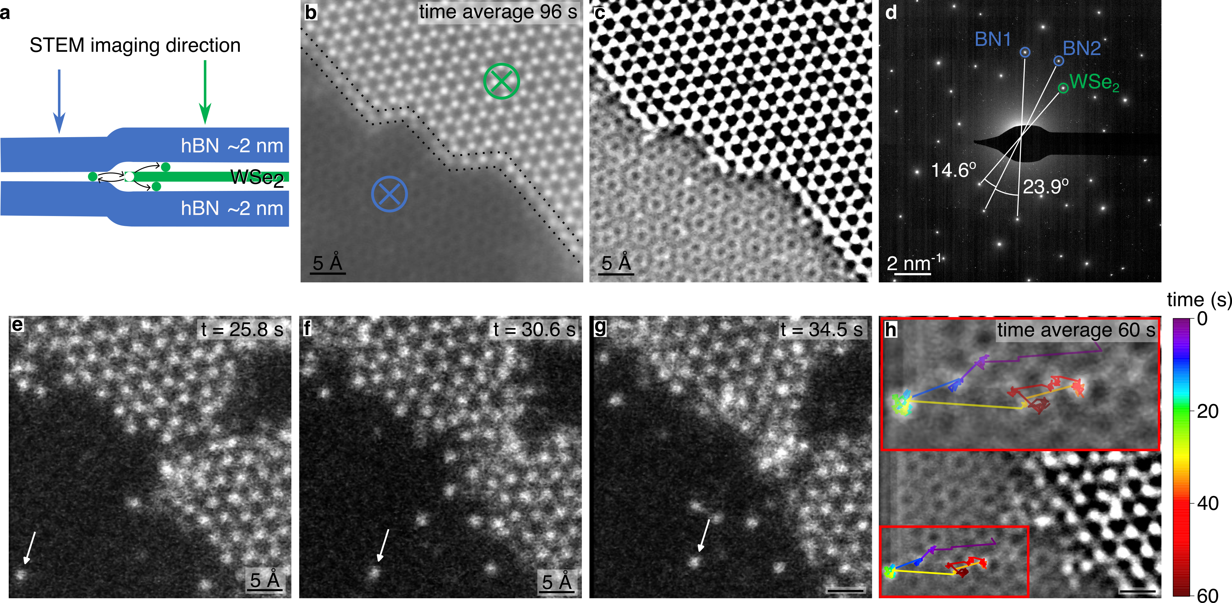
To study the atomic motion of W atoms at vdW-bonded interfaces, we fabricated BN/WSe2/BN heterolayer stacks with monolayer WSe2 and 2 nm thick BN. Details of sample fabrication are described in Methods. By choosing WSe2 crystals that were laterally smaller than the BN crystals, we embedded an edge of WSe2 within the heterostructure. This served as the source of W (and Se) atoms, as discussed below. A schematic of this BN/WSe2/BN heterostructure is shown in Fig. 1(a). Optical microscopy images of the samples are given in Figs. S1 and S2. Such samples allow us to make quantitative comparisons between the diffusion of W atoms at the BN/WSe2 and BN/BN interfaces. We measure diffusion at the BN/vacuum interface by creating simpler BN/WSe2 heterostructures, still with laterally smaller WSe2 crystals. The sensitivity of HAADF-STEM for heavier atoms allows us to image the monolayer WSe2 and individual diffusing W atoms at atomic resolution through the BN layers (Fig. 1(b, c), Supplementary Video 1). Although individual Se atoms were also mobile and visible within the sample, we tracked the motion of W atoms because they appear brighter in HAADF-STEM imaging, as contrast scales with atomic mass as Z1.7 [16]. The layers were not rotationally aligned during the stacking process, and the rotational misalignment of the three layers can be measured from diffraction, as in Fig. 1(d). We use fixed conditions (electron beam energy and current, dwell time, magnification, and number of pixels per image) for all data used to quantify diffusion dynamics (see Methods for imaging conditions and data analysis). All data shown in the main text is obtained with an electron beam energy of 200 keV and we provide additional data obtained at 60 keV in the Supplementary Information.
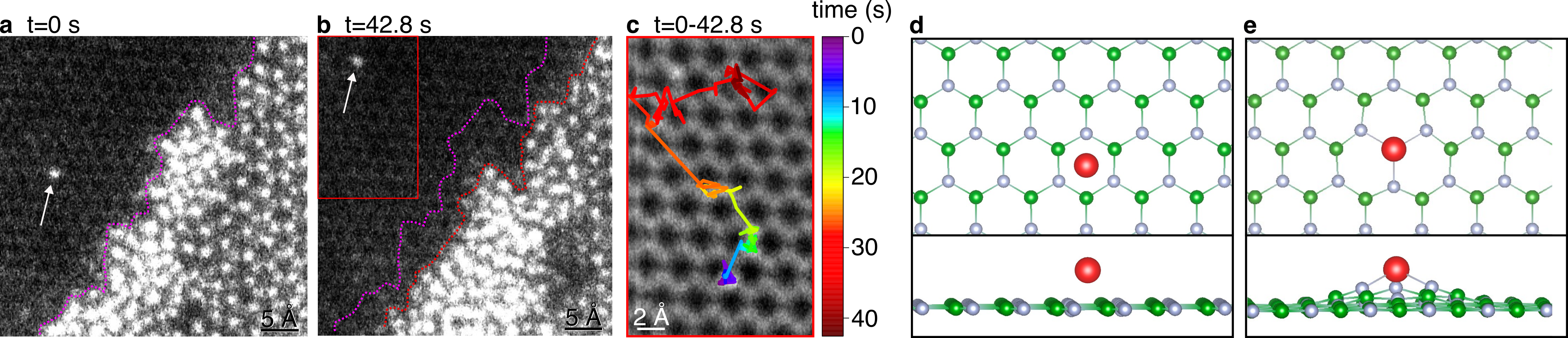
During imaging of these structures we then locate mobile W atoms that originate from the WSe2 lattice. They can either diffuse between the two BN sheets or at the interface between the WSe2 and BN. Figure 1(e-g) shows images of a tracked W atom diffusing at the BN/BN interface, see also Supplementary Video 2. Figure 1(h) is an averaged image from the video with the trajectory of the W atom shown on top. From such trajectories we can study the atomic scale dynamics and statistics or the W atom motion at the different interfaces. In the following sections we describe and analyze the formation of diffusing W atoms and W diffusion process at the atomic scale at the WSe2/BN, BN/BN, and BN/vacuum interfaces.
II.1 Diffusion at the BN/WSe2 interface
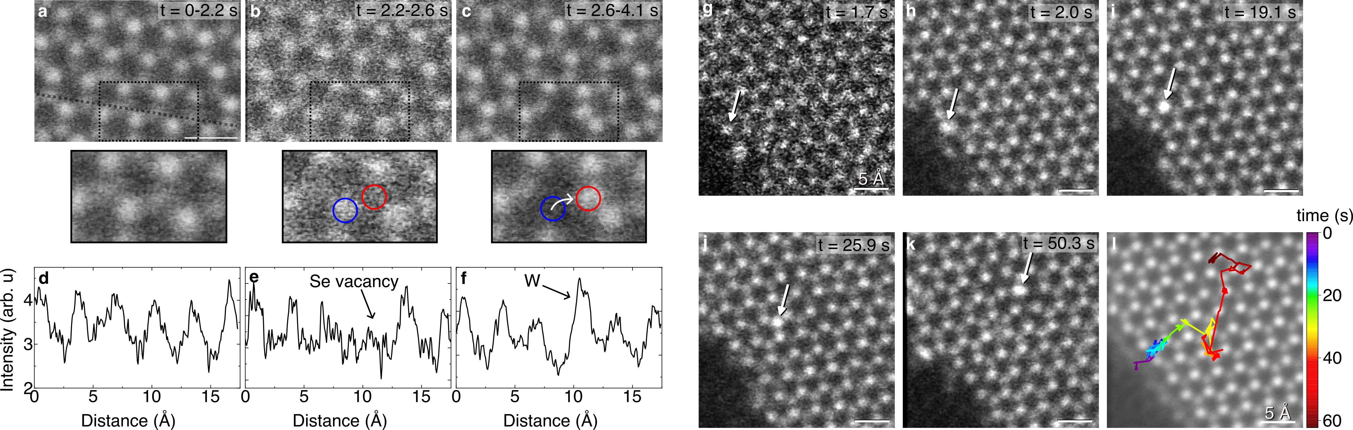
We first discuss the origin of the moving W atoms at the BN/WSe2 interface. Upon initially imaging a pristine BN/WSe2/BN region, we observe that W ejection from the bulk WSe2 is preceded consistently by the formation of neighboring single or double selenium vacancies (Fig. 2(a-c), Supplementary Video 3). Another example is given in Fig. S3. This takes place on a timescale of approximately 1 min. The knock-on threshold for W atoms in a pristine WSe2 lattice is above 500 keV while the threshold for Se atoms is 190 keV [17]. The observation of Se vacancy formation as the first step of the process is therefore consistent with a beam-driven effect.
We have also observed W atoms at the edge of the WSe2 lattice diffuse into the BN/WSe2 interface (Supplementary Video 4). Figure 2(g-k) shows images with a moving W atom indicated by a white arrow. Figure 2(l) shows the trajectory of the atom.
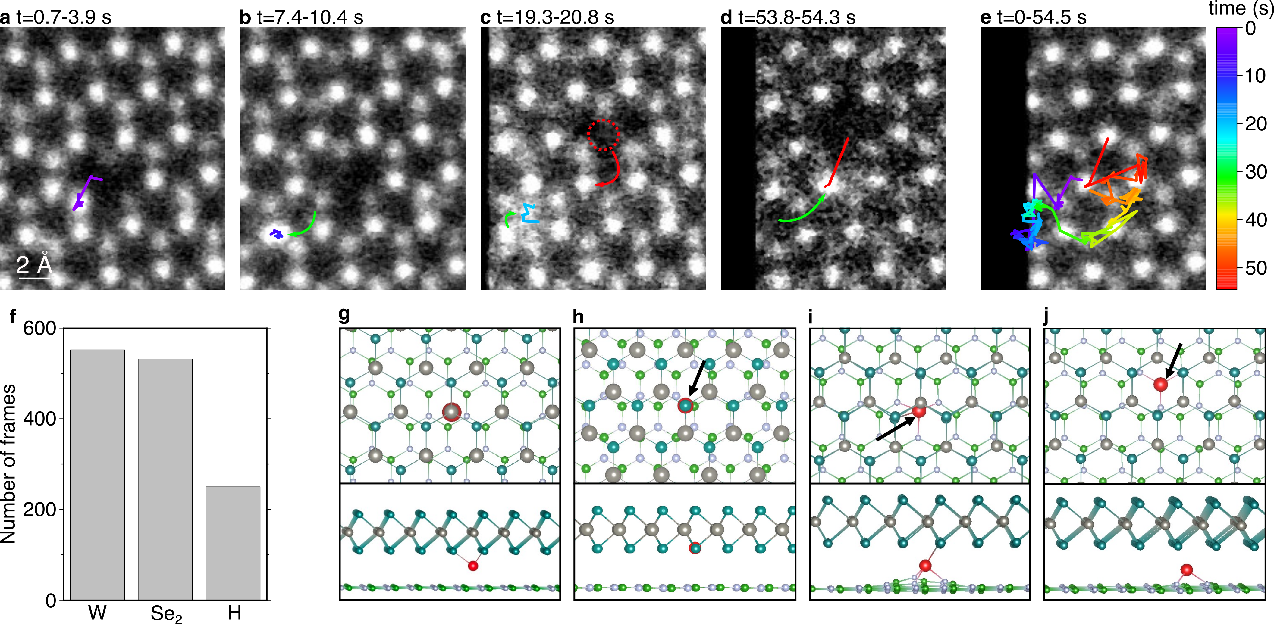
After their release from the WSe2 lattice we track the diffusion behavior of single W atoms at the BN/WSe2 interface. Figure 3(a-d) and Supplementary Video 5 follows a W atom as it is ejected from the WSe2 lattice and sits at different times in a Se2 site (Fig. 3(a)), a W site (Fig. 3(b)), and a hexagonal or “hollow” (H) site (Fig. 3(c)). It finally becomes reincorporated into the WSe2 lattice (Fig. 3(d)), albeit at a different location from its origin because the W vacancy diffused a distance of one unit cell, as shown in Fig. 3(c). Since the W atom can reincorporate into the WSe2 lattice, this suggests that the W atoms diffuse directly at the BN/WSe2 interface. Figure 3(e) displays the total trajectory. See Fig. S4 and S5 for trajectories of additional W atoms measured at the BN/WSe2 interface. The data shown in Fig. 3, Fig. S4, and S5 are consistent in that the W atoms reside on W and Se2 sites at about the same rate, 41% and 40% of frames, respectively, while they reside on a H site on 19% of frames (Fig. 3(f), see Methods for details).
We next compare the statistics in Fig. 3(h) with expectations from DFT calculations (Methods) to better understand the potential landscape of interstitial W atoms. We find that the most stable site for an interstitial W atom in a pristine WSe2/BN interface is at another W site (Fig. 3(g)). We then introduce vacancies into the system. A Se vacancy (Fig. 3(h) or any B vacancy (Fig. 3(i, j)), unsurprisingly, become significantly more stable sites for the W atom, as the W atom can form bonds to the three neighboring W or N atoms in the case of the Se or B vacancy, respectively.
If vacancies in the BN were to completely determine W pinning sites, then we would expect W atoms to reside equally on W, Se2, and H sites since vacancies in the BN layers would be distributed above these sites equally. Since we find that W atoms reside mainly on W and Se sites, this indicates that the potential landscape of WSe2 also plays a role in determining pinning sites. The equal prevalence of W and Se sites might further be due to the presence of Se vacancies. Hence, analysis of the preferential resting sites for these interstitial atoms reveal that their motion is influenced by the presence of Se vacancies in the WSe2 as well as B or N vacancies in the adjacent BN layers. In the following we will show that W diffusion at the BN/BN interface exhibits similar characteristics.
II.2 Diffusion at the BN/BN interface
Upon imaging a pristine BN/BN region near a WSe2 edge, we find several mobile W atoms. We assume that these atoms are detached from the WSe2 edge through interactions with the 200 kV electron beam because undercoordinated edge atoms are easier to eject. We find that the edge does not retract noticeably over extended periods of time (Fig. 1(b)), but edge atoms detach and reattach analogous to a sublimation and deposition process on a surface. Only the outer row of atoms on the WSe2 edge (highlighted in Fig. 1(b)) appears blurry in the time averaged-image (over 96 s) due to their motion.
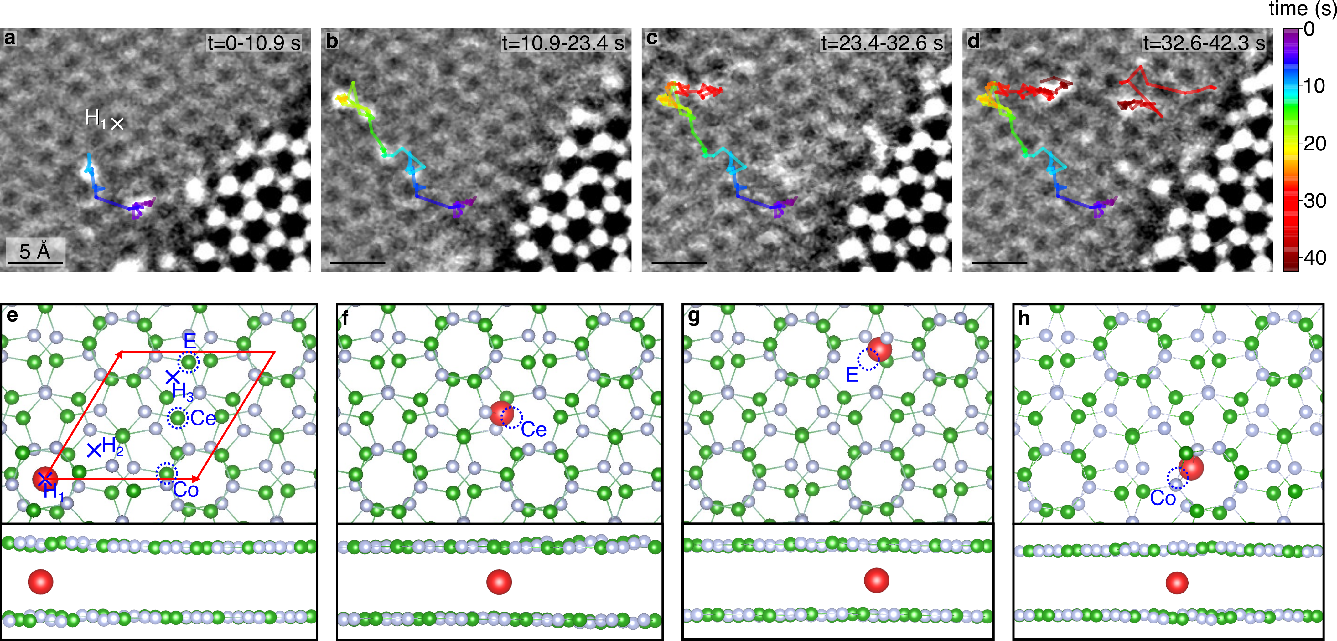
To quantify the atomic scale details of W diffusion in the BN/BN interface, Fig. 1(e-h) and Fig. 4(a-d) show trajectories of W atoms at high magnification. See Fig. S6 and S7 for trajectories of additional W atoms at the BN/BN interface. The atoms make several smaller displacements, 1 Å, seemingly around pinning sites, and fewer, larger displacements between such sites. We observe that the W atoms reside mainly on the moiré lattice of the BN/BN interface, i.e. on BN lattice sites. We compare this observation to DFT calculations for stable resting sites at the BN/BN interface. Figure 4(e) shows the model of the BN/BN interface that we used for these calculations (Methods). The moiré unit cell features some distinctive sites that are indicated with blue circles and crosses in Fig. 4(e). The largest hollow space, denoted H1, is present at the corners of the unit cell, while smaller hollow spaces are denoted by H2 and H3. Figure 4(e) shows that for a pristine BN/BN interface, the most stable site for the W atom is at H1. This corresponds to the center of the “donut” shapes in Fig. 4(d) (marked with a white cross). Configurations with W atoms at H2 and H3 display about 200 meV higher energy than a configuration with a W atom at H1 (Fig. S8). However, introducing a B vacancy at three distinct lattice sites on the moiré unit cell, namely the center (Ce), edge (E), and corner (Co) sites (Fig. 4(f-h)) makes these sites significantly more stable positions for the W atoms. For example, in the case of an E site, the DFT calculations show that the total energy of the system increases by 7 eV when moving a W atom from E to H1, see Fig. S9, because 3 W-N bonds must be broken. This means that B vacancy sites are significantly more stable sites for W interstitials as compared to the ‘best’ H1 site in the pristine interface.
Overall, DFT simulations predict that the H1 site should be the most stable resting site for W atoms in a pristine interface. However, we find experimentally that W atoms reside on the BN/BN moiré lattice in agreement with our DFT predictions that vacancies in the Ce, E, or Co sites are significantly more stable sites. These results therefore suggest that defects formed by the electron beam govern resting sites and diffusion properties at the BN/BN interface. This behavior is consistent with that seen for the BN/WSe2 interface.
II.3 Diffusion at the BN/vacuum interface
We finally image W atoms on the free surface of BN for comparison with the situations described above where the W atoms are encapsulated. Figure 5(a, b) display the first and last image, respectively, from a video where we track an atom. These images reveal that the WSe2 edge recedes over time, with dislodged W/Se atoms aggregating in a structure on the edge that appears three dimensional, based on the proximity of the W atoms in projection. This behavior differs from the BN encapsulated WSe2 edge, where spatial confinement evidently prevents atoms on the WSe2 edge from forming a 3D structure, so they instead detach and reattach in a 2D fashion (Fig. 1(a)). Figure 5(c) shows an average of the entire video with the atom trajectory shown on top. We find that the atom makes several smaller displacements less than approximately an atomic spacing around a pinning site and fewer larger displacements over several atomic spacings in between such sites. Furthermore, we see that the pinning sites coincide with positions on the BN lattice.
Figure 5(d) shows results from DFT calculations that predict the most stable site for W atoms on a pristine BN surface is in the hollow site, as minimal orbital overlap gives the maximum spacing for the adatom. Adding a B vacancy (Fig. 5(e)) makes the vacancy by far the most stable site for W adatoms. Our experimental observation that W atoms occupy lattice sites on the BN is therefore consistent with the importance of defects in the BN layer in determining pinning sites.
II.4 Statistics of the atomic motion at each interface
Having shown qualitatively that W atoms appear to move through displacements between defect sites, we focus now on a quantitative analysis of the time-dependence of this behavior. This quantitative analysis simplifies considerably if the diffusion coefficient does not depend on direction. Therefore, we first investigated the diffusion isotropy, see Fig. S10–S13. We found that the diffusion is isotropic except for the shortest displacements, less than one atomic spacing. These display some degree of anisotropy aligned with the axes of the image, implying that the result is due to measurement artifacts (see caption Fig. S10). We further note that we do not find any evidence that the motion is affected by the electron beam scanning direction.
Since defects are continuously produced by the electron beam during the experiment, we expect a gradual increase in the frequency with which diffusing atoms are trapped on defects. This lowers the diffusion coefficient over time. To test this hypothesis, we next investigate the time-dependent diffusion coefficient.
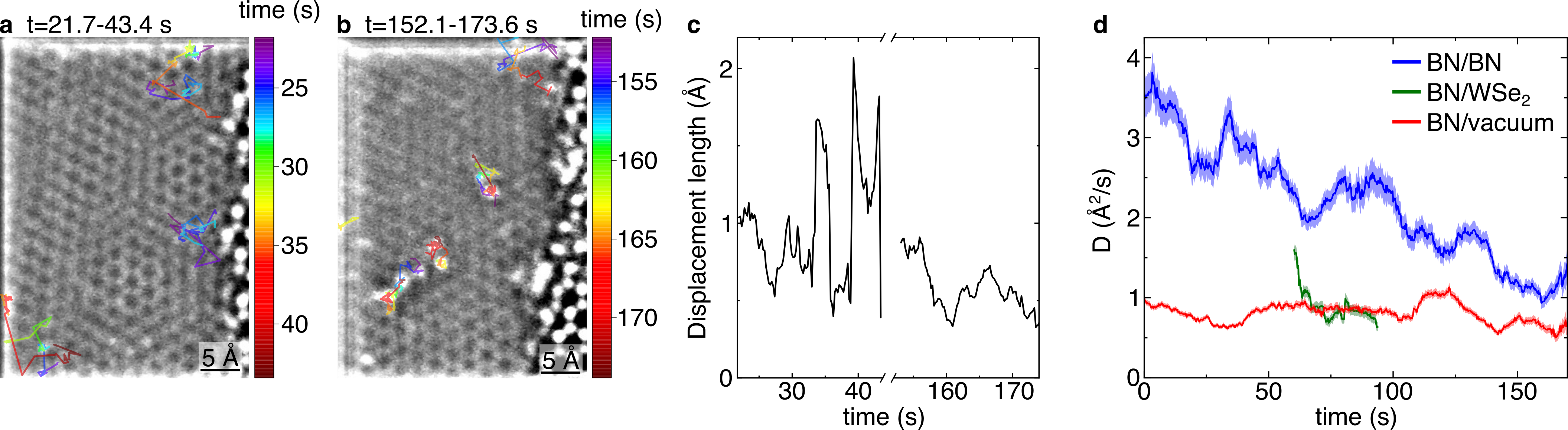
We performed experiments where we acquired data for 170 s from approximately the same area of a sample, by minimizing sample drift, and measured the diffusivity of the atoms in these videos. For this data, we define t=0 as the time where a pristine area on the sample is first imaged. For the BN/BN interface we observe a marked decrease in W atom diffusivity. This is visible, for example, in data such as Supplementary Video 8, which was recorded from t=0. Such a trend is not apparent for the BN/WSe2 and BN/vacuum interfaces as we will show and discuss below. Figure 6(a) shows W atom trajectories from early times (100 frames, corresponding to 21.7 s) of such an experiment while Fig. 6(b) shows W atom trajectories from the last 21.7 s from the same experiment. We find that their average displacement length decreases over time (Fig. 6(c)).
We then average across all trajectories recorded to find the overall behavior of W atoms at each interface. The diffusion coefficient, , is optimally estimated using a co-variance based estimator [18] (Methods). We used this method on all displacements observed within a rolling time-window of 15 s to elucidate the time-dependence of the diffusion coefficient.
Figure 6(d) shows the W diffusion coefficient plotted against time for each interface. For the BN/BN interface, decreases over time, starting at a value of 3.5 Å2/s at t=0 s and ending at a value of 1.5 Å2/s at t=150 s. We expect the initial value of 3.5 Å2/s is a lower bound of because we find that the W atoms initially undergo large displacements which are challenging to track. When several atoms are present near each other this would result in an underestimation of their displacements with the nearest-neighbor tracking algorithm (see Methods) we used.
Imaging beyond approx. 150 s results in the loss of BN/BN moiré image intensity, see Fig. S14-S16. This indicates damage in the BN structure, and hence is consistent with the hypothesis that the decreasing diffusion coefficient is due to the continuous introduction of defects until the interface is destroyed and becomes amorphous. Such an interpretation is supported by literature. It is known that electron beam generated defects are not created uniformly through the thickness of a 2D material, but form more readily at the bottom surface [19]. TEM experiments in literature with BN have also shown that BN tends to be removed in a layer-by-layer fashion from the bottom surface with 6 electrons/Å2 needed for the removal of a layer [20]. We use a beam current of 50 pA to scan a 44 nm area, giving a dose rate of 2 electrons/Å2/s. Thus, we need 30 s to remove a BN monolayer, fitting well with our observation of 150 s needed to etch through 2 nm of BN, corresponding to 6 monolayers of BN.
In addition, experiments at 60 kV show that degradation of the BN/BN interface and formation of W vacancies in bulk WSe2 occurs at significantly longer time scales. At 60 kV, imaging beyond 400-600 s is needed before any noticeable BN/BN moiré intensity loss (Fig. S17 and S18, Supplementary Video 9). Imaging the BN/WSe2 interface, a pristine region was imaged for almost 400 s before the formation of a W vacancy (Fig. S19, Supplementary Video 10). Thus, defect formation is highly dependent on electron beam energy, and use of lower electron beam energies may be a viable strategy for observing a sample without significant defect formation or modification.
At the BN/vacuum interface, the diffusion coefficient for W atoms fluctuates around a value of 0.8 Å2/s. In literature, the diffusivity of intercalated atoms in vdW materials has been shown to increase with interlayer distance [21, 22]. Hence, intuitively one would expect that atoms diffusing on the free surface of BN would display faster diffusion compared to atoms diffusing in a vdW-bonded interface. We believe that two factors may account for the the lower diffusivity at the BN/vacuum interface compared to the BN/BN interface. First, polymeric contamination is ubiquitous on the surface of 2D materials samples that have been transferred to TEM grids using polymer handles [23]. Such carbon-containing contamination is challenging to image through a multilayer due to its low atomic mass and is known to pin atoms diffusing on the surface of 2D materials [24]. Second, the data from the BN/vacuum interface comes from a sample where W atoms diffused on the bottom side of the BN with respect to electron beam direction. The bottom surface of a 2D material is more prone to electron beam induced defects, since atoms can be removed more easily by direct knock-on damage [17]. That the diffusion coefficient of W atoms at the BN/vacuum is significantly smaller than that of W atoms at the BN/BN interface suggests that the diffusion properties are less affected by interlayer distances, and more strongly depend on the defect concentration and the presence of contamination on the sample.
Finally, for the BN/WSe2 interface, we find that W atoms are released from the WSe2 lattice typically after at least 60 s of imaging. The start of each recorded trajectory is therefore set to t=60 s. appears to be decreasing initially and then fluctuates around a value of 0.8 Å2/s, the same as the diffusion coefficient of W atoms at the BN/vacuum interface. This may be the result of the amount of imaging typically needed to release W atoms from bulk WSe2, where by the time W is released the interface is already markedly damaged.
Combining information for all three interfaces, we conclude that the comparative values and their variation with time are consistent with atomic motion dominated by impurities and defects that are created by the electron beam at the interface.
III Conclusions
We have quantified diffusion of W atoms at the BN/vacuum, BN/BN, and BN/WSe2 interfaces with atomic resolution imaging of single atoms through several atomic layers of BN, measuring not only diffusion parameters but also atomistic diffusion pathways. Our results show that the diffusion properties of W atoms in vdW bonded interfaces are tunable and highly affected by defects at the interface. We determine this by directly visualizing trapping sites during the diffusion and comparing with expectations from DFT calculation. We further quantify diffusion properties and find a strong impact of defect concentration on the diffusion coefficient of W atoms at the BN/BN interface resulting in a time-dependent diffusion coefficient as a result of defects added during STEM imaging at 200 kV acceleration voltage. In addition, we have performed experiments with a 60 kV acceleration voltage showing the formation of defects at a significantly slower rate. The strong dependence on defects suggests that the vdW crystal quality is very important to consider when designing intercalation and diffusion processes.
We anticipate that this work will offer strategies for visualizing diffusion and interactions of other types of atoms and interfaces. Any relatively heavy atom, e.g., Ta, W, Pt, etc., can be be imaged, and interactions between atoms with particular properties such as magnetic can be examined. It is also possible to perform the experiments in a TEM sample holder capable of heating or cooling the sample, to enable measurements say above and below a magnetic critical temperature. Since vdW heterostructures are compatible with electrical property measurements, they permit simultaneously measuring atomic structure and electrical properties. Having showed that imaging with lower electron beam energy significantly reduces defect formation, using controlled electron beam dosing and low energy electrons, small modifications can be made and changes to electrical properties measured.
In addition, the use of other 2D materials for encapsulation, especially if composed of light elements, allows further possibilities. A conductive material like graphene enables quantification of the diffusion behavior as a function of electrical current and possibly atomic-level measurements of electromigration. Use of an anisotropic material like phosphorene enables studying directional diffusion. Using 2D materials with specific defect types, such as grain boundaries, allows directly evaluating the effect of such defects on diffusion and trapping. Finally, we highlight that novel TEM methods could aid in such experiments. Progress in image de-noising and machine learning for atom tracking could facilitate experiments at high frame-rates or low electron energies [25], and electron beam programming and automated experiments could be used to create specific defects at predetermined sites [26]. This includes the possibility of engineering arrays of atoms by seeding defects in determined positions. The ability to image individual atoms with good time and space resolution therefore offers exciting prospects for future progress in atomic-level material design.
IV Methods
IV.1 Sample fabrication
WSe2 crystals were purchased from HQ Graphene. BN and WSe2 crystals were exfoliated onto an SiO2 (90 nm)/Si substrate and suitable flakes were identified using optical contrast. The vdW heterostructures were fabricated using a sequential pick up of the top BN and monolayer WSe2, and releasing this BN/WSe2 heterostructure on the bottom BN. We used a poly(bisphenol A carbonate) (PC)-film-covered polydimethylsiloxane (PDMS) stamp on a glass slide for the transfers. Finally, the heterostructures were transferred to SiN/Si TEM grids, purchased from Norcada, Canada, using wedging transfer [27].
IV.2 STEM
HAADF-STEM imaging was performed in a Titan Themis Z G3 Cs-corrected S/TEM with a beam current of 50 pA. All data in the main text was obtained with an acceleration voltage of 200 kV and a frame time of 0.217 s (512x512 pixels with a dwell time of 500 ns). In Fig. S17-S19 we show data obtained with beam current of 50 pA, acceleration voltage of 60 kV, images with 512x12 pixels, and dwell times as listed in the captions. The Supplementary Information contains details on all Supplementary Videos (video length, sample type, scale).
IV.3 Atom tracking
Raw videos were drift corrected using a rigid registration tracking scheme [28] using ImageJ. Subsequently, single atoms were tracked using TrackMate [29] which is a plugin to ImageJ. We used the nearest-neighbor tracker which links the nearest atoms in subsequent images, with a maximum linking distance of 1 nm.
If there are several atoms present within the maximum linking distance this can create false linking between atoms. To minimize these events we exclude areas in our data with a large density of atoms and we also perform additional manual filtering of tracks to eliminate false links. To verify our approach we compare the time-dependent diffusion coefficient of our full data-set with the diffusion coefficient obtained from data with a low concentration of atoms in Fig. S17. Both data sets show similar values for diffusion coefficients and similar time-dependent behavior, showing that this approach is valid.
It is challenging for TrackMate to identify the moving W atoms on background of a WSe2 lattice, i.e., at the BN/WSe2 interface. For this interface, we tracked the W atoms manually using imageJ. For the pinning site statistics of the BN/WSe2 interface shown in Fig. 3(f) we overlaid images such as the one shown in Fig. 3(e) with a voronoi lattice which defines the spatial extent of each W, Se2, and H site and we count W atoms that fall within each voronoi cell.
IV.4 Calculation of diffusion coefficients
Let denote the trajectory of Atom #j. We track individual atoms using videos obtained with HAADF-STEM imaging with a frame time of =0.217 s. This resulted in time-lapse recorded coordinates on the trajectory, where , . With this notation, a trajectory is built by consecutive displacements.
The zero-point in time for the BN/BN and BN/vacuum interface is the start of a new video being recorded in an area that has not previously been imaged. For the BN/WSe2 interface the zero-point in time is the start of each trajectory. We further estimate that approximately 60 s was required to observe moving W atoms when imaging a bulk area, and therefore we plot the time-dependent diffusion coefficient of W atoms at the BN/WSe2 interface starting from t=60 s (Fig. 6(d)).
We estimate the time-dependent diffusion coefficient using CVE, the co-variance based estimator of [18], on a rolling time window of 15 s. All displacements in and occurring in a given time interval are used for the estimate. The window is then moved one time-step, =0,217 s, and the calculation repeated. CVE estimates the diffusion coefficient with [18, Eqs. 14]
| (1) |
where denotes average over all displacements within a given time window. The error bars in Fig. 6(d) are given by the square root of the variance of , which is estimated with [18, Eqs. 17]
| (2) |
where is the number of displacements in a given time window and . Here, is the co-called motion blur coefficient, and is the variance of the localization error. Our images are 512512 pixels large, and we estimate the size of one W atom to be approximately 2020 pixels for the magnification we have used. Hence, we estimate = 20/512 0.04. The variance is estimated by [18, Eqs. 15]
| (3) |
IV.5 DFT calculations
Density functional theory (DFT) calculations were performed using the Vienna ab initio Simulation Package (VASP) [30, 31] within the generalized gradient approximation (GGA) with Perdew–Burke–Ernzerhof (PBE) [32] functional and a plane-wave cut-off of 520 eV and point integration in reciprocal space [33]. Dispersion correction was described by the Grimme’s DFT-D2 method [34] and we set the global scaling factor to find the best match of spacing between the BN layers.
For simplicity, for the BN/WSe2 interface we simulate a BN/WSe2 heterostructure without any rotation between the two crystals. When adding defects in the BN layers we choose to create B vacancies because these are the most common vacancy defect created by electrons during TEM imaging in BN, with a displacement energy threshold of 88 keV compared to 130 keV for N atoms [19, 35].
We constructed the bilayer BN moiré superlattice with a twisting angle of 21.79∘ instead of the measured exact 23.9∘, for the purpose of finding the integer solutions of the moiŕe lattice parameters [36]. The moiré unit cell consists of 14 B and 14 N atoms, from which we build a supercell to minimize the interactions between a defect and its images. For the WSe2/BN bilayer we introduced uniform strain on the BN lattice and constructed a WSe2 and BN commensurate supercell. We use a slab geometry with a 2 nm vacuum layer perpendicular to the atomic plane to minimize the interactions between images. All atoms in the supercell were allowed to relax until the residual force per atom was less than 0.01 eVÅ-1.
V Contributions
J.D.T. fabricated the samples, performed the STEM experiments and analyzed the data. Y.W. performed the DFT simulations. H.F. advised on the quantitative diffusion analysis. K.W. and T.T. grew the BN crystals. P.N. and F.M.R. supervised the project. J.D.T. wrote the manuscript with the input of all co-authors.
VI Acknowledgements
This work is partially supported by the U.S. Department of Energy, Office of Science, Basic Energy Sciences (BES), Materials Sciences and Engineering Division under FWP ERKCK47 ‘Understanding and Controlling Entangled and Correlated Quantum States in Confined Solid-state Systems Created via Atomic Scale Manipulation’. J.D.T. is partially supported by the Army Research Office MURI (Ab-Initio Solid-State Quantum Materials) grant number W911NF-18-1-0431. P.N. is a Moore Inventor Fellow through Grant GBMF8048 from the Gordon and Betty Moore Foundation. Calculations were performed using resources from the Department of Defense High Performance Computing Modernization program (HPCMP). Additional calculations were performed using resources of the National Energy Research Scientific Computing Center, a DOE Office of Science User Facility, as well as resources at UCLA. Transmission electron microscopy was performed using the MIT.nano Characterization Facilities. Y.W. acknowledges support from the Chinese Academy of Sciences (Nos. YSBR047 and E2K5071). H.F. acknowledges support from the Strategic Programme Excellence Initiative at the Jagiellonian University. K.W. and T.T. acknowledge support from the JSPS KAKENHI (Grant Numbers 20H00354, 21H05233 and 23H02052) and World Premier International Research Center Initiative (WPI), MEXT, Japan.
References
- [1] Lin, Y.-C., Dumcenco, D. O., Huang, Y.-S. & Suenaga, K. Atomic mechanism of the semiconducting-to-metallic phase transition in single-layered MoS2. Nat. Nanotechnol. 9, 391–396 (2014).
- [2] Zhang, X. et al. Diffusion-controlled epitaxy of large area coalesced WSe2 monolayers on sapphire. Nano Lett. 18, 1049–1056 (2018).
- [3] Spear, W. & Le Comber, P. Substitutional doping of amorphous silicon. Solid State Commun. 17, 1193–1196 (1975).
- [4] Wang, S., Robertson, A. & Warner, J. H. Atomic structure of defects and dopants in 2D layered transition metal dichalcogenides. Chem. Soc. Rev. 47, 6764–6794 (2018).
- [5] Wu, Y., Li, D., Wu, C.-L., Hwang, H. Y. & Cui, Y. Electrostatic gating and intercalation in 2D materials. Nat. Rev. Mater. 8, 41–53 (2023).
- [6] Rajapakse, M. et al. Intercalation as a versatile tool for fabrication, property tuning, and phase transitions in 2D materials. npj 2D Mater. Appl. 5, 30 (2021).
- [7] Rhodes, D., Chae, S. H., Ribeiro-Palau, R. & Hone, J. Disorder in van der Waals heterostructures of 2D materials. Nat. Mater. 18, 541–549 (2019).
- [8] Liu, Y. et al. Van der Waals heterostructures and devices. Nat. Rev. Mater. 1, 1–17 (2016).
- [9] Novoselov, K., Mishchenko, o. A., Carvalho, o. A. & Castro Neto, A. 2D materials and van der Waals heterostructures. Science 353, aac9439 (2016).
- [10] Burch, K. S., Mandrus, D. & Park, J.-G. Magnetism in two-dimensional van der Waals materials. Nature 563, 47–52 (2018).
- [11] Gibertini, M., Koperski, M., Morpurgo, A. F. & Novoselov, K. S. Magnetic 2D materials and heterostructures. Nat. Nanotechnol. 14, 408–419 (2019).
- [12] Kennes, D. M. et al. Moiré heterostructures as a condensed-matter quantum simulator. Nat. Phys. 17, 155–163 (2021).
- [13] Gan, Y., Sun, L. & Banhart, F. One-and two-dimensional diffusion of metal atoms in graphene. Small 4, 587–591 (2008).
- [14] Hong, J. et al. Direct imaging of kinetic pathways of atomic diffusion in monolayer molybdenum disulfide. Nano Lett. 17, 3383–3390 (2017).
- [15] Li, H. et al. Atomic structure and dynamics of single platinum atom interactions with monolayer MoS2. ACS Nano 11, 3392–3403 (2017).
- [16] Hartel, P., Rose, H. & Dinges, C. Conditions and reasons for incoherent imaging in STEM. Ultramicroscopy 63, 93–114 (1996).
- [17] Komsa, H.-P. et al. Two-dimensional transition metal dichalcogenides under electron irradiation: defect production and doping. Phys. Rev. Lett. 109, 035503 (2012).
- [18] Vestergaard, C. L., Blainey, P. C. & Flyvbjerg, H. Optimal estimation of diffusion coefficients from single-particle trajectories. Phys. Rev. E 89, 022726 (2014).
- [19] Kotakoski, J., Jin, C. H., Lehtinen, O., Suenaga, K. & Krasheninnikov, A. V. Electron knock-on damage in hexagonal boron nitride monolayers. Phys. Rev. B 82, 113404 (2010).
- [20] Gilbert, S. M. et al. Fabrication of subnanometer-precision nanopores in hexagonal boron nitride. Sci. Rep. 7, 1–7 (2017).
- [21] Yoo, H. D. et al. Fast kinetics of magnesium monochloride cations in interlayer-expanded titanium disulfide for magnesium rechargeable batteries. Nat. Commun. 8, 339 (2017).
- [22] Rasamani, K. D., Alimohammadi, F. & Sun, Y. Interlayer-expanded MoS2. Mater. Today 20, 83–91 (2017).
- [23] Lin, Y.-C. et al. Graphene annealing: how clean can it be? Nano Lett. 12, 414–419 (2012).
- [24] Zan, R., Bangert, U., Ramasse, Q. & Novoselov, K. S. Metal-graphene interaction studied via atomic resolution scanning transmission electron microscopy. Nano Lett. 11, 1087–1092 (2011).
- [25] Ede, J. M. Deep learning in electron microscopy. Mach. Learn.: Sci. Technol. 2, 011004 (2021).
- [26] Kalinin, S. V. et al. Machine learning for automated experimentation in scanning transmission electron microscopy. npj Comput. Mater. 9, 227 (2023).
- [27] Thomsen, J. D. et al. Suppression of intrinsic roughness in encapsulated graphene. Phys. Rev B 96, 014101 (2017).
- [28] Schneider, N. ImageJ script for drift correcting videos. URL https://github.com/NMSchneider/fixTranslation-Macro-for-ImageJ.
- [29] Ershov, D. et al. TrackMate 7: integrating state-of-the-art segmentation algorithms into tracking pipelines. Nat. Methods 19, 829–832 (2022).
- [30] Kresse, G. & Hafner, J. Ab initio molecular dynamics for liquid metals. Phys. Rev. B 47, 558 (1993).
- [31] Kresse, G. & Joubert, D. From ultrasoft pseudopotentials to the projector augmented-wave method. Phys. Rev. B 59, 1758 (1999).
- [32] Perdew, J. P., Burke, K. & Ernzerhof, M. Generalized gradient approximation made simple. Phys. Rev. Lett. 77, 3865–3868 (1996).
- [33] Kresse, G. & Furthmüller, J. Efficient iterative schemes for ab initio total-energy calculations using a plane-wave basis set. Phys. Rev. B 54, 11169 (1996).
- [34] Grimme, S. Semiempirical GGA-type density functional constructed with a long-range dispersion correction. J. Chem. Phys. 27, 1787–1799 (2006).
- [35] Zhang, J. et al. Point defects in two-dimensional hexagonal boron nitride: A perspective. J. Appl. Phys. 128, 100902 (2020).
- [36] Feuerbacher, M. Moiré, Euler and self-similarity–the lattice parameters of twisted hexagonal crystals. Acta Cryst. A 77 (2021).