Strain-induced valley transport in CrBr3/WSe2/CrBr3 van der Waals heterostructure
Abstract
Two dimensional magnetic materials are at the forefront of the next generation of spintronic devices. The possibility to interface them with other van der Waals materials such as transition metal dichalcogenides has opened new possibilities for the observation of new and exiting physical phenomena. Here, we present a proof-of-concept valleytronic device based on CrBr3-encapsulated WSe2 showing an unprecedented valley splitting of meV under compressive strain of the WSe2, able to be tuned by the relative magnetization of the encapsulating layers. Multiscale transport simulations performed on this device show a spin-valley current with a polarization higher than 80 than is maintained in a range of 0.3 V gate voltage in a field-effect transistor configuration. The impact of the stacking configuration on the valley splitting is also evaluated.
I Introduction
The discovery of unprecedented and long-sought physical phenomena at the two-dimensional (2D) limit is opening new routes towards the design of novel ultrathin electronic devices. The combination of 2D materials with different electronic properties to form van der Waals heterostructures has made possible the observation of new electronic, magnetic, and topological phases via proximity effects and non-trivial stacking configurations[1, 2, 3, 4, 5, 6]. In this regard, the recent advances on the synthesis and fabrication of 2D magnetic materials such as chromium trihalides (CrX3), Cr2Ge2Te6, and Fe3GeTe2 have become an important contribution for the realization of 2D-based proof-of-concept devices [7, 8, 9, 10, 11, 12].
The implementation of 2D magnetic materials in van der Waals heterostructures has led to the experimental observation of an unprecedented tunnel magnetoresistance in Graphene/CrI3/Graphene [13, 14, 15], topological superconducting phases in NbSe2/CrBr3 [5] and NbSe2/Cr2Ge2Te6 [16] ferromagnetic Josephson junctions, and Néel-type skyrmions in WSe2/Fe3GeTe2 [17] via proximity effects. However, the observation of a strong valley polarization (or valley Zeeman splitting) due to the combination of magnetism and spin-orbit coupling in van der Waals heterostructures combining a 2D ferromagnet (FM) with a transition metal dichalcogenide (TMD) is still elusive. The values reported so far are limited to 1-12 meV in CrI3/WSe2 [18, 19, 20, 21] and CrBr3/MoSe2 [6, 22, 20, 23] heterostructures, limiting their use in future valleytronic devices.
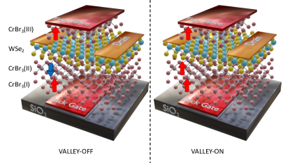
In this article, we report a giant valley splitting of 100 meV in CrBr3/WSe2/CrBr3 van der Waals trilayer heterostructure under compressive strain. The valley splitting takes place in the conduction band of WSe2 due to the hybridization with the spin-polarized bands of the CrBr3 layers. The valley splitting can be controlled through the relative orientation of the magnetization in both CrBr3 layers, leading to K, K’ , or 0 valley-polarized device. Based on that, we propose a proof-of-concept valleytronic field-effect transistor as the one depicted in Fig. 1. The top magnetic layer CrBr3(III) is pinned, while the bottom ones, CrBr3(I) and CrBr3(II), are free magnetic layers which allows to electrically control the magnetization and to turn ON/OFF the valley-polarization by a perpendicular electric field. In this proof-of-concept device, we assume that the bottom CrBr3 bilayer is grown with a monoclinic stacking which results in an antiferromagnetic (AFM) interlayer ordering. By applying an external vertical electric field, it is possible to switch the interlayer exchange between layers I and II from AFM to FM [24, 25, 26], modifying the net magnetization affecting the TMD, from 0 (OFF) to a finite value (ON). Although exfoliated samples of bilayer CrBr3 show a rhombohedral stacking with ferromagnetic interlayer magnetism, recent advances on molecular beam epitaxy (MBE) has made possible the growth of bilayer CrBr3 samples with different stacking configurations showing antiferromagnetic interlayer exchange coupling [9]. We assume that the device at source and drain is contacted with In metal, which ensures good electrons injection in the conduction band of WSe2 [27].
The manuscript is organized as follow, In section II we show the band structure of CrBr3/WSe2/CrBr3 trilayer heterostructure for different magnetic configurations using first-principles calculations. This is the region of the device where proximity effects play a key role in the development of the spin-valley splitting (the case with 4 layers is included in Appendix A). We also show the band structure for different stacking configurations to evaluate its impact on the valley splitting. In section III, we propose an easy magnetic impurity model that describes the physics taking place in the heterostructure. In section IV, we show the performance of our proposed valleytronic device in realistic multiscale transport simulations, and in section V, we summarize the results.
II First-principles calculations
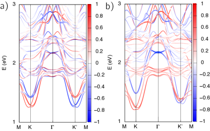
To reduce the dimension and complexity of the calculations, we have carried out first-principles calculations on the CrBr3(II)/WSe2/CrBr3(III) trilayer heterostructure with rhombohedral stacking between the layers as shown in Figure 2(a), with the W (gray) atoms lying in the hollow and bridge positions of the encapsulating CrBr3. We label this stacking RW. The unit cell is built by combining a 2x2 supercell of WSe2 with a single unit cell of the encapsulating CrBr3 layers. To make them commensurate, the WSe2 layer has been compressed 3% with respect to the standard size, while the CrBr3 layers have been stretched 0.8% with respect to the standard lattice parameter. This strain, needed to commensurate the cells and to perform feasible simulations, significantly alter the electronic structure of WSe2 moving the empty and bands below the conduction bands, as shown in Figure 2(e-g)[28, 29]. These bands, i.e. and , hybridize stronger with the empty CrBr3 bands than the leading to an unprecedented valley splitting. Therefore, strain is key for the observation of this phenomenon. The band structures have been calculated using the Quantum-Espresso ab initio package [30]. For the self-consistency, we have used fully relativistic projector augmented wave (PAW) pseudopotentials within the local density approximation (LDA), and local Hubbard (U = 4 eV) and exchange (J = 0.6 eV) corrections for the orbitals of the Cr atoms, based on previous constrained random phase approximation (cRPA) calculations [31]. The convergence threshold for the self-consistency has been set to eV, and a 8x8x1 -centered k-point grid have been used for all the cases studied. For the structure relaxation, we have included the Grimme-D2 van der Waals correction and we have let the forces relax until all the components for all the atoms in the trilayer heterostructure are smaller than Ry/Å.
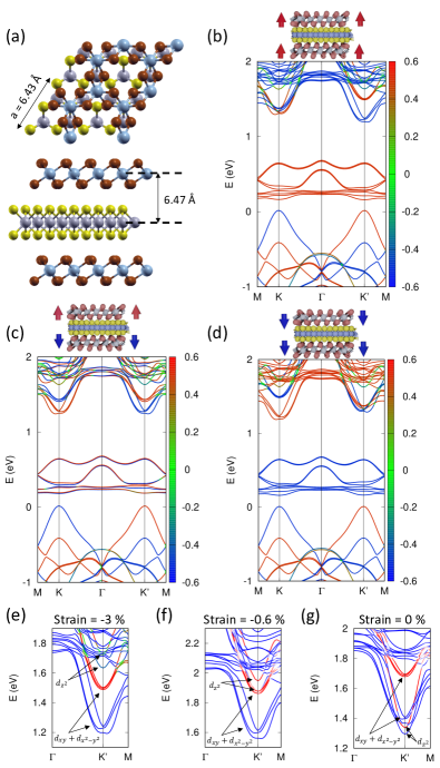
In Fig2(b-d), we show the band structures of CrBr3/WSe2/CrBr3 heterostructure for three different magnetic configurations of the CrBr3 encapsulating layers. When both CrBr3 layers are co-polarized up(down) (Fig.2(b,d)), the down(up)-spin bands from the spin-polarized Cr atoms cross above the bottom of the conduction bands of WSe2 at eV. These -bands hybridize with the down(up)-spin and bands of the WSe2 layer breaking the spin-valley symmetry and leading to a valley splitting of 100 meV. It is very important to highlight here that band alignment is mandatory to observe this large spin-valley splitting. This occurs in the case of CrBr3 and WSe2, but it is not observed when replacing CrBr3 with CrI3, or WSe2 by MoSe2 (see Appendix B). When the magnetic layers become counter-polarized, both spin-up and spin-down -bands of the Cr atom hybridize with the and bands of WSe2, restoring the valley degeneracy as in Fig.2(c).
In Figs.2(e,f,g) we report a zoom of the conduction bands of the WSe2 in the heterostructure when different percentage of compressive strain is considered (-3%, -0.6%, and 0%). As observed in the previous paragraph, strain is needed to commensurate the cells but it is also essential to move the and bands (the ones that hybridize most with CrBr3 bands) below the . We notice, however, that already for a compressive strain of -0.6% the valley splitting is present. It is important to note that the valley splitting obtained for this heterostructure is not observed if the magnetic or TMD layers are replaced (see Appendix B).
III Stacking dependent valley splitting in CrBr3/WSe2/CrBr3 heterostructure
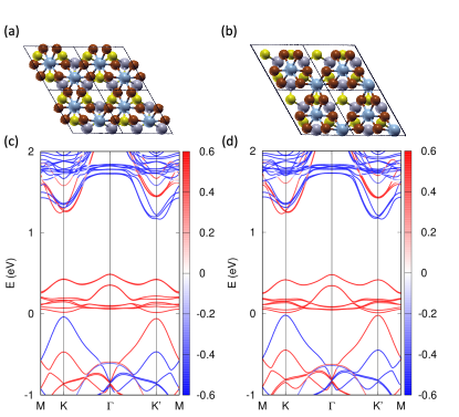
Since stacking can affect the spin-valley splitting, as previously reported [19, 20, 21], we have calculated the band structure for other two different stacking configurations. In Figs.3 (c) and (d), we show the electronic band structure for the case in which the stacking configuration between layers is monoclinic (M) and the case in which the stacking is rhombohedral, like the one reported in the previous Section, but the hollow sites are occupied by Se atoms (RSe). The structural details are reported in Figs.3 (a) and (b) for the two stackings respectively. We compare these two stackings with the one (RW) reported in the previous Section, i.e. rhombohedral with the W atoms appearing in the hollow sites of the Cr hexagonal lattices, in terms of ground-state energy, valley splitting in the conduction and valence band of the WSe2. In this stacking (RW) the valley splitting is the higher of the three cases studied (101 meV), while the valley splitting in the valence band is lower than 1 eV and the energy is meV above the stacking (M), which is the one with the lowest energy. In the monoclinic stacking the valley splitting in the conduction band decreases to 79 meV, however, this is the only case where strong valley splitting is observed in the valence band (21 meV). Finally, we discuss stacking (RSe). This is the stacking with the higher energy. It gives rise to the smaller valley splitting in the conduction band (67 meV). Similar to the RW stacking, the valley splitting in the valence bands is lower than 1 meV. These results demonstrate that the change in the stacking affects the hybridization of the -orbitals in different layers (which is the main mechanism of valley polarization) leading to different values of the valley splitting. These results are summurized in Table 1. More importantly, in all cases a valley splitting is observed higher than 60 meV making this heterostructure a promising candidate for future valleytronic proof-of-concept devices.
| (meV) | (meV) | (meV) | |
|---|---|---|---|
| RW | 97 | 101 | 1 |
| M | 0 | 79 | 21 |
| RSe | 343 | 67 | 1 |
IV Model and theoretical description
The results shown in Fig.2 clearly highlight the importance of 2D magnetic materials in the design of future TMD-based van der Waals valleytronic devices. To better understand the physics underlying these results, and to give a prospect for the future design of van der Waals valleytronics, we use a toy model that contains the most important interactions giving rise to this big valley splitting. As a first approach to our valley-polarized device, we use a single-orbital tight-binding model in an hexagonal lattice with broken sublattice symmetry and spin-orbit coupling (SOC) to describe the electrons in the TMD. The encapsulating magnetic layers are described using two magnetic impurities which couple to the TMD with different magnetic configurations (see insets in Fig. 4). Although CrBr3 is a periodic two-dimensional material, the -bands of the Cr atoms involved in the valley splitting are almost dispersionless due to the small hopping between neighboring magnetic atoms. This justifies the use of magnetic impurities instead of a more realistic magnetic 2D material. The model Hamiltonian describing the van der Waals heterostructure is given by
| (1) | |||||
the first two terms describe electrons in a gapped hexagonal lattice, where is the sublattice index, is the mass term which opens up a gap in the band structure, is the hopping term between neighbouring sites in the honeycomb lattice, and are the creation and annihilation operators acting on each site of the hexagonal lattice. The third term introduces the spin-orbit Rashba coupling () which is essential to couple spin and valley, with the vector of Pauli matrices, the unit vector connecting first neighbours in the honeycomb lattice, and the unit cartesian vector along the -direction. The fourth term is the intrinsic spin-orbit coupling (), with and the two vectors connecting second-neighbor sites . The fifth term includes the on-site energy () and exchange interaction () for the magnetic layers where the sign controls the spin polarization, down or up, in the impurity. is the -component of the Pauli matrix vector, and creates and annihilates an electron in the impurity sites. The last term allows to tune the hopping between the magnetic layers and the hexagonal lattice ().
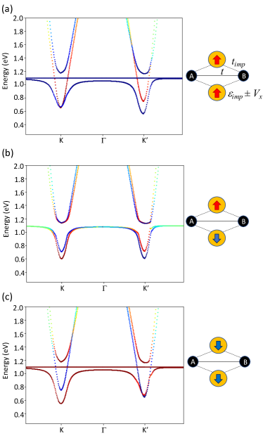
In Fig.4, we show the evolution of the valleys in the bottom of the conduction band of the TMD for different magnetic configurations of the magnetic layers. To model the FM/TMD/FM heterostructure we have used the Hamiltonian in Eq.1 with eV, eV, eV, eV, eV, eV, and eV (for more details, see Appendix C). When the magnetic layers are co-polarized, an almost flat band from the CrBr3 magnetic layers crosses the conduction bands of the TMD and hybridizes with the bands of the same spin, breaking the spin-valley symmetry and inducing a valley polarization that depends on the spin sign. Since the conduction bands in the model are mostly localized in the A-sublattice, , the two impurities, i.e. magnetic layers, couple stronger to the A sites than to the B sites, leading to a weakly coupled flat band in the energy dispersion, as shown in Fig.4(a,c). For spin up(down), the TMD is K’(K)-polarized with a valley splitting of around meV as shown in Figs.4(a,c). When both magnetic layers are counter-polarized, spin up and down bands of the TMD are hybridized with the flat impurity bands, which eventually restores the spin-valley symmetry leading to a 0-polarized TMD as shown in Figs.4 (b). Therefore, finding the correct combination of a TMD and a 2D magnetic semiconductor it is possible to efficiently break the spin-valley symmetry in the TMD leading to unexpectedly high values of valley splitting.
V Multi-scale transport simulations.
In order to precisely quantify and assess the potential performances of the proposed devices we perform precise multi-scale transport simulations. Upon the DFT simulation we perform the so-called wannierization to transform the Hamiltonian expressed in terms of plane-waves to maximally localized Wannier functions through the use of the Wannier90 code [32]. The wannierization is performed projecting on the of the W atoms and on the of the Cr atoms of each layer, selecting as frozen window the energy range from 1.15 eV till 1.45 eV. In Fig.5 we report the spin-polarized band structure obtained after performing the wannierization for the counter polarized (a) and co-polarized-down (b) heterostructres. It’s worth noting that this wannierization choice allows to retain an excellent accuracy on the spin-polarized band structure while selecting only the energy window of interest for transport.
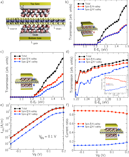
The simulated device is schematically reported in Fig.6(a), where we have considered as source and drain a region of monolayer WSe2 while the channel is composed of CrBr3/WSe2/CrBr3 heterostructure. Double (top and bottom) gate configuration is considered in the channel region, with an oxide between the gates and the channel material of 0.5 nm thickness and 3.9 relative dielectric constant. The channel length is 5.8 nm as well as the source and drain regions. In the source and drain contacts we have assume a doping of 5 x molar fraction. In order to define the source and drain region with only WSe2 monolayer, we have used the Wannier Hamiltonian obtained for the counter polarized structure in Fig.5(a), following the procedure described in Ref. [33], i.e. selecting from the heterostructure Hamiltonian only the sub-Hamiltonian belonging to the WSe2 layer. We have ensured that the Hamiltonian of WSe2 obtained from the procedure described in Ref. [33] is equal to the WSe2 isolated monolayer. To ensure correct band allignment between source/drain and channel region, we have shift the onsite energies source and drain WSe2 Hamiltonian of 70 meV. The energy shift has been calculated following the procedure described in Ref. [34]. In Figs.6(b,c) we report the transmission coefficient around the minimum of the WSe2 conduction band for flat potential while considering in the channel region counter-polarized, Fig.6(b), and co-polarized-down, Fig.6(c), channel. We can observe that in the first case the total transmission is equally composed of both spin- (K-valley) and spin- (K’-valley) component, while in the case of co-polarized CrBr3 layers we observe higher transmission for the spin- (K-valley) component. To better visualise it, we provide a zoom close to the bottom of the conduction band in Fig.6(d). In the inset, we show the transmission ratio in the same energy range, where it is observed that the spin-/K-valley contributes 80-60 of the total transmission. Finally, we perform fully transport simulations of the device solving self-consistently non-equilibrium Green’s functions and the Poisson equation using NanoTCAD ViDES sofware [35, 36]. In Fig.6(e) we report the transfer characteristic of the device while applying gate voltages from -0.15 V till 0.2 V and fixing a source-to-drain voltage of 0.1 V. We can observe that the device switch OFF/ON while maintaining a predominance of spin-/K-valley current component. To quantify the degree of spin/valley current polarization we have computed the current ratio in Fig.6(f), where we can observe that in the operation range considered the current spin/valley polarization is always higher than 80.
VI Conclusions
In this work, we have shown by means of DFT and transport simulations the possibility to engineer valleytronic devices out of van der Waals magnetic heterostructures combining TMDs and 2D magnetic materials. In the particular case studied, namely CrBr3/WSe2/CrBr3 trilayer, we find a giant valley splitting of the order of 100 meV in the conduction band of the TMD under compressive strain due to the hybridization of the bands of CrBr3 with the empty and bands of WSe2. The transport simulations based on DFT show a valley polarization of the injected current that remains for gate voltage range of 0.3 V. This work lays the foundations for the future design of valleytronic devices based on van der Waals heterostructures.
Acknowledgments
D.S. acknowledges financial support from Generalitat Valenciana through the CIDEGENT program (Nr. CIDEGENT/2021/052). This study forms part of the Advanced Materials program and was supported by MCIN with funding from European Union NextGenerationEU (PRTR-C17.I1) and by Generalitat Valenciana (MFA/2022/045). The authors gratefully acknowledge Italian Ministry of University and Research (MUR) PRIN project SECSY (2022FPAKWF) and CN00000013 National Centre for HPC, Big Data and Quantum Computing (HPC).
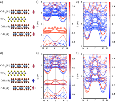
Appendix A Spin-valley splitting in Bilayer-CrBr3/WSe2/CrBr3 heterostructure and effect of perpendicular electric field
The proof-of-principle device reported in Fig.1 is made of WSe2-layer encapsulated on top by a monolayer CrBr3 and on bottom by a bilayer of CrBr3 in the monoclinic stacking and relies on the possibility of switching the interlayer magnetic order of layer I and II by the top and bootom gate. Nevertheless, in the subsequent calculations we have focused our attention on the top three layers, where the proximity effects play a key role, and we have assumed that the electric field produced by the gates do not alter the valley splitting. In the present Appendix we justify both assumptions.
Firstly, we have fully relaxed the bilayer-CrBr3/WSe2/CrBr3 heterostructre, with the same parameters reported in the main text. We have observed that the CrBr3 (II) layer is slightly closer to the WSe2 layer (0.007 nm) respect to the top layer. To demonstrate the negligible influence of the first bottom layer (CrBr3 (I)) on the valley-splitting of the WSe2 conduction band, in Fig.7(b) we report the spin-projected band structure and a zoom (Fig.7(c)) near the bottom of the conduction band of the WSe2 for the co-polarized structure reported in Fig.7(a). We observe that the valley splitting is preserved, if not slightly enhanced (we measure a splitting of 107 meV): the enhancement is mainly due to the fact that the CrBr3 (II) is closer to the WSe2 layer. In Fig.7(e) we report the band structure and the zoom (Fig.7(f)) near the bottom of the conduction band of the four-layers structure but with the CrBr3 layers (II) and (III) counter-polarized. In this case, no valley-splitting is observed, so the bottom layer CrBr3 (I), also for this configuration, does not alter the bottom of the conduction band of the WSe2.
Once we have verify that the bottom CrBr3 (I) does not influence the valley splitting, we have carried out a DFT calculation on the trilayer heterostructure in order to discard detrimental effects on the valley splitting due to the electric field produced by the gates. In particular we have considered a perpendicular electric field = 0.8 V/nm. The results are shown in Fig.8.
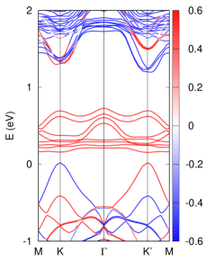
In Fig.8 we clearly see how the electric field splits the bands of the CrBr3 over the Fermi energy. However, the valley splitting in the conduction band is not affected by the electric field and remains almost of the same value (99 meV). Since the empty bands of the CrBr3 layers crossing the conduction band of WSe2 are not strongly affected by the electric field, the hybridization between -bands is maintained, leading to the same valley splitting even in presence of the electric field.
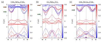
Appendix B Spin-valley splitting in other heterostructures
To highlight the importance of the band alignment and spin-orbit coupling on the spin-valley splitting mechanism in magnetic van der Waals heterostructures, in Fig.9 we have compared electronic structure of the CrBr3/WSe2/CrBr3 heterostructure with other two heterostructures, namely CrI3/WSe2/CrI3 and CrBr3/MoSe2/CrBr3. In this figure, it is possible to compare the position of the bands of the magnetic layers (orange arrow) with respect to the bottom of the conduction band of the TMD (green arrow). The spin-valley splitting in the conduction band is only observed for the case of CrBr3/WSe2/CrBr3 due to the proximity of the bands of the CrBr3 to the bottom of the conduction band of WSe2. In the case of CrBr3/MoSe2/CrBr3, although the alignment is good, the lower spin-orbit coupling (clearly denoted by the smaller splitting in the valence bands compared with WSe2) reduces the valley splitting. It is interesting to observe in this case that in both K and K’ the conduction bands are polarized down (blue color) in contrast to the other two cases.
Appendix C Single-orbital tight-binding model of a magnetically-encapsulated transition metal dichalcogenide
Several parameters are involved in the description of the electronic structure of a magnetically-encapsulated transition metal dichalcogenide (TMD). In this SI, we focus first on the effect of the Rashba splitting () and the intrinsic spin-orbit coupling () to properly tune the spin-splitting and the expectation value of the off-plane spin operator of the TMD conduction bands. Then, we show how the intensity of the exchange interaction of the ferromagnets (FM) affects the electronic structure of the TMD for a constant FM-TMD interaction. Finally, we study the tunability of the valley splitting for different values of the FM-TMD interaction.
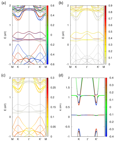
Spin-orbit coupling ( and ). In Fig.10(a), we show the spin-projected bands of the CrBr3/WSe2/CrBr3 heterostructure with antiferromagnetically(AFM)-aligned magnetic layers. This is the starting point for our tight-binding model (Fig.10(d)). It shows the typical gapped TMD band structure with the two valleys at K and K’, the high spin splitting in the valence bands, and the small spin-splitting in the conduction bands (spin up and down bands are plotted in red and blue respectively). On top of the TMD band structure, it is possible to see several flat bands crossing at around eV above the bottom of the conduction bands of WSe2 belonging to the CrBr3 layers. These bands can be easily observed in the band projections shown in Fig.10(b,c) around eV at the -point.
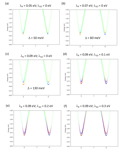
The measured spin-splitting in the conduction bands of the WSe2 with AFM-aligned magnetic layers is of the order of meV, much higher than previously reported values [37]. In Fig.11(a-c), we show the evolution of the conduction band of the TMD for different values of the Rashba splitting using the tight-binding model in Eq. 1 of the main manuscript. For meV, we find a splitting of meV, very similar to the DFT result. The intrinsic spin-orbit coupling has important implications in the spin texture around the valleys and competes with the Rashba SOC [38]. While the Rashba coupling contributes to a more planar and helical spin texture around the valleys, the intrinsic spin-orbit coupling tends to align the spins along the off-plane direction. In Fig.11(d-f), we show how the in-plane contribution (green dots) is reduced along the K--K’ path for increasing values of the intrinsic spin-orbit coupling, and the bands become up (red) and down (blue) spin-polarized. As shown in Fig.10(a), the valence and conduction bands of the TMD are mostly off-plane polarized with a very small in-plane contribution. In our model, we find this situation for meV, which is close to the reported atomic spin-orbit coupling of the Se atom meV [39].
Exchange interaction (). Exchange interaction is a key ingredient, together with SOC, to realize a valley splitting. In our heterostructure, the exchange field comes from the CrBr3 encapsulated layers. When the magnetization is turned on, the bands split eV, as shown in Fig.12(a) for the AFM case. In our model, we have located the impurity band at the bottom of the conduction band eV with an exchange interaction eV (see Fig.12(b)).
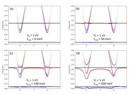
FM-TMD interaction (). Finally, we focus on the interlayer coupling between the ferromagnetic encapsulating layers and the TMD. The interaction between the orbitals located at different layers is crucial for the observation of a valley polarization. In Fig.12(b-d), we show the evolution of valley splitting for three different interlayer hopping parameter, namely, , , and meV. To have a more clear picture of the evolution of the valley splitting with the interlayer hopping, we have calculated the splitting for several values of the interlayer hopping (see Fig.13). For meV the evolution is parabolic , and then saturates for meV.
References
- Cao et al. [2018] Y. Cao, V. Fatemi, S. Fang, K. Watanabe, T. Taniguchi, E. Kaxiras, and P. Jarillo-Herrero, Unconventional superconductivity in magic-angle graphene superlattices, Nature 556, 43 (2018).
- Song et al. [2018] K. Song, D. Soriano, A. W. Cummings, R. Robles, P. Ordejón, and S. Roche, Spin proximity effects in graphene/topological insulator heterostructures, Nano Letters 18, 2033 (2018).
- Karpiak et al. [2019] B. Karpiak, A. W. Cummings, K. Zollner, M. Vila, D. Khokhriakov, A. M. Hoque, A. Dankert, P. Svedlindh, J. Fabian, S. Roche, and S. P. Dash, Magnetic proximity in a van der waals heterostructure of magnetic insulator and graphene, 2D Materials 7, 015026 (2019).
- Zhong et al. [2020] D. Zhong, K. L. Seyler, X. Linpeng, N. P. Wilson, T. Taniguchi, K. Watanabe, M. A. McGuire, K.-M. C. Fu, D. Xiao, W. Yao, and X. Xu, Layer-resolved magnetic proximity effect in van der waals heterostructures, Nature Nanotechnology 15, 187 (2020).
- Kezilebieke et al. [2020] S. Kezilebieke, M. Nurul Huda, V. Vaňo, M. Aapro, S. C. Ganguli, O. J. Silveira, S. Głodzik, A. S. Foster, T. Ojanen, and P. Liljeroth, Topological superconductivity in a van der Waals heterostructure, Nature 588, 424 (2020).
- Lyons et al. [2020] T. P. Lyons, D. Gillard, A. Molina-Sánchez, A. Misra, F. Withers, P. S. Keatley, A. Kozikov, T. Taniguchi, K. Watanabe, K. S. Novoselov, J. Fernández-Rossier, and A. I. Tartakovskii, Interplay between spin proximity effect and charge-dependent exciton dynamics in MoSe2/CrBr3 van der Waals heterostructures, Nat. Commun. 11, 6021 (2020).
- Gong et al. [2017] C. Gong, L. Li, Z. Li, H. Ji, A. Stern, Y. Xia, T. Cao, W. Bao, C. Wang, Y. Wang, Z. Q. Qiu, R. J. Cava, S. G. Louie, J. Xia, and X. Zhang, Discovery of intrinsic ferromagnetism in two-dimensional van der waals crystals, Nature 546, 265 (2017).
- Huang et al. [2017] B. Huang, G. Clark, E. Navarro-Moratalla, D. R. Klein, R. Cheng, K. L. Seyler, D. Zhong, E. Schmidgall, M. A. McGuire, D. H. Cobden, W. Yao, D. Xiao, P. Jarillo-Herrero, and X. Xu, Layer-dependent ferromagnetism in a van der waals crystal down to the monolayer limit, Nature 546, 270 (2017).
- Chen et al. [2019] W. Chen, Z. Sun, Z. Wang, L. Gu, X. Xu, S. Wu, and C. Gao, Direct observation of van der waals stacking dependent interlayer magnetism, Science 366, 983 (2019).
- Och et al. [2021] M. Och, M.-B. Martin, B. Dlubak, P. Seneor, and C. Mattevi, Synthesis of emerging 2d layered magnetic materials, Nanoscale 13, 2157 (2021).
- Gibertini et al. [2019] M. Gibertini, M. Koperski, A. F. Morpurgo, and K. S. Novoselov, Magnetic 2d materials and heterostructures, Nat. Nanotech. 14, 408 (2019).
- Soriano et al. [2019] D. Soriano, M. I. Katsnelson, and J. Fernández-Rossier, Magnetic two-dimensional chromium trihalides: A theoretical perspective, Nano Letters 20, 6225 (2019).
- Klein et al. [2018] D. R. Klein, D. MacNeill, J. L. Lado, D. Soriano, E. Navarro-Moratalla, K. Watanabe, T. Taniguchi, S. Manni, P. Canfield, J. Fernández-Rossier, and P. Jarillo-Herrero, Probing magnetism in 2D van der Waals crystalline insulators via electron tunneling, Science 360, 1218 (2018).
- Ghazaryan et al. [2018] D. Ghazaryan, M. T. Greenaway, Z. Wang, V. H. Guarochico-Moreira, I. J. Vera-Marun, J. Yin, Y. Liao, S. V. Morozov, O. Kristanovski, A. I. Lichtenstein, M. I. Katsnelson, F. Withers, A. Mishchenko, L. Eaves, A. K. Geim, K. S. Novoselov, and A. Misra, Magnon-assisted tunnelling in van der Waals heterostructures based on CrBr3, Nat. Electron. 1, 344 (2018).
- Wang et al. [2018] Z. Wang, I. Gutiérrez-Lezama, N. Ubrig, M. Kroner, M. Gibertini, T. Taniguchi, K. Watanabe, A. Imamoğlu, E. Giannini, and A. F. Morpurgo, Very large tunneling magnetoresistance in layered magnetic semiconductor cri3, Nature Communications 9, 2516 (2018).
- Ai et al. [2021] L. Ai, E. Zhang, J. Yang, X. Xie, Y. Yang, Z. Jia, Y. Zhang, S. Liu, Z. Li, P. Leng, X. Cao, X. Sun, T. Zhang, X. Kou, Z. Han, F. Xiu, and S. Dong, Van der waals ferromagnetic josephson junctions, Nature Communications 12, 6580 (2021).
- Wu et al. [2020] Y. Wu, S. Zhang, J. Zhang, W. Wang, Y. L. Zhu, J. Hu, G. Yin, K. Wong, C. Fang, C. Wan, X. Han, Q. Shao, T. Taniguchi, K. Watanabe, J. Zang, Z. Mao, X. Zhang, and K. L. Wang, Néel-type skyrmion in wte2/fe3gete2 van der waals heterostructure, Nature Communications 11, 3860 (2020).
- Zhong et al. [2017] D. Zhong, K. L. Seyler, X. Linpeng, R. Cheng, N. Sivadas, B. Huang, E. Schmidgall, T. Taniguchi, K. Watanabe, M. A. McGuire, W. Yao, D. Xiao, K.-M. C. Fu, and X. Xu, Van der waals engineering of ferromagnetic semiconductor heterostructures for spin and valleytronics, Science Advances 3, e1603113 (2017).
- Zhang et al. [2019] Z. Zhang, X. Ni, H. Huang, L. Hu, and F. Liu, Valley splitting in the van der waals heterostructure : The role of atom superposition, Phys. Rev. B 99, 115441 (2019).
- Ge et al. [2022] M. Ge, H. Wang, J. Wu, C. Si, J. Zhang, and S. Zhang, Enhanced valley splitting of wse2 in twisted van der waals wse2/cri3 heterostructures, npj Computational Materials 8, 32 (2022).
- Zollner et al. [2023] K. Zollner, P. E. Faria Junior, and J. Fabian, Strong manipulation of the valley splitting upon twisting and gating in and van der waals heterostructures, Phys. Rev. B 107, 035112 (2023).
- Ciorciaro et al. [2020] L. Ciorciaro, M. Kroner, K. Watanabe, T. Taniguchi, and A. Imamoglu, Observation of magnetic proximity effect using resonant optical spectroscopy of an electrically tunable heterostructure, Phys. Rev. Lett. 124, 197401 (2020).
- Choi et al. [2023] J. Choi, C. Lane, J.-X. Zhu, and S. A. Crooker, Asymmetric magnetic proximity interactions in mose2/crbr3 van der waals heterostructures, Nature Materials 22, 305 (2023).
- Jiang et al. [2018a] S. Jiang, L. Li, Z. Wang, K. F. Mak, and J. Shan, Controlling magnetism in 2D CrI3 by electrostatic doping, Nat. Nanotech. 13, 549 (2018a).
- Jiang et al. [2018b] S. Jiang, J. Shan, and K. F. Mak, Electric-field switching of two-dimensional van der waals magnets, Nat. Mater. 17, 406 (2018b).
- Huang et al. [2018] B. Huang, G. Clark, D. R. Klein, D. MacNeill, E. Navarro-Moratalla, K. L. Seyler, N. Wilson, M. A. McGuire, D. H. Cobden, D. Xiao, W. Yao, P. Jarillo-Herrero, and X. Xu, Electrical control of 2D magnetism in bilayer CrI3, Nat. Nanotech. 13, 544 (2018).
- Liu et al. [2013] W. Liu, J. Kang, D. Sarkar, Y. Khatami, D. Jena, and K. Banerjee, Role of metal contacts in designing high-performance monolayer n-type wse2 field effect transistors, Nano Letters 13, 1983 (2013), pMID: 23527483, https://doi.org/10.1021/nl304777e .
- Deng et al. [2018] S. Deng, L. Li, and M. Li, Stability of direct band gap under mechanical strains for monolayer mos2, mose2, ws2 and wse2, Physica E: Low-dimensional Systems and Nanostructures 101, 44 (2018).
- Sohier et al. [2023] T. Sohier, P. M. M. C. de Melo, Z. Zanolli, and M. J. Verstraete, The impact of valley profile on the mobility and kerr rotation of transition metal dichalcogenides, 2D Mater. 10, 025006 (2023).
- et al. [2009] P. G. et al., Quantum espresso: a modular and open-source software project for quantum simulations of materials, Journal of Physics: Condensed Matter 21, 395502 (2009).
- Soriano et al. [2021] D. Soriano, A. N. Rudenko, M. I. Katsnelson, and M. Rösner, Environmental screening and ligand-field effects to magnetism in cri3 monolayer, npj Computational Materials 7, 162 (2021).
- Mostofi et al. [2008] A. A. Mostofi, J. R. Yates, Y.-S. Lee, I. Souza, D. Vanderbilt, and N. Marzari, wannier90: A tool for obtaining maximally-localised Wannier functions, Comp. Phys. Commun. 178, 685 (2008).
- Cannavò et al. [2021] E. Cannavò, D. Marian, E. G. Marín, G. Iannaccone, and G. Fiori, Transport properties in partially overlapping van der waals junctions through a multiscale investigation, Phys. Rev. B 104, 085433 (2021).
- Katagiri et al. [2016] Y. Katagiri, T. Nakamura, A. Ishii, C. Ohata, M. Hasegawa, S. Katsumoto, T. Cusati, A. Fortunelli, G. Iannaccone, G. Fiori, S. Roche, and J. Haruyama, Gate-tunable atomically thin lateral mos2 schottky junction patterned by electron beam, Nano Letters 16, 3788 (2016), pMID: 27152475, https://doi.org/10.1021/acs.nanolett.6b01186 .
- [35] NanoTCAD ViDES, Available at: http://vides.nanotcad.com/vides/.
- Marian et al. [2023] D. Marian, E. G. Marin, M. Perucchini, G. Iannaccone, and G. Fiori, Multi-scale simulations of two dimensional material based devices: the nanotcad vides suite, Journal of Computational Electronics 10.1007/s10825-023-02048-2 (2023), cited by: 1; All Open Access, Hybrid Gold Open Access.
- Kośmider et al. [2013] K. Kośmider, J. W. González, and J. Fernández-Rossier, Large spin splitting in the conduction band of transition metal dichalcogenide monolayers, Phys. Rev. B 88, 245436 (2013).
- Cummings et al. [2017] A. W. Cummings, J. H. Garcia, J. Fabian, and S. Roche, Giant spin lifetime anisotropy in graphene induced by proximity effects, Phys. Rev. Lett. 119, 206601 (2017).
- Wittel and Manne [1974] K. Wittel and R. Manne, Atomic spin-orbit interaction parameters from spectral data for 19 elements, Theoretica chimica acta 33, 347 (1974).