Electronic structure and conductivity in functionalized multi-layer Black Phosphorene
Abstract
Phosphorene and its components are highly reactive to oxygen when exposed to ambient conditions due to the presence of lone pairs of electrons on phosphorus atoms. Functionalization serves as a solution to prevent the chemical degradation of these materials. In this study, we investigate the impact of a rather strong covalent or non-covalent functionalization of phosphorene (monolayer Black Phosphorus (BP)), few-layer BP, and bulk BP. We use an effective tight-binding Hamiltonian that corresponds to one orbital per site, for which covalent functionalization is simulated by atomic vacancies, and non-covalent functionalization is simulated by Anderson disorder. We show that these two types of functionalisation act differently on the electronic structure and quantum diffusion, in particular on gap and mobility gap for a high degree of functionalisation.
I Introduction
The scientific community shows now keen interest in two-dimensional (2D) materials, focusing on their potential applications in electronics, sensing, dye degradation, and various biomedical uses [1, 2, 3, 4]. The first 2D crystal realized by mechanical exfoliation was graphene in 2004. It was an interesting material for its outstanding electronic and mechanical properties. However, its zero band gap limited its use in optoelectronics and semiconductor devices. Therefore, several researches have been carried out to find other 2D materials with a band gap and large carrier mobility to replace the graphene. In 2014, a successful exfoliation of few Black Phosphorus (BP) layers, the most stable allotrope of Phosphorus, was realized, and phosphorene, i.e. monolayer black phosphorus, was obtained [5, 6, 7]. In contrast to graphene, phosphorene is a 2D semiconductor with a direct band gap with a high hole mobility up to 1000 cm2V-1s-1 at room temperature [8]. Its band gap varies from 2 eV [9] for phosphorene monolayer to 0.3 eV for the bulk [10] and it has unique in-plane anisotropy properties. Functionalization or disorder can modify the band gap value to tailor these materials for desired applications. Phosphorene and its components are highly sensitive to the environment. This sensitivity arises from their pronounced reactivity to oxygen under ambient conditions, which may constrain their practical use in real devices. Therefore, it is crucial to investigate the impact of defects and impurities on electronic structure and transport properties for this purpose [11].
Several recent experiments have been carried out recently to protect few-layer BP from chemical degradation due to environment, and to tailor its electrical properties. Covalent and non-covalent functionalization have been realized experimentally to enhance its environmental stability [12, 13, 14, 15, 16, 17]. The lone pair electrons of phosphorus atoms create a chemical bond with the adatoms. Additionally, theoretical investigations have contributed to develop the chemistry of few-layer BP using DFT models [18, 19, 20]. Yet crucial aspects of its reactivity remain largely unexplored and there is a lack of consensus between different interpretations of the experimental results. Functionalization can be realized on the surface of few-layer BP or of phosphorene but it can also be randomly distributed among the layers [21, 22]. It has also been demonstrated that functionalization can be covalent with resonant scatterers, such as functional groups containing free radicals like hydrogen, halogens, hydroxyl, thiol groups, and organic substituents which are important for biological applications [23, 11]. Functionalization can also be non covalent with non-resonant scatterers such as cesium, potassium or some organic molecules based on Van der Waals interaction [21, 24, 25, 26].
In this paper, we focus our study on the electronic structure and the conductivity of functionalized monolayer, few-layer BP, and bulk by using the tight-binding (TB) model developed by Rudenko et al. [27, 28]. In the case of graphene, the description of its electronic properties at low energy is very simple because it is performed by the TB Hamiltonian involving only one hopping parameter. But for phosphorene, the use of this method is very complicated because it has four orbitals per atom and we must take into account the mixture of states of different symmetries. We model covalent functionalization using vacancies and non-covalent functionalization through Anderson disorder. We discuss the effects of these types of adsorbates on the density of States (DOS), conductivity, and mobility in phosphorene, few layers of black phosphorus (BP), and the bulk. Our idea is to compare the effect depending on the number of phosphorus layers, the concentration of adatoms, and the nature of the functionalization and try to emphasize the anisotropy of the material. In contrast to other theoretical research conducted through DFT calculations [3, 29, 30] and tight-binding Hamiltonian method [31], our research stands out by its unique emphasis on exploring transport properties. Specifically, we delve into the impacts of both covalent and non-covalent functionalization, particularly under conditions of high disorder where the Boltzmann semi-classical approach is not applicable.
The paper is organized as follows. The atomic structure and the TB Hamiltonian are presented in Sec. II. In Sect. III, the numerical method for transport calculation is briefly detailed as well as the calculated transport coefficients. Results for resonant scatterers and non-resonant scatterers are presented in Sec. IV.1 and IV.2, respectively. Sec. V is dedicated to the discussion and conclusion. Additional figures are shown in the Supplemental Material [32].
II Phosphorene structure and effective Hamiltonian
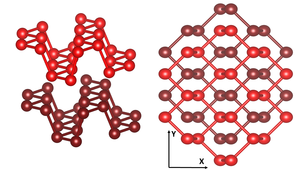
In phosphorene, phosphorus atoms are joined by covalent bonds with bond angles of 96.34∘ and 103.09∘ [21, 22] (FIG. 1). The intralayer bonding results from the hybridization of P atoms, giving rise to three bonding orbitals per two atoms augmented by lone pairs associated with each atom. It results in a strong stability in crystal structure because these angles are close to perfect tetragonal ones. The bonds out of the plane have an angle of approximately 45∘ with respect to the plane and are responsible for the puckered structure of phosphorene in contrast with graphene and 2D metal chalcogenides. The two first neighbor atoms in the plane are at the distances 2.224 Å, and the third neighbor one out of the plane is at 2.244 Å. The crystal structure of black phosphorus is orthorhombic with the lattice parameters 4.376, 3.314 and 10.478 Å for , , and respectively [33]. In the phosphorene, the primitive cell contains four atoms at positions and with and . The puckered honeycomb lattice formed by covalently bounded phosphorus atoms results in a significant in-plane anisotropy, similar to bulk phosphorus (BP), which distinguishes it from many other isotropic 2D materials [34, 35]. This anisotropy has implications for electronic properties of phosphorene such as an energy band structure, a density of states, a conductivity, etc… [36, 10, 37, 38]. The -axis is the armchair direction and the one is the zigzag direction (FIG. 1).
To study the effect of random disorder one needs to perform numerical calculations in a supercell containing several hundred thousand atoms. That can be only done in a framework of a tight binding (TB) Hamiltonian. However, in contrast to graphene which involves only one hopping parameter between orbitals, the phosphorene cell has four atoms with four orbitals per atom, , , and , that need to be considered. The exact modeling of the TB Hamiltonian is a challenge because of the mixture of the orbital and orbitals . However, it was been shown [39, 40, 27] that the orbital has a large contribution to the valence and conduction band around the band gap and its role is predominant compared to the roles of the other orbitals , and . Therefore, following Rudenko et al. [27, 28], it is possible to consider only one orbital per atom that looks like a without being exactly the orbital. This approximation is reasonable as long as the energy is fairly close to the gap.
Indeed this effective model has been successfully used to describe the studies that concern phosphorene nanoribbons [41, 42, 43], electric [41, 44] and magnetic fields [45, 31, 46], field-effect electronic devices [5] and quantum dots [47]. We also use that effective TB model which corresponds to one orbital per P site [28],
| (1) |
where is the orbital located at and the sum runs over neighboring , lattices sites. is the on-site energy of the electron and it takes the same value for all sites because we suppose that all sites are equivalent. () is the intralayer (interlayer) hopping parameter between the and sites. Those parameters are obtained [28] by the construction of a set of four maximally localized Wannier functions corresponding to -like orbitals from DFT calculation with quasiparticle GW approximation [28]. Typically, we use the TB parameters proposed by Rudenko et al. in Ref. [28]: ten intralayer and four interlayer hopping parameters over the distances between the corresponding interacting sites up to 5.5 Å.
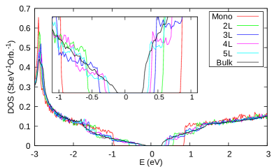
FIG. 2 shows the total densities of states (DOS) for multilayer of BP (from monolayer to bulk). One can see that the band gap of the monolayer is about 1.75 eV. The origin of this gap is the fact that this TB Hamiltonian involved the nearest neighbor atoms, two in-plane hopping terms eV and one out-of-plane hopping term eV. The distinct sign of in comparison to implies the opening of the gap [27, 28, 48]. It should be noted that more theoretical works have predicted a value energy gap ranging from eV [6, 10, 49] up to eV [9] depending on the calculation method, and the measured value experimentally is around 2 eV [50, 51].
The band gap decreases according to the number of layers and for the bulk the calculated value is around 0.3 eV. A step-like behavior is the signature of reducing dimensionally.
III Numerical method for transport
The electronic properties of the multilayer of phosphorene are calculated by using the real space Kubo Greenwood formalism computed by recursion and polynomial expansion method [52, 53, 54, 55, 56]. It allows us to compute efficiently quantum transport in a large system for which calculation by diagonalization is not numerically feasible. This formalism has been used to study the effect of vacancies, defects and disorder on quantum transport in different materials such as graphene monolayer and bilayer [57, 58, 59, 60, 61, 62, 63], carbon nanotube [64, 65, 66], quasicristals [56], perovskites [67], etc…
This real space method allows the include local defects directly into the Hamiltonian, and it allows a random distribution of defects in the huge supercell.
To make a systematic study of the effect of defects on the electronic properties, we study two types of generic defects:
(i) Resonant defect, i.e. defect that creates a covalent bond with a P atom of the phosphorene.
As the system is described by the effective four-band Hamiltonian, with one -like orbital per phosphorus atom, we use the same approach as in the case of graphene to model resonant scatterers [59, 57, 58].
Indeed an adatom or ad-molecule bound covalently with the P atom is almost equivalent for the electron bands to remove the corresponding orbitals of the bounded P. Thus a resonant scatter is modelized by a vacant P atom. In our calculation defects (vacancies) are
randomly over the whole supercell of 640 000 P atoms per layer.
(ii) Non-resonant defect, i.e. non-covalent functionalization, such as Van der Waals bonding, that creates a small local perturbation of the electronic structure.
A common method of dealing with this type of defect is to use the Anderson disorder where the on-site P energies (equation (1)) are randomly distributed in
. is the magnitude of that disorder and the on-site energy of the orbital without disorder from Ref. [28].
To evaluate the effect of the anisotropy of phosphorene on the conductivity , we compute [52, 53, 54, 55, 56] and , which are the average square of the quantum spreading along the armchair direction and the zigzag direction, respectively (FIG. 1), after a time and for states at energy .
In such a calculation, all quantum effects –including all multiple-scattering effects– are taken into account to calculate the average square spreading without inelastic scattering i.e. at zero temperature. At finite temperature , the inelastic scattering caused by the electron-phonon interactions is implanted by using the Relaxation Time Approximation (RTA)[59]. The conductivity in the -direction (-direction) is thus given by,
| (2) | |||||
| (3) | |||||
| (4) |
where is the Fermi energy, is the inelastic scattering time, is the total density of states (total DOS), the diffusivity along the -axis (-axis), and is the inelastic mean free path. is the typical distance of propagation during the time interval for electrons at energy . Roughly speaking is the time beyond which the velocity autocorrelation function goes exponentially to zero [59].
As the monolayer and its components are semiconductors, we use the Gaussian broadening of the spectrum to compute the DOS avoiding the tail expansion of the Lorentzian broadening [68]. In the present work, a Gaussian broadening is used with the Gaussian standard deviation of 10 meV. The microscopic conductivity at energy is the maximum value of the conductivity,
| (5) |
calculated from . The microscopic conductivity at energy (Eq. 5) therefore includes the effects of temperature on the diffusivity of charge carriers for high temperature or room temperature [59], but it does not include the mixing of states of various energy due to the Fermi Dirac distribution. Thus, we calculate the conductivity at room temperature as follows,
| (6) |
where is the chemical potential, is calculated from (5), and is the Fermi-Dirac distribution function. At temperature , the mobility is related with conductivity by,
| (7) |
where is the density of charge carriers with respect to the neutral case. Thus at room temperature ( K):
| (8) |
with
| (9) |
and
| (10) |
where is the surface and is the Fermi energy of the system without static defect, thus is at the gap middle of the gap. Note that in the presence of defect band states in the gap that has a non-zero , the DOS at can be non-zero, and therefore the mobility is not well defined because the expression (8) diverges ( goes to zero for ). This is because the mobility is defined for a semiconductor but not for systems with states at .
IV Results and discussion
In this section, we present the results on the effect of vacancies (resonant scatterers) and Anderson disorder (non-resonant scatterers) on the electronic properties of monolayer BP, few-layer BP, and bulk BP.
IV.1 Resonant scatterers
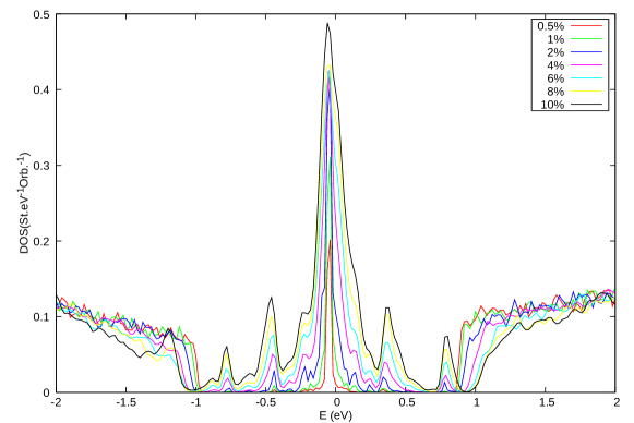
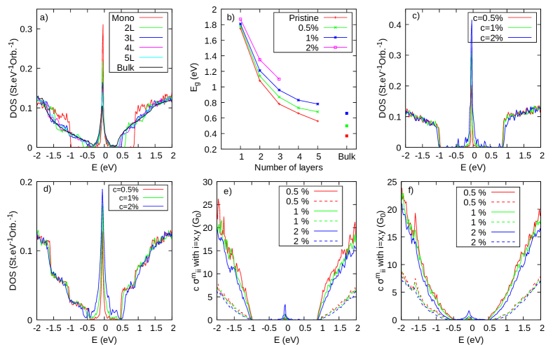
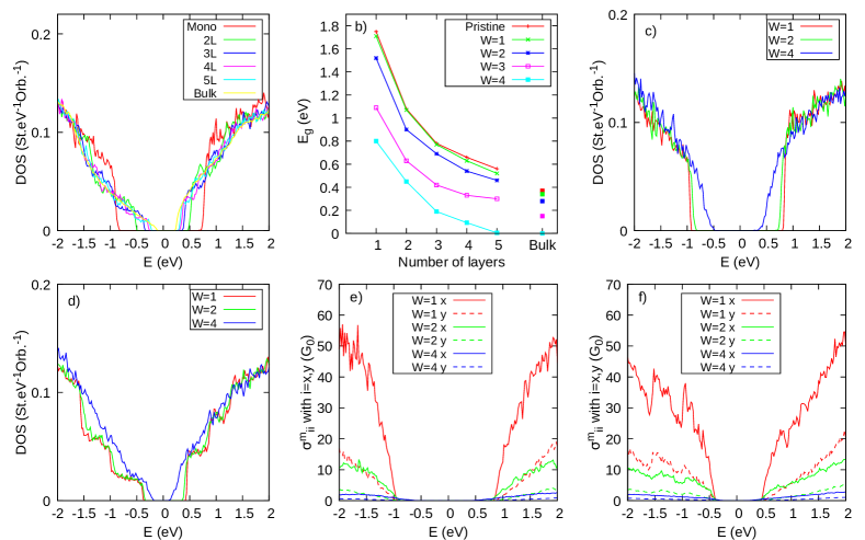
FIG. 3a illustrates the density of states (DOS) for a vacancy concentration of (resonant scatterers) relative to the total number of atoms in monolayer, few-layer BP, and bulk BP. Notably, there is a decrease in the gap as the number of layers increases. The FIG. 3b shows that overall, for few-layer BP (FIG. 3d for 3 layers) and bulk configurations, the gap increases as the vacancy concentration rises, except for the monolayer case where the gap remains nearly constant (FIG. 3c).
We can clearly distinguish the midgap state peak due to vacancies in the gap (FIG. 3a). It is not centered at zero energy because the coupling terms beyond the first neighbors break the electron-hole symmetry of the bipartite Hamiltonian. Its width remains almost constant as the number of layers increases showing that its energy dispersion is mainly due to intralayer couplings between midgap states. As the gap decreases with an increasing number of layers, the specific value of at which the midgap peaks completely fill the gap depends on the number of layers. For monolayer, at studied concentration, the gap is not filled and we can distinguish that secondary peaks appear (see FIGs. S1 in SM [32]). On the other hand, the gap is completely filled for in the case of 5 layers and a bulk, respectively (see FIGs. S2 and S3 in SM [32]). In FIG. 3b, the points corresponding to these particular cases are not represented.
FIGs. 3e,f show the microscopic conductivity multiplied by concentration versus energy for monolayer and trilayer according to the -direction (bold line) –armchair direction– and according to the -direction (dashed line) –zigzag direction–. See also FIG. S4 in SM [32] for bulk BP. The armchair conductivity is greater than the zigzag conductivity for all cases (monolayer, few-layer and bulk). The proportionality between and remains the same for all systems. This ratio is a signature of the structural anisotropy of these materials, which results in an anisotropy of the effective masses of electrons and holes. [34, 69].
Moreover, FIGs. 3e,f show that the conductivity has a behavior according to the Bloch-Boltzmann approach and then the conductivity is proportional to . This result was obtained experimentally when the monolayer of BP is grafted with PtCl2 groups [20]. It is also important to note that midgap states do not contribute much to conduction. Indeed, even if the gap is filled by midgap states there is still a mobility gap. This may not be true for very high defect concentrations, which would allow strong conduction through defect states that would percolate into the structure to form a kind of midgap-state bands.
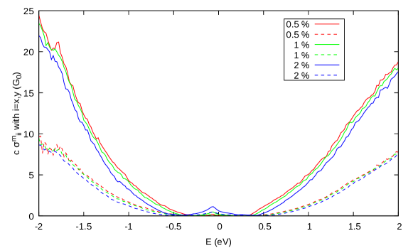
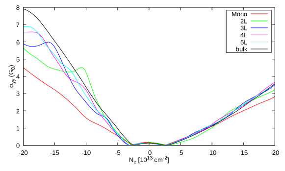
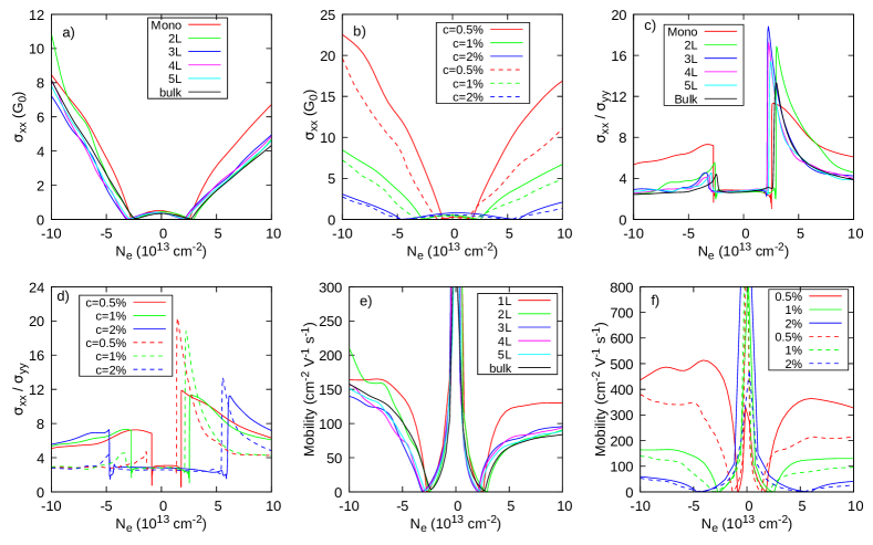
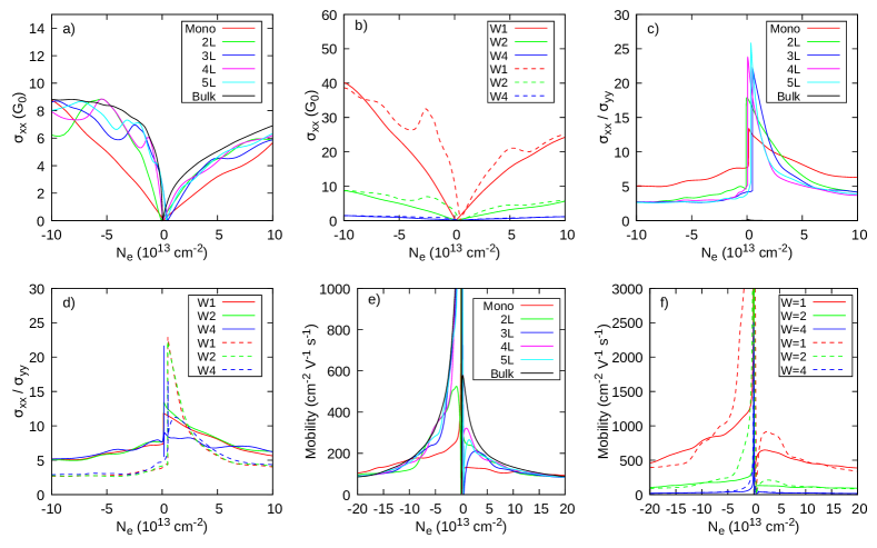
We now study the effect of vacancies on the conductivity and mobility at room temperature ( K) versus the charge carriers (Eqs. (6), (8) and (9)). The prediction of other works are not similar and depends roughly with the numerical study [31]. FIG. 4a shows the armchair conductivity per layer versus for monolayer, few-layer BP, and bulk with a concentration of vacancies of . The conductivity of holes is larger than that of electrons for high values of charge carriers. The zigzag conductivity presents the same behavior (see FIG. S5 in SM Ref. [32]). These results are in agreement with the experimental results found by Xia et al. [7] for a BP thin film.
To compare the effect of the concentration of vacancies, we present the armchair conductivity versus for monolayer (bold line) and trilayer (dashed line) with different concentrations that are shown in FIG. 4b. As expected, the conductivity decreases when increases, moreover we can remark a relative asymmetry concerning the nature of charge carriers (electrons or holes). In FIG. 4c, the ratio is shown for monolayer, few-layer BP and a bulk versus . is more larger than regardless of charge carrier nature. This result is the same than the theoretic predictions [10, 37] and with experimental results [38]. It is easy to see that the anisotropy in the behavior of conductivity is more significant for electrons than for holes for all systems. However, the ratio is larger for monolayer than for the other systems for holes whereas monolayer ratio is smaller for small electron density. This ratio is also independent of a number of vacancies as found previously (Boltzmann transport). This is shown in FIG. 4d for monolayer and trilayer, and this is valid for all systems. Note that the ratio is equal to the mobility ratio .
To enable simpler comparisons with experimental results, we plot the mobility at room temperature versus (FIG. 4e), according to formulas (8) and (9), for monolayer, few layers and the bulk for . In the case of the monolayer, the mobility is of the same order of magnitude regardless of the charge carrier type. However, for other systems, it is slightly lower for electrons compared to holes. This result was obtained experimentally for Ultrathin Black Phosphorus with Cu adatoms [70]. Furthermore, FIG. 4f illustrates that the lower the concentration of vacancies, the more pronounced the difference between the mobility of holes and that of electrons. The presence of a midgap state in the gap changes the value of (because defects here are neutral). It is therefore possible to compare mobility values, but it is more difficult to compare the values of .
IV.2 Non-resonant scatterers
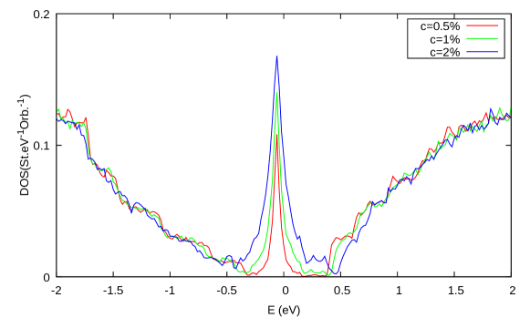
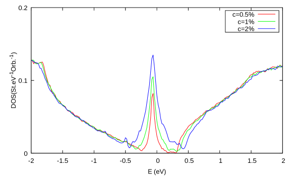
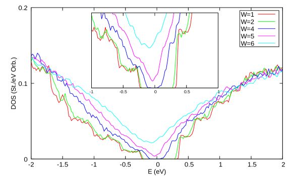
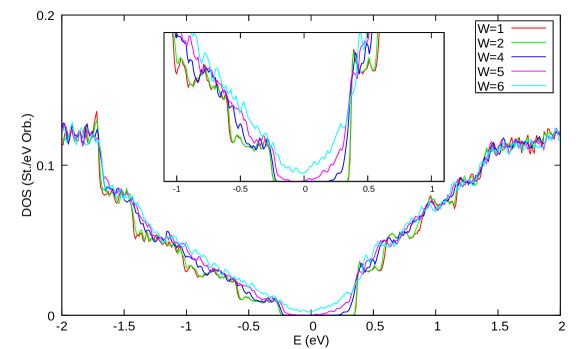
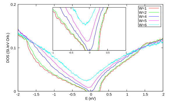
The Anderson disorder (non-resonant scatterers, see Sec. III) is randomly distributed on all layers of the different phosphorus systems studied. FIG. 5a,b and FIGs. S8 in SM [32] show the DOS for monolayer, 2, 3, 4, 5 layers, and bulk BP for different magnitudes of disorder. It is easy to see that the disorder decreases the gap for all systems (FIGs. 5c,d) unlike the case of resonant scatterers. For the bulk and high disorder (), the gap becomes very small ( eV). Most of the recent experiments show the effect of functionalization rather on the surface of BP multilayers to protect it from the deterioration coming from the ambient air. In the case when it is non-covalent, the band gap shrinks down monotonically by increasing the concentration of adsorbates in the topmost layer of few-layer BP.
For large values of , the gap gradually reduces and becomes zero, for bulk and multilayer systems, indicating a semi-conductor/semi-metal transition (see FIGs. S6 and S8 in SM [32]). This result is in good agreement with recent experiments for non-covalent functionalization [71, 72, 25], which validates our hypothesis that the Anderson disorder can model non-covalent adsorbates.
In SM [32], we present the effect of the Anderson disorder only in the top layer of few-layer BP on the band gap (FIG. S7). This shows that the effect of disorder on the gap is qualitatively similar to the case with Anderson disorder randomly distributed across all layers.
FIGs. 5e,f present the armchair microscopic conductivity and zigzag microscopic conductivity , versus energy for monolayer and for 3 layers. As expected due to anisotropy, is always larger than for all values of . It is important to emphasize that the states filling the gap through disorder do not contribute significantly to the conduction. Thus, even though the gap depends quite strongly on the intensity of the disorder, the mobility gap is much less dependent on it.
FIG. 6 presents the effect of Anderson disorder on the conductivity versus charge carriers . The behavior of the conductivity is almost the same for the few-layer BP and the bulk with a slight difference for monolayer, for low values of (FIGs. 6a,b). We can also see that is higher for holes than for electrons. The comparison between and is showed FIGs. 6c,d. Like the case of resonant scatterers (vacancies), the armchair conductivity is larger than the zigzag conductivity and the ratio has the same order as the one obtained in the case of resonant scatterers.
In the FIGs. 6e and f, the mobility at room temperature, calculated according to the formula (8), is shown. As in the case of resonant scatterers, such a calculation can produce numerical artifacts for very small values. Indeed, when (Eq. (9)) tends to zero the conductivity (Eq. (7)) must also tend to zero, which leads to a finite mobility . But because of Gaussian Broadening in calculation of the (Sec. III), is overestimated and may be overestimated for . However, as soon as is not zero, this numerical artifact disappears. Experimentally, it has been shown that for small solvent molecules, which are non-covalent scatterers, and at concentrations on the order of cm-2 and cm-2, the hole mobility is higher than that of electrons [73].
V Discusions and conclusion
Experimentally, phosphorene often contains a large number of local defects that are not always well characterized in the literature. These static defects may be due to the functionalization by adsorbed atoms or molecules, the effect of the substrate, or other structural effects. We aim to study the electronic structure and quantum transport in the presence of a high concentration of these defects. To do this, we considered two extreme types of generic local defects: resonant and non-resonant defects. We used the Rudenko tight binding (TB) model [27, 28] to analyze monolayer Black Phosphorene (BP), few-layer BP, and bulk BP. The TB model used is an effective four-band Hamiltonian, i.e. one effective orbital per P atom which is a -like orbital. This makes it easy to simulate resonant adsorbates by vacancies (vacant P atoms) and non-resonant adsorbates by Anderson disorder (on-site energy disorder).
Concerning the electronic structure, the two types of defect have very different effects on the gap. The resonant scatterers create midgap states that expand when the concentration of defects increases until the gap is filled. Whereas, non-resonant disorder reduces the gap value by filling the gap edges when its magnitude increases, As for resonant disorder, a high concentration of non-resonant disorder can fill the gap. This extreme case is easier to achieve for a multi-layer BP and the bulk BP which have a lower gap.
Quantum diffusion calculations show that resonant and non-resonant defects act similarly on electrical conductivity. Indeed, even for the high defect concentrations we studied, the gap states of resonant defects and the gap edge states of non-resonant defects contribute very little to conductivity, and so the mobility gap remains close to the gap of the defect-free system. This suggests that electronic transport should be fairly well described by a semi-classical Bloch-Boltzamn-type approach, even when defects strongly modify the electronic structure. Particularly, the conductivity of states outside the gap is inversely proportional to the resonant defect concentration . Note that for sufficiently small amounts of defect, when the gap is always present, it is possible to calculate electron mobility, and we obtain values that are entirely comparable to the experimental results.
As expected, the strong anisotropy of BP’s atomic structure induces anisotropy in conductivity and mobility. This anisotropy is stronger in the case of the monolayer BP. And so from 2-layer BP, it is pretty close to that of the bulk BP. Our calculations show that this asymmetry persists in the presence of the two types of defect we have studied. And here again, it is difficult to find very different behavior between resonant defects and non-resonant defects. Comparing our calculations with the conductivity or mobility values found experimentally is difficult, as the defect concentration is not known. However, the anisotropy should be found experimentally. In particular, it would be possible to find experimentally that the ratio versus the charge carrier density exhibits a well-defined peak for small .
Acknowledgments
Numerical calculations have been performed at LPMC, Université de Tunis El Manar, and Centre de Calculs (CDC), CY Cergy Paris Université. We thank warmly Yann Costes and Baptiste Mary, CDC, for computing assistance. GTL and DM was supported by the ANR project J2D (ANR-15-CE24-0017). JJK thanks CY Advanced Studies for financial support.
References
- Cortés-Arriagada et al. [2022] D. Cortés-Arriagada, N. Barria, D. E. Ortega, I. Araya-Durán, and M. Belén Camarada, A first-principles study on the adsorption properties of phosphorene oxide for pollutant removal from water, J. Mol. Liq. 357, 119103 (2022).
- Kumbhakar et al. [2023] P. Kumbhakar, J. S. Jayann, A. Sreedevi Madhavikutty, P. R. Sreeram, A. Saritha, T. Ito, and C. S. Tiwary, Prospective applications of two-dimensional materials beyond laboratory frontiers: A review, iScience 26, 106671 (2023).
- Marian et al. [2022] M. Marian, D. Berman, D. Nečas, N. Emami, A. Ruggiero, and A. Rosenkranz, Roadmap for 2D materials in biotribological/biomedical applications – a review, Adv. Col. Int. Sc. 307, 102747 (2022).
- Long et al. [2019] M. Long, P. Wang, H. Fang, and W. Hu, Progress, challenges, and opportunities for 2D material based photodetectors, Adv. Funct. Mat. 29, 1803807 (2019).
- Li et al. [2014] L. Li, Y. Yu, G. J. Ye, Q. Ge, X. Ou, H. Wu, D. Feng, X. H. Chen, and Y. Zhang, Black phosphorus field-effect transistors, Nature Nanotech. 9, 372 (2014).
- Liu et al. [2014] H. Liu, A. T. Neal, Z. Zhu, Z. Luo, X. Xu, D. Tománek, and P. D. Ye, Phosphorene: An unexplored 2D semiconductor with a high hole mobility, ACS Nano 8, 4033 (2014).
- Xia et al. [2014] F. Xia, H. Wang, and Y. Jia, Rediscovering black phosphorus as an anisotropic layered material for optoelectronics and electronics, Nat. Commun. 5, 4458 (2014).
- Sorkin et al. [2017] V. Sorkin, Y. Cai, Z. Ong, G. Zhang, and Y. W. Zhang, Recent advances in the study of phosphorene and its nanostructures, Critical Reviews in Solid State and Materials Sciences 42, 1 (2017).
- Tran et al. [2014] V. Tran, R. Soklaski, Y. Liang, and L. Yang, Layer-controlled band gap and anisotropic excitons in few-layer black phosphorus, Phys. Rev. B 89, 235319 (2014).
- Qiao et al. [2014] J. Qiao, X. Kong, Z.-X. Hu, F. Yang, and W. Ji, High-mobility transport anisotropy and linear dichroism in few-layer black phosphorus, Nat. Commun. 5, 4475 (2014).
- Denis [2022] P. A. Denis, New insights into the covalent functionalization of black and blue phosphorene, Computational and Theoretical Chemistry 1215, 113839 (2022).
- Mitrović et al. [2021] A. Mitrović, G. Abellán, and A. Hirsch, Covalent and non-covalent chemistry of 2D black phosphorus, RSC Adv. 11, 26093 (2021).
- Ryder et al. [2016] C. R. Ryder, J. D. Wood, S. A. Wells, Y. Yang, D. Jariwala, T. J. Marks, G. C. Schatz, and M. C. Hersam, Covalent functionalization and passivation of exfoliated black phosphorus via aryl diazonium chemistry, Nature Chem. 8, 597 (2016).
- Tang et al. [2017] X. Tang, W. Liang, J. Zhao, Z. Li, M. Qiu, T. Fan, C. S. Luo, Y. Zhou, Y. Li, Z. Guo, D. Fan, and H. Zhang, Fluorinated phosphorene: Electrochemical synthesis, atomistic fluorination, and enhanced stability, Small 13, 1702739 (2017).
- Jellett et al. [2020] C. Jellett, J. Plutnar, and M. Pumera, Prospects for functionalizing elemental 2D pnictogens: A study of molecular models, ACS Nano 14, 7722 (2020).
- van Druenen et al. [2018] M. van Druenen, F. Davitt, T. Collins, C. Glynn, C. O’Dwyer, J. D. Holmes, and G. Collins, Covalent functionalization of few-layer black phosphorus using iodonium salts and comparison to diazonium modified black phosphorus, Chem. Mater. 30, 4667 (2018).
- Yan et al. [2020] S. Yan, H. Song, L. F. Wan, S. Lin, H. Wu, Y. Shi, and J. Yao, Hydroxyl-assisted phosphorene stabilization with robust device performances, Nano Lett. 20, 81 (2020).
- Bui and Yarmohammadi [2018] D. H. Bui and M. Yarmohammadi, Impurity-induced anisotropic semiconductor-semimetal transition in monolayer biased black phosphorus, Phys. Lett. A 382, 1885 (2018).
- Kuklin et al. [2019] A. V. Kuklin, G. V. Baryshnikov, and H. Ågren, Spontaneous decomposition of fluorinated phosphorene and its stable structure, J. Phys. Chem. Lett. 10, 7086 (2019).
- Sun et al. [2019] C. Sun, Y. Wang, Y. Jiang, Z.-D. Yang, G. Zhang, and Y. Hu, Transport and photogalvanic properties of covalent functionalized monolayer black phosphorus, New J. Chem. 43, 377 (2019).
- Liu et al. [2021] Y. Liu, M. Chen, and S. Yang, Chemical functionalization of 2D black phosphorus, InfoMat 3, 231 (2021).
- Antonatos et al. [2022] N. Antonatos, J. Šturala, V. Mazánek, D. Sedmidubský, M. Veselý, K. Růžička, J. Hejtmánek, P. Levinsky, and Z. Sofer, Black phosphorus: Fundamental properties and influence of impurities induced by its synthesis, ACS Appl. Mater. Interfaces 14, 34867 (2022).
- Taylor et al. [2020] P. D. Taylor, S. A. Tawfik, and M. J. S. Spencer, Interplay of mechanical and chemical tunability of phosphorene for flexible nanoelectronic applications, J. Phys. Chem. C 124, 24391 (2020).
- Bolognesi et al. [2019] M. Bolognesi, S. Moschetto, M. Trapani, F. Prescimone, C. Ferroni, G. Manca, A. Ienco, S. Borsacchi, M. Caporali, M. Muccini, M. Peruzzini, M. Serrano-Ruiz, L. Calucci, M. A. Castriciano, and S. Toffanin, Noncovalent functionalization of 2D black phosphorus with fluorescent boronic derivatives of pyrene for probing and modulating the interaction with molecular oxygen, ACS Appl. Mater. Interfaces 11, 22637 (2019).
- Chen et al. [2020] Z. Chen, J. Dong, C. Giorgetti, E. Papalazarou, M. Marsi, Z. Zhang, B. Tian, Q. Ma, Y. Cheng, J.-P. Rueff, A. Taleb-Ibrahimi, and L. Perfetti, Spectroscopy of buried states in black phosphorus with surface doping, 2D Mater. 7, 035027 (2020).
- Wang et al. [2017] C. Wang, D. Niu, B. Liu, S. Wang, X. Wei, Y. Liu, H. Xie, and Y. Gao, Charge transfer at the PTCDA/black phosphorus interface, J. Phys. Chem. C 121, 18084 (2017).
- Rudenko and Katsnelson [2014] A. N. Rudenko and M. I. Katsnelson, Quasiparticle band structure and tight-binding model for single- and bilayer black phosphorus, Phys. Rev. B 89, 201408 (2014).
- Rudenko et al. [2015] A. N. Rudenko, S. Yuan, and M. I. Katsnelson, Toward a realistic description of multilayer black phosphorus: From approximation to large-scale tight-binding simulations, Phys. Rev. B 92, 085419 (2015).
- Goulart et al. [2019] L. Goulart, L. da S. Fernandes, C. Lange dos Santos, and J. Rossato, Electronic and structural properties of black phosphorene doped with Si, B and N, Phys. Lett. A 383, 125945 (2019).
- Ding and Wang [2015] Y. Ding and Y. Wang, Structural, electronic, and magnetic properties of adatom adsorptions on black and blue phosphorene: A first-principles study, J. Phys. Chem. C 119, 10610 (2015).
- Yuan et al. [2015] S. Yuan, A. N. Rudenko, and M. I. Katsnelson, Transport and optical properties of single- and bilayer black phosphorus with defects, Phys. Rev. B 91, 115436 (2015).
- [32] See Supplemental Material at http://xxxx for figures to complement the figures in the main text.
- Takao et al. [1981] Y. Takao, H. Asahina, and A. Morita, Electronic structure of black phosphorus in tight binding approach, J. Phys. Soc. Jpn. 50, 3362 (1981).
- Carvalho et al. [2016] A. Carvalho, M. Wang, X. Zhu, A. S. Rodin, H. Su, and A. H. Castro Neto, Phosphorene: from theory to applications, Nat. Rev. Mater. 1, 16061 (2016).
- Batmunkh et al. [2016] M. Batmunkh, M. Bat-Erdene, and J. G. Shapter, Phosphorene and phosphorene-based materials – prospects for future applications, Adv. Mater. 28, 8586 (2016).
- He et al. [2015] J. He, D. He, Y. Wang, Q. Cui, M. Z. Bellus, H.-Y. Chiu, and H. Zhao, Exceptional and anisotropic transport properties of photocarriers in black phosphorus, ACS nano 9, 6436 (2015).
- Liu et al. [2016] Y. Liu, T. Low, and P. P. Ruden, Mobility anisotropy in monolayer black phosphorus due to scattering by charged impurities, Phys. Rev. B 93, 165402 (2016).
- Haratipour et al. [2018] N. Haratipour, Y. Liu, R. J. Wu, S. Namgung, P. P. Ruden, K. A. Mkhoyan, S.-H. Oh, and S. J. Koester, Mobility anisotropy in black phosphorus MOSFETs with HfO2 gate dielectrics, IEEE Transactions on Electron Devices 65, 4093 (2018).
- Skachkova [2018] V. Skachkova, Electronic properties of phosphorene with vacancies: ab initio study, Materials Physics and Mechanics 39, 35 (2018).
- Li et al. [2015] X.-B. Li, P. Guo, T.-F. Cao, H. Liu, W.-M. Lau, and L.-M. Liu, Structures, stabilities and electronic properties of defects in monolayer black phosphorus, Sci. Rep. 5, 10848 (2015).
- Motohiko [2014] E. Motohiko, Topological origin of quasi-flat edge band in phosphorene, New J. Phys. 16, 115004 (2014).
- Taghizadeh Sisakht et al. [2015] E. Taghizadeh Sisakht, M. H. Zare, and F. Fazileh, Scaling laws of band gaps of phosphorene nanoribbons: A tight-binding calculation, Phys. Rev. B 91, 085409 (2015).
- Vahedi and Peters [2021] J. Vahedi and R. Peters, Edge magnetic properties of black phosphorene nanoribbons, Phys. Rev. B 103, 075108 (2021).
- Kapildeb and Su Ying [2015] D. Kapildeb and Q. Su Ying, Quantum-confinement and structural anisotropy result in electrically-tunable dirac cone in few-layer black phosphorous, Sci. Rep. 5, 11699 (2015).
- Pereira and Katsnelson [2015] J. M. Pereira and M. I. Katsnelson, Landau levels of single-layer and bilayer phosphorene, Phys. Rev. B 92, 075437 (2015).
- Wu et al. [2020] J.-Y. Wu, W.-P. Su, and G. Gumbs, Anomalous magneto-transport properties of bilayer phosphorene, Sci. Rep. 10, 7674 (2020).
- Abdelsalam et al. [2018] H. Abdelsalam, V. A. Saroka, I. Lukyanchuk, and M. E. Portnoi, Multilayer phosphorene quantum dots in an electric field: Energy levels and optical absorption, J. Appl. Phys. 124, 124303 (2018).
- Ma et al. [2021] R. Ma, H. T. Cao, and L. Wang, Anomalous magneto-thermoelectric transport in biased bilayer phosphorene, Eur. Phys. J. B 94, 93 (2021).
- Peng et al. [2014] X. Peng, Q. Wei, and A. Copple, Strain-engineered direct-indirect band gap transition and its mechanism in two-dimensional phosphorene, Phys. Rev. B 90, 085402 (2014).
- Castellanos-Gomez et al. [2014] A. Castellanos-Gomez, L. Vicarelli, E. Prada, J. O. Island, K. L. Narasimha-Acharya, S. I. Blanter, D. J. Groenendijk, M. Buscema, G. A. Steele, J. V. Alvarez, and et al., Isolation and characterization of few-layer black phosphorus, 2D Mater. 1, 025001 (2014).
- Wang et al. [2015] X. Wang, A. M. Jones, K. L. Seyler, V. Tran, Y. Jia, H. Zhao, H. Wang, L. Yang, X. Xu, and F. Xia, Highly anisotropic and robust excitons in monolayer black phosphorus, Nature Nanotech. 10, 517 (2015).
- Mayou [1988] D. Mayou, Calculation of the conductivity in the short-mean-free-path regime, EPL 6, 549 (1988).
- Mayou and Khanna [1995] D. Mayou and S. K. Khanna, A real-space approach to electronic transport, J. Phys. I France 5, 1199 (1995).
- Roche and Mayou [1997] S. Roche and D. Mayou, Conductivity of quasiperiodic systems: A numerical study, Phys. Rev. Lett. 79, 2518 (1997).
- Roche and Mayou [1999] S. Roche and D. Mayou, Formalism for the computation of the RKKY interaction in aperiodic systems, Phys. Rev. B 60, 322 (1999).
- Triozon et al. [2002] F. Triozon, J. Vidal, R. Mosseri, and D. Mayou, Quantum dynamics in two- and three-dimensional quasiperiodic tilings, Phys. Rev. B 65, 220202 (2002).
- Missaoui et al. [2017] A. Missaoui, J. J. Khabthani, N.-E. Jaidane, D. Mayou, and G. Trambly de Laissardière, Numerical analysis of electronic conductivity in graphene with resonant adsorbates: comparison of monolayer and Bernal bilayer, Eur. Phys. J. B 90, 75 (2017).
- Missaoui et al. [2018] A. Missaoui, J. J. Khabthani, N.-E. Jaidane, D. Mayou, and G. Trambly de Laissardière, Mobility gap and quantum transport in a functionalized graphene bilayer, J. Phys.: Condens. Matter 30, 195701 (2018).
- Trambly de Laissardière and Mayou [2013] G. Trambly de Laissardière and D. Mayou, Conductivity of graphene with resonant and nonresonant adsorbates, Phys. Rev. Lett. 111, 146601 (2013).
- Lherbier et al. [2012] A. Lherbier, S. M.-M. Dubois, X. Declerck, Y.-M. Niquet, S. Roche, and J.-C. Charlier, Transport properties of graphene containing structural defects, Phys. Rev. B 86, 075402 (2012).
- Roche et al. [2012] S. Roche, N. Leconte, F. Ortmann, A. Lherbier, D. Soriano, and J.-C. Charlier, Quantum transport in disordered graphene: A theoretical perspective, Sol. State Comm. 152, 1404 (2012).
- Cresti et al. [2013] A. Cresti, F. Ortmann, T. Louvet, D. Van Tuan, and S. Roche, Broken symmetries, zero-energy modes, and quantum transport in disordered graphene: From supermetallic to insulating regimes, Phys. Rev. Lett. 110, 196601 (2013).
- Namarvar et al. [2020] O. F. Namarvar, A. Missaoui, L. Magaud, D. Mayou, and G. Trambly de Laissardière, Electronic structure and quantum transport in twisted bilayer graphene with resonant scatterers, Phys. Rev. B 101, 245407 (2020).
- Latil et al. [2004] S. Latil, S. Roche, D. Mayou, and J.-C. Charlier, Mesoscopic transport in chemically doped carbon nanotubes, Phys. Rev. Lett. 92, 256805 (2004).
- Ishii et al. [2010] H. Ishii, S. Roche, N. Kobayashi, and K. Hirose, Inelastic transport in vibrating disordered carbon nanotubes: Scattering times and temperature-dependent decoherence effects, Phys. Rev. Lett. 104, 116801 (2010).
- Jemaï et al. [2019] G. Jemaï, J. J. Khabthani, G. Trambly de Laissardière, and D. Mayou, Quantum localization and electronic transport in covalently functionalized carbon nanotubes, J. Phys.: Condens. Matter 32, 115301 (2019).
- Lacroix et al. [2020] A. Lacroix, G. T. de Laissardière, P. Quémerais, J.-P. Julien, and D. Mayou, Modeling of electronic mobilities in halide perovskites: Adiabatic quantum localization scenario, Phys. Rev. Lett. 124, 196601 (2020).
- Khabthani et al. [2021] J. J. Khabthani, A. Missaoui, D. Mayou, and G. Trambly de Laissardière, Electronic transport properties and quantum localization effects monitored by selective functionalization in Bernal bilayer graphene, Phys. Rev. B 104, 245125 (2021).
- Akhtar et al. [2017] M. Akhtar, G. Anderson, R. Zhao, A. Alruqi, J. E. Mroczkowska, G. Sumanasekera, and J. B. Jasinski, Recent advances in synthesis, properties, and applications of phosphorene, npj 2D Mater Appl 1, 5 (2017).
- Koenig et al. [2016] S. P. Koenig, R. A. Doganov, L. Seixas, A. Carvalho, J. Y. Tan, K. Watanabe, T. Taniguchi, N. Yakovlev, A. H. Castro Neto, and B. Özyilmaz, Electron doping of ultrathin black phosphorus with Cu adatoms, Nano Lett. 16, 2145 (2016).
- Kim et al. [2015] J. Kim, S. S. Baik, S. H. Ryu, Y. Sohn, S. Park, B.-G. Park, J. Denlinger, Y. Yi, H. J. Choi, and K. S. Kim, Observation of tunable band gap and anisotropic Dirac semimetal state in black phosphorus, Science 349, 723 (2015).
- Kim et al. [2017] S.-W. Kim, H. Jung, H.-J. Kim, J.-H. Choi, S.-H. Wei, and J.-H. Cho, Microscopic mechanism of the tunable band gap in potassium-doped few-layer black phosphorus, Phys. Rev. B 96, 075416 (2017).
- Wang et al. [2019] Y. Wang, A. Slassi, J. Cornil, D. Beljonne, and P. Samorì, Tuning the optical and electrical properties of few-layer black phosphorus via physisorption of small solvent molecules, Small 15, 1903432 (2019).
*
Appendix A
Supplemental Material
for
Electronic structure and conductivity in multilayer Black Phosphorene with resonant and non-resonant scatterers
Jouda Jemaa Khabthani, Khouloud Chika, Ghassen Jemaï, Didier Mayou, Guy Trambly de Laissardière
In this Supplementary Information, additional figures are shown to support arguments given in the main text.