Understanding Trap States in InP and GaP Quantum Dots Through Density Functional Theory
Abstract
The widespread application of III-V colloidal quantum dots (QDs) as non-toxic, highly tunable emitters is stymied by their high density of trap states. Here, we utilize density functional theory (DFT) to investigate trap state formation in a diverse set of realistically passivated core-only InP and GaP QDs. Through orbital localization techniques, we deconvolute the dense manifold of trap states to allow for detailed assignment of surface defects. We find that the three-coordinate species dominate trapping in III-V QDs and identify features in the geometry and charge environment of trap centers capable of deepening, or sometimes passivating, traps. Furthermore, we observe stark differences in surface reconstruction between InP and GaP, where the more labile InP reconstructs to passivate three-coordinate indium at the cost of distortion elsewhere. These results offer explanations for experimentally observed trapping behavior and suggest new avenues for controlling trap states in III-V QDs.
keywords:
quantum dots, indium phosphide, gallium phosphide, cadmium-free, density functional theory, trap state![[Uncaptioned image]](/html/2403.00703/assets/x1.png)
For Table of Contents Only
1
Colloidal semiconductor nanocrystals, more commonly known as quantum dots (QDs), have attracted considerable attention as solution-processable materials 1, 2 with highly tunable optical properties 3, 4, 5, 6, 7, 8. They have begun to see use in a wide range of applications including photovoltaics 9, 10, photodetectors 2, 11, LEDs 1, 12, lasing 13, 14, drug delivery 15, 16, biological imaging 17, 18, and quantum computing 19, 20. However, the QDs with the best performance to date 21, 22, 23 are those composed of highly toxic and internationally-restricted cadmium or lead chalcogenides 24, 25, 26, making the development of a non-toxic alternative material with equally strong optical properties necessary for safe widespread commercialization. III-V QDs, namely indium phosphide (InP), are promising candidates for this replacement due to their low toxicity 25, 26 and widely tunable emission range 18, 27. Until recently, their implementation has been held back by generally low quantum yields and broad emission line widths relative to their II-VI counterparts 28, 29, 30, 31, 32. These phenomena are often understood to result from a high density of trap states: occupied or virtual electronic states, usually localized on the surface of the QD, with energies between the valence band maximum (VBM) and conduction band minimum (CBM) 31, 33. While recent advances in control over III-V core/shell heterostructures have led to InP QDs with near-unity quantum yields 12, 34, 35, a complete atomistic understanding of the formation and character of surface traps in III-V QDs remains elusive, especially for core-only QDs.
Trap states are not unique to III-V QDs; a vast body of both experimental and theoretical literature discusses trap states in II-VI QDs 33, 36, 37, 38, 39, 40, 41, 42, 43, 44, 45, IV-VI QDs 33, 46, 47, 48, and lead halide perovskite nanocrystals 33, 49, 50, 51. The most widely accepted origin of trap states is under-coordinated surface atoms 31, 38, 50, 51, 52, 53, 54, 55, 56, 57, 42, although in certain systems excess charge 37, 39, imperfect stoichiometry 46, and substitutional defects 58 have also been implicated. For CdSe, several studies employing density functional theory (DFT) have shown that trap states arise primarily from two-coordinate Se atoms (Se-2c) but not Se-3c or any under-coordinated Cd 38, 40, 41. No such consensus has been reached for InP QDs, however. Many studies have implied that hole trapping dominates in InP QDs 36, 53, 56, 57, 58, 59, 60, 61, but there is also considerable evidence for the presence of electron traps, especially in the absence of a core/shell heterostructure 31, 52, 54, 55. This disagreement has been compounded by a relative lack of atomistic ab initio studies of trap states in InP QDs 52, 54, 55, 56, 57, 58, 62, 63, 64, many of which only employ less-accurate GGA functionals. Studies have variously emphasized P-3c traps 57, In-3c traps 55, 64, both In-3c and P-3c traps but with disagreement on their respective depths 52, 54, traps from the two-coordinate species with additional P-3c traps only in tetrahedral geometries 56, as well as studies that find InP QDs with both In-3c and P-3c to be trap free but see traps introduced upon different surface treatments 58, 63. Most of these studies only compute the electronic structure of a single model InP QD, limiting generalizability with respect to shape, size, faceting, and surface passivation. Moreover, very few studies have applied computation to understand trap states in other III-V QDs such as gallium phosphide (GaP) 65, a promising but under-studied emissive material 66, 67.
Here, we use DFT to study a large and diverse set of InP and GaP QDs and draw generalized conclusions on the nature of their trap states and the factors that influence trap depth. The six base QD morphologies studied here are summarized in Figure 1. Several important decisions inform the development of our test set. We focus on core-only QDs, carved from the corresponding bulk crystal using a well-established construction procedure 40, 68. In this way we create six starting QDs for both InP and GaP, chosen to represent distinct faceting and shape. The four larger models, with a diameter of 2.3 nm for the quasispherical QDs and an edge length of 3.0 nm for the tetrahedral QDs, represent the upper limit of computationally realizable QDs. The two smaller models allow for size extrapolation. Surfaces are passivated with F- ligands, representative of the well-established treatment of InP QDs with HF 31, 55, as a way of balancing computational efficiency with realistic passivation. Calculations show that larger halogen ligands create states close to the VBM, potentially interfering with the assignment of trap and bulk states (SI, Section I.I).
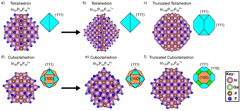
The construction procedure employed for these starting QDs is analagous to the ones used in previous ab initio studies of trap states in III-V QDs (SI, Section I.II), and results in some number of three-coordinate In/Ga and P atoms in all starting structures 55, 56, 57, 58, 63. The difficulty in creating perfectly four-coordinate III-V model QD surfaces arises from charge-orbital balance, in which the formal charge of each atom in a QD must add to the total charge of the system to prevent doping 69. While some experimental evidence exists suggesting QDs must be strictly charge-neutral 70, 71, it has also been shown that strict charge-balance greatly limits the shapes of possible III-V QDs, and additionally restricts the possible defects one could induce to these QDs to charge neutrality 56. To extend the range of QD shapes and defects available to us without inducing doping, we allow for slight positive charges in our structures 37, 72. The restriction to positive charges serves not only to avoid exacerbating DFT’s self-interaction error 73, but also allows our cation-rich systems to have their charge balanced by the fluoride counter-ions available in solution 53. We find this to be an effective solution, observing no doping in any of our systems and no qualitative difference in geometry or electronic structure between our charged and neutral models.
We diversify our dataset and study the effects of surface reconstruction by creating a variety of "defective" QDs out of the starting models discussed above. These defective structures are created in a similar manner to previous studies, but our lack of charge neutrality affords us a greater variety of available defects 52, 38, 33, 72, 56, 54, 50, 41. In short, when creating defects in a starting structure we consider all the symmetry-unique removals of a single \chF-, \chP^3-, \chInF_x unit, and \chInP unit, as described in more detail the Supporting Information, Section I.III. This procedure results in a total library of 98 InP and GaP QDs for consideration.
We then compute the ground state electronic structure of each QD using the hybrid functional PBE0, as hybrid functionals are known to be necessary for the accurate reproduction of band gaps 74, 75. Comprehensive identification of trap states requires the prior identification of the first delocalized bulk state, i.e. the VBM and CBM. This is made challenging by the dense manifold of intermediately localized states near the band edges, as summarized in Figure 2. Two techniques are used to visualize the band structure of our models. The first is the projected density of states (PDOS), which can be used to visualize contributions from different atomic species and different coordination numbers to each band as a function of energy (Figure 2a,c). The second is the participation ratio (PR), which measures the localization of each electronic state (Figure 2b,d), defined in the Supporting Information, Section II.II.
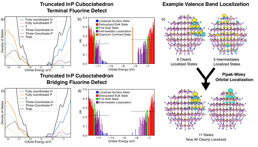
A naive analysis of the Kohn-Sham eigenstates is problematic because localization is not an intrinsic property of the DFT Kohn-Sham eigenstate 76, 77. In fact, any linear combination of degenerate eigenfunctions is also a solution to the Kohn-Sham equations, and in many systems the these linear combinations will be more delocalized relative than what experiment and chemical intuition would suggest, especially when the eigenstate spectrum is particularly dense 78. Confronted with this problem, we can utilize orbital localization methods, such as Foster-Boys 79 and Pipek-Mizey 80, to perform unitary transformations on a selected subset of molecular orbitals to maximize their localization. In fact, applying Pipek-Mizey localization to the band edges of our QDs reveals that many states with intermediate delocalization reduce to linear combinations of a dense set of clearly localized trap states, as exampled in Figure 2e. Combined with the observation that “true” bulk states fail to localize into clear surface states, orbital localization gives us a powerful tool to test for the location of the VBM and CBM. Our procedure is described in detail in the Supporting Information, Section II.III. For example, the VBM is chosen to be the highest energy delocalized occupied state without a disproportionate contribution from under-coordinated P, and all occupied states above it in energy should be localizable into clearly surface-bound trap states. All such higher energy states are then taken to be hole trap states, with trap depth equal to the difference between their energy and the energy of the VBM. An analagous definition identifies the CBM and associated electron traps.
An additional complication in this analysis arises when considering the conduction band due to the intermittent presence of the highly-delocalized quantum-confined S-like state 3, 81, 82. While not a trap state, the quantum-confined state cannot be considered the true CBM either, as it is not present in all structures. This is evidenced in Figures 2b and 2d, where both structures have identical stoichiometry, shape, faceting, and charge but the former displays the quantum-confined state and the latter does not. The majority of our QDs do not display this quantum-confined state and we have found no chemical justification for why some structures do while others do not. Nevertheless, the algorithm above produces consistent VBM, CBM, and trap depths if we simply exclude the quantum confined state from consideration - i.e. when present, the quantum confined state is neither a trap nor the CBM. We observe no general qualitative difference between the trap states in QDs with and without the quantum-confined state.
The defective QD structures reveal an immediate difference in surface reconstruction between InP and GaP, exemplified in Figures 3a and 3b. While GaP is relatively rigid with little reconstruction after defect induction, InP reconstructs heavily both in the immediate vicinity of the defect and further afield. Representative of all QDs studied here, we use the smaller tetrahedral QD in Figure 3 as a particularly clear example of this effect. Degree of reconstruction can be quantitatively measured though reorganization energies, which we find to be over three times larger on average in InP than in GaP (SI, Section III.I). We hypothesize the origin of this contrast to be In’s greater affinity for anionic ligands than Ga, due to its lower electronegativity. However, we note that the observed trends in reconstruction still hold when Cl ligands are employed instead of F (SI, Section III.II). These results are supported by prior experimental findings for InGaP, where Ga is found to reside disproportionately at the surface, and In to Ga substitution is found to be thermodynamically favorable, increasing QD stability and narrowing X-ray peaks 83, 84.
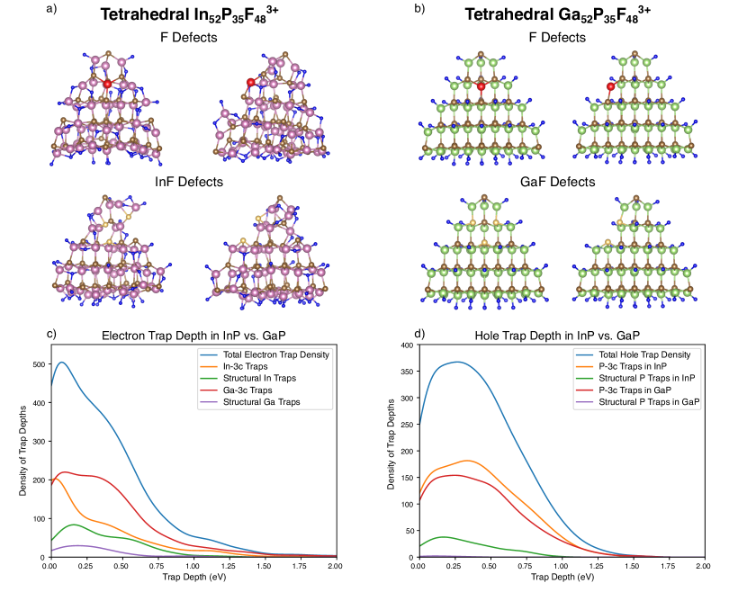
The greater reconstruction in InP leads to differences in the depth distribution of electron and hole traps between the two materials, shown in Figures 3c and 3d. Across our data set there are fewer In-3c in InP than there are Ga-3c in GaP, and slightly more P-3c in InP than in GaP (SI, Section III.I). The cost of the passivation of In-3c is evidenced in the extensive formation of additional electron trap states localized around distorted In-4c atoms, here denoted “structural” traps. While localized with mid-gap energies, these structural traps appear to arise not from under-coordinated surface species but rather from structural deformations caused by extensive surface reconstruction. We do not delve deeply into the nature and origin of these structural traps here; for now, we simply note their presence, even before orbital localization is applied. Despite these additional structural traps, electron traps in InP are generally less deep than those in GaP, with many In-3c being non-trapping or very shallowly trapping. This finding agrees with experimental results for InGaP nanowires, where nonradiative recombination increases with increasing Ga concentration 85. P-based hole traps, on the other hand, have a similar distribution of depths across InP and GaP QDs (Figure 3d).
Close analysis of electron traps in InP and GaP QDs reveals two distinct geometries of the three-coordinate cation, which lead to distinct distributions of trap depths (Figures 4a and 4b). We designate these geometries as planar, when the cation is coplanar with its coordinated atoms, and pyramidal, when the cation is out of said plane. While both geometries are present in both InP and GaP, they occur with different proportions. Planar Ga-3c is dominant over pyramidal Ga-3c, while planar and pyramidal In-3c have similar prevalence. This further explains the aforementioned surface reconstruction in InP, where planar In-3c is more likely to convert to the pyramidal geometry in order for ligands to bridge to additional In-3c. In both materials, however, traps arising from the pyramidal geometry are significantly deeper, on average, than those from the planar geometry. In InP this difference is such that most planar In-3c are effectively non-trapping. In fact, the reconstruction of In-3c from planar to pyramidal partially counteracts an innate overall increased depth of Ga-3c traps over In-3c traps. By separating the two geometries, we see that on average traps from planar Ga-3c (0.29 eV) are deeper than those from planar In-3c (0.19 eV), and that traps from pyramidal Ga-3c (0.66 eV) are deeper than those from pyramidal In-3c (0.45 eV).
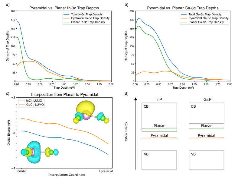
To understand the origin of these differing trap depths, we performed interpolations between the pyramidal and planar geometries of both \chInCl3 and \chGaCl3 (Figure 4c). We find that the differences between pyramidal and planar defects can be understood using simple molecular arguments. As we interpolate from planar to pyramidal (SI, Section IV.I), we observe that the LUMO, which corresponds to the trap state, decreases in energy by around 0.7 eV in both InP and GaP. This is accompanied by a shift of electron density onto the metal in the LUMO, as can be seen in the orbital plots in Figure 4c and through ChELPG charge analysis (SI, Section IV.II) 86. This shift of charge makes the LUMO more lone-pair-like, lowering the energy of the anti-bonding state into the band gap, resulting in a deeper trap. However, this analysis does not explain the difference between the electron trap depths in InP and GaP. These differences most likely arise from GaP’s wider band gap 56, 84, as summarized in Figure 4d, where trap states that are shallow in GaP can become non-trapping as the CBM decreases in energy. We find support for this idea through additional interpolations between four-coordinate and three-coordinate \chInCl4 and \chGaCl4 (SI, Section IV.III).
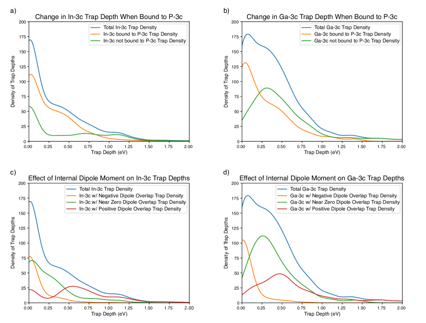
Even when accounting for the differing depths of pyramidal and planar traps, the distributions of electron trap depths in Figures 4a and 4b remain quite broad. These shifts can be explained primarily through two electrostatic effects intrinsic to the trap centers’ local environment. First, we observe that In-3c and Ga-3c bound to P-3c have shallower traps on average than those without, as shown in Figures 5a and 5b, respectively. This can be understood by recognizing P-3c as having an excess of negative charge, which destabilizes the nearby trap state and raises its energy near (or above) the CBM. A similar effect exists in reverse for hole traps, where P-3c bound to In-3c have shallower traps as the excess positive charge of the In-3c stabilizes the trap state and lowers its energy (SI, Section V). The second effect arises from the internal dipole moment of the QD. In both real QDs and our models, any asymmetry will lead to the creation of an internal dipole moment which can shift the depth of trap states, as has been previously noted for perovskite NCs 51. We show this effect for In-3c and Ga-3c in Figures 5c and 5d, computing the dipole overlap as the dot product between the dipole moment (pointing toward the positive charge) and the position vector of the trap center. We observe that a positive dipole overlap deepens trap states, whereas a negative dipole overlap almost always makes In-3c and Ga-3c nontrapping. Again, a similar effect exists in reverse for P-3c (SI, Section V). As expected from their covalency difference, this effect is stronger for InP than GaP. By removing both electrostatic effects we achieve even better agreement with our interpolations, finding average trap depths of 0.12 eV for planar In-3c, 0.37 eV for planar Ga-3c, 0.69 eV for pyramidal In-3c, and 0.92 eV for pyramidal Ga-3c.
Note that we have not included traps from two-coordinate atoms in the above discussion. Such species appear in our dataset, and moreover cause deep traps when they appear (SI, Section VI). However, we find that surface reconstruction in both InP and GaP is sufficient to passivate the majority of two-coordinate defects when created, and we do not observe indirect creation of any two-coordinate species. We thus conclude that two-coordinate species are at best minor contributors to trapping in real InP and GaP QDs.
In conclusion, we have investigated the prevalence, character, and depth of trap states in InP and GaP QDs using DFT. Our results are kept generalizable through the study of 98 QDs with variable size, shape, and surface defects. Through orbital localization, we deconvolute the dense band edge to identify otherwise evasive trap states including as yet unexplored “structural” traps tied to distorted fully-coordinated atoms. We leverage our dataset to analyze trends in trap depth arising from cation species, cation geometry, and local electrostatic effects which provide avenues for trap control. These results yield important insights into trap states in InP and GaP QDs, as well as informing guidelines for effective simulation of trap states in general QDs. Future directions include detailed investigation of the origin and character of the structural traps observed here, as well as the study of trap states in other III-V materials such as InGaP and III-V core-shell heterostructures. Investigation into the effects of chemical doping on trap state formation, as well as the efficacy of different surface passivation schemes, is necessary to gain a complete picture of trap states in III-V QDs. Finally, it would be instructive to investigate the excited state electronic structure of III-V QDs directly using, for example, time-dependent DFT.
This work was supported by the German Research Foundation (DFG, KI 2558/1-1). We would like to thank the MIT School of Science, MIT Chemistry Department, and the Office of Graduate Education for support of this work through the Dean of Science Fellowship.
The Supporting Information is available free of charge at XXX
-
•
Ligand choice, construction procedure, defect induction procedure, computational details, participation ratio, procedure for identification of 1st bulk state, reconstruction energies, reconstruction with Cl ligands, interpolation details, ChELPG charge analysis, interpolation from four-coordinate to three-coordinate, broadening of hole trap depths, two-coordinate traps (PDF)
References
- Dai et al. 2014 Dai, X.; Zhang, Z.; Jin, Y.; Niu, Y.; Cao, H.; Liang, X.; Chen, L.; Wang, J.; Peng, X. Solution-processed, high-performance light-emitting diodes based on quantum dots. Nature 2014, 515, 96–99
- García de Arquer et al. 2017 García de Arquer, F. P.; Armin, A.; Meredith, P.; Sargent, E. H. Solution-processed semiconductors for next-generation photodetectors. Nature Reviews Materials 2017, 2, 1–17
- Bawendi et al. 1990 Bawendi, M. G.; Steigerwald, M. L.; Brus, L. E. The Quantum Mechanics of Larger Semiconductor Clusters ("Quantum Dots"). Annual Review of Physical Chemistry 1990, 41, 477–496
- Murray et al. 1993 Murray, C. B.; Norris, D. J.; Bawendi, M. G. Synthesis and characterization of nearly monodisperse CdE (E = sulfur, selenium, tellurium) semiconductor nanocrystallites. Journal of the American Chemical Society 1993, 115, 8706–8715
- Alivisatos 1996 Alivisatos, A. P. Semiconductor Clusters, Nanocrystals, and Quantum Dots. Science 1996, 271, 933–937
- Talapin et al. 2010 Talapin, D. V.; Lee, J.-S.; Kovalenko, M. V.; Shevchenko, E. V. Prospects of Colloidal Nanocrystals for Electronic and Optoelectronic Applications. Chemical Reviews 2010, 110, 389–458
- Boles et al. 2016 Boles, M. A.; Ling, D.; Hyeon, T.; Talapin, D. V. The surface science of nanocrystals. Nature Materials 2016, 15, 141–153
- Kagan et al. 2016 Kagan, C. R.; Lifshitz, E.; Sargent, E. H.; Talapin, D. V. Building devices from colloidal quantum dots. Science 2016, 353, aac5523
- Semonin et al. 2011 Semonin, O. E.; Luther, J. M.; Choi, S.; Chen, H.-Y.; Gao, J.; Nozik, A. J.; Beard, M. C. Peak External Photocurrent Quantum Efficiency Exceeding 100% via MEG in a Quantum Dot Solar Cell. Science 2011, 334, 1530–1533
- Scalise 2019 Scalise, E. Tailoring the electronic properties of semiconducting nanocrystal-solids. Semiconductor Science and Technology 2019, 35, 013001
- Livache et al. 2019 Livache, C.; Martinez, B.; Goubet, N.; Gréboval, C.; Qu, J.; Chu, A.; Royer, S.; Ithurria, S.; Silly, M. G.; Dubertret, B.; Lhuillier, E. A colloidal quantum dot infrared photodetector and its use for intraband detection. Nature Communications 2019, 10, 2125
- Won et al. 2019 Won, Y.-H.; Cho, O.; Kim, T.; Chung, D.-Y.; Kim, T.; Chung, H.; Jang, H.; Lee, J.; Kim, D.; Jang, E. Highly efficient and stable InP/ZnSe/ZnS quantum dot light-emitting diodes. Nature 2019, 575, 634–638
- Fan et al. 2017 Fan, F. et al. Continuous-wave lasing in colloidal quantum dot solids enabled by facet-selective epitaxy. Nature 2017, 544, 75–79
- Park et al. 2021 Park, Y.-S.; Roh, J.; Diroll, B. T.; Schaller, R. D.; Klimov, V. I. Colloidal quantum dot lasers. Nature Reviews Materials 2021, 6, 382–401
- Mura et al. 2013 Mura, S.; Nicolas, J.; Couvreur, P. Stimuli-responsive nanocarriers for drug delivery. Nature Materials 2013, 12, 991–1003
- Patra et al. 2018 Patra, J. K.; Das, G.; Fraceto, L. F.; Campos, E. V. R.; Rodriguez-Torres, M. d. P.; Acosta-Torres, L. S.; Diaz-Torres, L. A.; Grillo, R.; Swamy, M. K.; Sharma, S.; Habtemariam, S.; Shin, H.-S. Nano based drug delivery systems: recent developments and future prospects. Journal of Nanobiotechnology 2018, 16, 1–33
- Medintz et al. 2005 Medintz, I. L.; Uyeda, H. T.; Goldman, E. R.; Mattoussi, H. Quantum dot bioconjugates for imaging, labelling and sensing. Nature Materials 2005, 4, 435–446
- Saeboe et al. 2021 Saeboe, A. M.; Nikiforov, A. Y.; Toufanian, R.; Kays, J. C.; Chern, M.; Casas, J. P.; Han, K.; Piryatinski, A.; Jones, D.; Dennis, A. M. Extending the Near-Infrared Emission Range of Indium Phosphide Quantum Dots for Multiplexed In Vivo Imaging. Nano Letters 2021, 21, 3271–3279
- Ladd et al. 2010 Ladd, T. D.; Jelezko, F.; Laflamme, R.; Nakamura, Y.; Monroe, C.; O’Brien, J. L. Quantum computers. Nature 2010, 464, 45–53
- Zajac et al. 2018 Zajac, D. M.; Sigillito, A. J.; Russ, M.; Borjans, F.; Taylor, J. M.; Burkard, G.; Petta, J. R. Resonantly driven CNOT gate for electron spins. Science 2018, 359, 439–442
- Dai et al. 2017 Dai, X.; Deng, Y.; Peng, X.; Jin, Y. Quantum-Dot Light-Emitting Diodes for Large-Area Displays: Towards the Dawn of Commercialization. Advanced Materials 2017, 29, 1607022
- Hanifi et al. 2019 Hanifi, D. A.; Bronstein, N. D.; Koscher, B. A.; Nett, Z.; Swabeck, J. K.; Takano, K.; Schwartzberg, A. M.; Maserati, L.; Vandewal, K.; van de Burgt, Y.; Salleo, A.; Alivisatos, A. P. Redefining near-unity luminescence in quantum dots with photothermal threshold quantum yield. Science 2019, 363, 1199–1202
- García de Arquer et al. 2021 García de Arquer, F. P.; Talapin, D. V.; Klimov, V. I.; Arakawa, Y.; Bayer, M.; Sargent, E. H. Semiconductor quantum dots: Technological progress and future challenges. Science 2021, 373, eaaz8541
- Derfus et al. 2004 Derfus, A. M.; Chan, W. C. W.; Bhatia, S. N. Probing the Cytotoxicity of Semiconductor Quantum Dots. Nano Letters 2004, 4, 11–18
- Reiss et al. 2016 Reiss, P.; Carrière, M.; Lincheneau, C.; Vaure, L.; Tamang, S. Synthesis of Semiconductor Nanocrystals, Focusing on Nontoxic and Earth-Abundant Materials. Chemical Reviews 2016, 116, 10731–10819
- Allocca et al. 2019 Allocca, M.; Mattera, L.; Bauduin, A.; Miedziak, B.; Moros, M.; De Trizio, L.; Tino, A.; Reiss, P.; Ambrosone, A.; Tortiglione, C. An Integrated Multilevel Analysis Profiling Biosafety and Toxicity Induced by Indium- and Cadmium-Based Quantum Dots in Vivo. Environmental Science & Technology 2019, 53, 3938–3947
- Reiss et al. 2009 Reiss, P.; Protière, M.; Li, L. Core/Shell Semiconductor Nanocrystals. Small 2009, 5, 154–168
- Cros-Gagneux et al. 2010 Cros-Gagneux, A.; Delpech, F.; Nayral, C.; Cornejo, A.; Coppel, Y.; Chaudret, B. Surface Chemistry of InP Quantum Dots: A Comprehensive Study. Journal of the American Chemical Society 2010, 132, 18147–18157
- Cui et al. 2013 Cui, J.; Beyler, A. P.; Marshall, L. F.; Chen, O.; Harris, D. K.; Wanger, D. D.; Brokmann, X.; Bawendi, M. G. Direct probe of spectral inhomogeneity reveals synthetic tunability of single-nanocrystal spectral linewidths. Nature Chemistry 2013, 5, 602–606
- Tamang et al. 2016 Tamang, S.; Lincheneau, C.; Hermans, Y.; Jeong, S.; Reiss, P. Chemistry of InP Nanocrystal Syntheses. Chemistry of Materials 2016, 28, 2491–2506
- Hughes et al. 2019 Hughes, K. E.; Stein, J. L.; Friedfeld, M. R.; Cossairt, B. M.; Gamelin, D. R. Effects of Surface Chemistry on the Photophysics of Colloidal InP Nanocrystals. ACS Nano 2019, 13, 14198–14207
- Jang et al. 2020 Jang, E.; Kim, Y.; Won, Y.-H.; Jang, H.; Choi, S.-M. Environmentally Friendly InP-Based Quantum Dots for Efficient Wide Color Gamut Displays. ACS Energy Letters 2020, 5, 1316–1327
- Giansante and Infante 2017 Giansante, C.; Infante, I. Surface Traps in Colloidal Quantum Dots: A Combined Experimental and Theoretical Perspective. The Journal of Physical Chemistry Letters 2017, 8, 5209–5215
- Van Avermaet et al. 2022 Van Avermaet, H.; Schiettecatte, P.; Hinz, S.; Giordano, L.; Ferrari, F.; Nayral, C.; Delpech, F.; Maultzsch, J.; Lange, H.; Hens, Z. Full-Spectrum InP-Based Quantum Dots with Near-Unity Photoluminescence Quantum Efficiency. ACS Nano 2022, 16, 9701–9712
- Li et al. 2022 Li, H.; Zhang, W.; Bian, Y.; Ahn, T. K.; Shen, H.; Ji, B. ZnF2-Assisted Synthesis of Highly Luminescent InP/ZnSe/ZnS Quantum Dots for Efficient and Stable Electroluminescence. Nano Letters 2022, 22, 4067–4073
- Kirkwood et al. 2018 Kirkwood, N.; Monchen, J. O. V.; Crisp, R. W.; Grimaldi, G.; Bergstein, H. A. C.; du Fossé, I.; van der Stam, W.; Infante, I.; Houtepen, A. J. Finding and Fixing Traps in II–VI and III–V Colloidal Quantum Dots: The Importance of Z-Type Ligand Passivation. Journal of the American Chemical Society 2018, 140, 15712–15723
- Voznyy et al. 2013 Voznyy, O.; Thon, S. M.; Ip, A. H.; Sargent, E. H. Dynamic Trap Formation and Elimination in Colloidal Quantum Dots. The Journal of Physical Chemistry Letters 2013, 4, 987–992, Publisher: American Chemical Society
- Houtepen et al. 2017 Houtepen, A. J.; Hens, Z.; Owen, J. S.; Infante, I. On the Origin of Surface Traps in Colloidal II–VI Semiconductor Nanocrystals. Chemistry of Materials 2017, 29, 752–761
- du Fossé et al. 2019 du Fossé, I.; ten Brinck, S.; Infante, I.; Houtepen, A. J. Role of Surface Reduction in the Formation of Traps in n-Doped II–VI Semiconductor Nanocrystals: How to Charge without Reducing the Surface. Chemistry of Materials 2019, 31, 4575–4583
- Goldzak et al. 2021 Goldzak, T.; McIsaac, A. R.; Van Voorhis, T. Colloidal CdSe nanocrystals are inherently defective. Nature Communications 2021, 12, 890
- McIsaac et al. 2023 McIsaac, A. R.; Goldzak, T.; Van Voorhis, T. It Is a Trap!: The Effect of Self-Healing of Surface Defects on the Excited States of CdSe Nanocrystals. The Journal of Physical Chemistry Letters 2023, 14, 1174–1181, Publisher: American Chemical Society
- Kilina et al. 2009 Kilina, S.; Ivanov, S.; Tretiak, S. Effect of Surface Ligands on Optical and Electronic Spectra of Semiconductor Nanoclusters. Journal of the American Chemical Society 2009, 131, 7717–7726
- Wei et al. 2012 Wei, H. H.-Y.; Evans, C. M.; Swartz, B. D.; Neukirch, A. J.; Young, J.; Prezhdo, O. V.; Krauss, T. D. Colloidal Semiconductor Quantum Dots with Tunable Surface Composition. Nano Letters 2012, 12, 4465–4471
- Elward and Chakraborty 2013 Elward, J. M.; Chakraborty, A. Effect of Dot Size on Exciton Binding Energy and Electron–Hole Recombination Probability in CdSe Quantum Dots. Journal of Chemical Theory and Computation 2013, 9, 4351–4359
- Califano et al. 2005 Califano, M.; Franceschetti, A.; Zunger, A. Temperature Dependence of Excitonic Radiative Decay in CdSe Quantum Dots: The Role of Surface Hole Traps. Nano Letters 2005, 5, 2360–2364
- Kim et al. 2013 Kim, D.; Kim, D.-H.; Lee, J.-H.; Grossman, J. C. Impact of Stoichiometry on the Electronic Structure of PbS Quantum Dots. Physical Review Letters 2013, 110, 196802
- Chuang et al. 2015 Chuang, C.-H. M.; Maurano, A.; Brandt, R. E.; Hwang, G. W.; Jean, J.; Buonassisi, T.; Bulović, V.; Bawendi, M. G. Open-Circuit Voltage Deficit, Radiative Sub-Bandgap States, and Prospects in Quantum Dot Solar Cells. Nano Letters 2015, 15, 3286–3294
- Vörös et al. 2017 Vörös, M.; Brawand, N. P.; Galli, G. Hydrogen Treatment as a Detergent of Electronic Trap States in Lead Chalcogenide Nanoparticles. Chemistry of Materials 2017, 29, 2485–2493
- Shao et al. 2014 Shao, Y.; Xiao, Z.; Bi, C.; Yuan, Y.; Huang, J. Origin and elimination of photocurrent hysteresis by fullerene passivation in CH3NH3PbI3 planar heterojunction solar cells. Nature Communications 2014, 5, 5784
- Nenon et al. 2018 Nenon, D. P.; Pressler, K.; Kang, J.; Koscher, B. A.; Olshansky, J. H.; Osowiecki, W. T.; Koc, M. A.; Wang, L.-W.; Alivisatos, A. P. Design Principles for Trap-Free CsPbX3 Nanocrystals: Enumerating and Eliminating Surface Halide Vacancies with Softer Lewis Bases. Journal of the American Chemical Society 2018, 140, 17760–17772
- Du Fossé et al. 2022 Du Fossé, I.; Mulder, J. T.; Almeida, G.; Spruit, A. G. M.; Infante, I.; Grozema, F. C.; Houtepen, A. J. Limits of Defect Tolerance in Perovskite Nanocrystals: Effect of Local Electrostatic Potential on Trap States. Journal of the American Chemical Society 2022, 144, 11059–11063
- Fu and Zunger 1997 Fu, H.; Zunger, A. InP quantum dots: Electronic structure, surface effects, and the redshifted emission. Physical Review B 1997, 56, 1496–1508
- Stein et al. 2016 Stein, J. L.; Mader, E. A.; Cossairt, B. M. Luminescent InP Quantum Dots with Tunable Emission by Post-Synthetic Modification with Lewis Acids. The Journal of Physical Chemistry Letters 2016, 7, 1315–1320
- Cho et al. 2018 Cho, E.; Kim, T.; Choi, S.-m.; Jang, H.; Min, K.; Jang, E. Optical Characteristics of the Surface Defects in InP Colloidal Quantum Dots for Highly Efficient Light-Emitting Applications. ACS Applied Nano Materials 2018, 1, 7106–7114
- Kim et al. 2018 Kim, T.-G.; Zherebetskyy, D.; Bekenstein, Y.; Oh, M. H.; Wang, L.-W.; Jang, E.; Alivisatos, A. P. Trap Passivation in Indium-Based Quantum Dots through Surface Fluorination: Mechanism and Applications. ACS Nano 2018, 12, 11529–11540
- Dümbgen et al. 2021 Dümbgen, K. C.; Zito, J.; Infante, I.; Hens, Z. Shape, Electronic Structure, and Trap States in Indium Phosphide Quantum Dots. Chemistry of Materials 2021, 33, 6885–6896
- Dümbgen et al. 2023 Dümbgen, K. C.; Leemans, J.; De Roo, V.; Minjauw, M.; Detavernier, C.; Hens, Z. Surface Chemistry of InP Quantum Dots, Amine–Halide Co-Passivation, and Binding of Z-Type Ligands. Chemistry of Materials 2023, 35, 1037–1046
- Janke et al. 2018 Janke, E. M.; Williams, N. E.; She, C.; Zherebetskyy, D.; Hudson, M. H.; Wang, L.; Gosztola, D. J.; Schaller, R. D.; Lee, B.; Sun, C.; Engel, G. S.; Talapin, D. V. Origin of Broad Emission Spectra in InP Quantum Dots: Contributions from Structural and Electronic Disorder. Journal of the American Chemical Society 2018, 140, 15791–15803
- Calvin et al. 2020 Calvin, J. J.; Swabeck, J. K.; Sedlak, A. B.; Kim, Y.; Jang, E.; Alivisatos, A. P. Thermodynamic Investigation of Increased Luminescence in Indium Phosphide Quantum Dots by Treatment with Metal Halide Salts. Journal of the American Chemical Society 2020, 142, 18897–18906
- Richter et al. 2019 Richter, A. F.; Binder, M.; Bohn, B. J.; Grumbach, N.; Neyshtadt, S.; Urban, A. S.; Feldmann, J. Fast Electron and Slow Hole Relaxation in InP-Based Colloidal Quantum Dots. ACS Nano 2019, 13, 14408–14415
- Enright et al. 2022 Enright, M. J. et al. Role of Atomic Structure on Exciton Dynamics and Photoluminescence in NIR Emissive InAs/InP/ZnSe Quantum Dots. The Journal of Physical Chemistry C 2022, 126, 7576–7587
- Park et al. 2021 Park, N.; Eagle, F. W.; DeLarme, A. J.; Monahan, M.; LoCurto, T.; Beck, R.; Li, X.; Cossairt, B. M. Tuning the interfacial stoichiometry of InP core and InP/ZnSe core/shell quantum dots. The Journal of Chemical Physics 2021, 155, 084701
- Ubbink et al. 2022 Ubbink, R. F.; Almeida, G.; Iziyi, H.; du Fossé, I.; Verkleij, R.; Ganapathy, S.; van Eck, E. R. H.; Houtepen, A. J. A Water-Free In Situ HF Treatment for Ultrabright InP Quantum Dots. Chemistry of Materials 2022, 34, 10093–10103
- Hassan et al. 2018 Hassan, A.; Zhang, X.; Liu, C.; Snee, P. T. Electronic Structure and Dynamics of Copper-Doped Indium Phosphide Nanocrystals Studied with Time-Resolved X-ray Absorption and Large-Scale DFT Calculations. The Journal of Physical Chemistry C 2018, 122, 11145–11151
- Zhu et al. 2023 Zhu, D.; Bahmani Jalali, H.; Saleh, G.; Di Stasio, F.; Prato, M.; Polykarpou, N.; Othonos, A.; Christodoulou, S.; Ivanov, Y. P.; Divitini, G.; Infante, I.; De Trizio, L.; Manna, L. Boosting the Photoluminescence Efficiency of InAs Nanocrystals Synthesized with Aminoarsine via a ZnSe Thick-Shell Overgrowth. Advanced Materials 2023, 35, 2303621
- Kim et al. 2014 Kim, S.; Lee, K.; Kim, S.; Kwon, O.-P.; Heo, J. H.; Im, S. H.; Jeong, S.; Lee, D. C.; Kim, S.-W. Origin of photoluminescence from colloidal gallium phosphide nanocrystals synthesized via a hot-injection method. RSC Advances 2014, 5, 2466–2469
- Choi et al. 2023 Choi, Y.; Choi, C.; Bae, J.; Park, J.; Shin, K. Synthesis of gallium phosphide quantum dots with high photoluminescence quantum yield and their application as color converters for LEDs. Journal of Industrial and Engineering Chemistry 2023, 123, 509–516
- Geva et al. 2018 Geva, N.; Shepherd, J. J.; Nienhaus, L.; Bawendi, M. G.; Van Voorhis, T. Morphology of Passivating Organic Ligands around a Nanocrystal. The Journal of Physical Chemistry C 2018, 122, 26267–26274
- Voznyy et al. 2012 Voznyy, O.; Zhitomirsky, D.; Stadler, P.; Ning, Z.; Hoogland, S.; Sargent, E. H. A Charge-Orbital Balance Picture of Doping in Colloidal Quantum Dot Solids. ACS Nano 2012, 6, 8448–8455
- Fritzinger et al. 2010 Fritzinger, B.; Capek, R. K.; Lambert, K.; Martins, J. C.; Hens, Z. Utilizing Self-Exchange To Address the Binding of Carboxylic Acid Ligands to CdSe Quantum Dots. Journal of the American Chemical Society 2010, 132, 10195–10201
- Moreels et al. 2011 Moreels, I.; Justo, Y.; De Geyter, B.; Haustraete, K.; Martins, J. C.; Hens, Z. Size-Tunable, Bright, and Stable PbS Quantum Dots: A Surface Chemistry Study. ACS Nano 2011, 5, 2004–2012
- Zherebetskyy et al. 2015 Zherebetskyy, D.; Zhang, Y.; Salmeron, M.; Wang, L.-W. Tolerance of Intrinsic Defects in PbS Quantum Dots. The Journal of Physical Chemistry Letters 2015, 6, 4711–4716
- Vydrov et al. 2007 Vydrov, O. A.; Scuseria, G. E.; Perdew, J. P. Tests of functionals for systems with fractional electron number. The Journal of Chemical Physics 2007, 126, 154109
- Kurth et al. 1999 Kurth, S.; Perdew, J. P.; Blaha, P. Molecular and solid-state tests of density functional approximations: LSD, GGAs, and meta-GGAs. International Journal of Quantum Chemistry 1999, 75, 889–909
- Azpiroz et al. 2014 Azpiroz, J. M.; Ugalde, J. M.; Infante, I. Benchmark Assessment of Density Functional Methods on Group II–VI MX (M = Zn, Cd; X = S, Se, Te) Quantum Dots. Journal of Chemical Theory and Computation 2014, 10, 76–89
- Boys 1960 Boys, S. F. Construction of Some Molecular Orbitals to Be Approximately Invariant for Changes from One Molecule to Another. Reviews of Modern Physics 1960, 32, 296–299, Publisher: American Physical Society
- Lehtola and Jónsson 2013 Lehtola, S.; Jónsson, H. Unitary Optimization of Localized Molecular Orbitals. Journal of Chemical Theory and Computation 2013, 9, 5365–5372
- Truhlar 2012 Truhlar, D. G. Are Molecular Orbitals Delocalized? Journal of Chemical Education 2012, 89, 573–574
- Foster and Boys 1960 Foster, J. M.; Boys, S. F. Canonical Configurational Interaction Procedure. Reviews of Modern Physics 1960, 32, 300–302, Publisher: American Physical Society
- Pipek and Mezey 1989 Pipek, J.; Mezey, P. G. A fast intrinsic localization procedure applicable for ab initio and semiempirical linear combination of atomic orbital wave functions. The Journal of Chemical Physics 1989, 90, 4916–4926
- Ellingson et al. 2003 Ellingson, R. J.; Blackburn, J. L.; Nedeljkovic, J.; Rumbles, G.; Jones, M.; Fu, H.; Nozik, A. J. Theoretical and experimental investigation of electronic structure and relaxation of colloidal nanocrystalline indium phosphide quantum dots. Physical Review B 2003, 67, 075308
- Shulenberger et al. 2021 Shulenberger, K. E.; Coppieters ‘t Wallant, S. C.; Klein, M. D.; McIsaac, A. R.; Goldzak, T.; Berkinsky, D. B.; Utzat, H.; Barotov, U.; Van Voorhis, T.; Bawendi, M. G. Resolving the Triexciton Recombination Pathway in CdSe/CdS Nanocrystals through State-Specific Correlation Measurements. Nano Letters 2021, 21, 7457–7464
- Lebedev et al. 2016 Lebedev, M. V.; Kalyuzhnyy, N. A.; Mintairov, S. A.; Calvet, W.; Kaiser, B.; Jaegermann, W. Comparison of wet chemical treatment and Ar-ion sputtering for GaInP2(100) surface preparation. Materials Science in Semiconductor Processing 2016, 51, 81–88
- Hudson et al. 2022 Hudson, M. H.; Gupta, A.; Srivastava, V.; Janke, E. M.; Talapin, D. V. Synthesis of In1–xGaxP Quantum Dots in Lewis Basic Molten Salts: The Effects of Surface Chemistry, Reaction Conditions, and Molten Salt Composition. The Journal of Physical Chemistry C 2022, 126, 1564–1580
- Zhang et al. 2017 Zhang, W.; Zeng, X.; Su, X.; Zou, X.; Mante, P.-A.; Borgström, M. T.; Yartsev, A. Carrier Recombination Processes in Gallium Indium Phosphide Nanowires. Nano Letters 2017, 17, 4248–4254
- Breneman and Wiberg 1990 Breneman, C. M.; Wiberg, K. B. Determining atom-centered monopoles from molecular electrostatic potentials. The need for high sampling density in formamide conformational analysis. Journal of Computational Chemistry 1990, 11, 361–373, _eprint: https://onlinelibrary.wiley.com/doi/pdf/10.1002/jcc.540110311